


 |
市場調查報告書
商品編碼
2044018
半導體晶圓回收:市場佔有率分析、產業趨勢與統計、成長預測(2026-2031)Semiconductor Wafer Reclaim - Market Share Analysis, Industry Trends & Statistics, Growth Forecasts (2026 - 2031) |
||||||
※ 本網頁內容可能與最新版本有所差異。詳細情況請與我們聯繫。
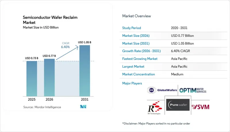
2025 年半導體晶圓回收市場價值為 7.3 億美元,預計到 2031 年將達到 10.5 億美元,而 2026 年為 7.7 億美元,預測期(2026-2031 年)複合年成長率為 6.4%。
先進製程日益成長的資本密集度,以及循環製造的監管要求,正推動半導體製造商轉向使用回收晶圓。這種轉變降低了測試和監控晶圓的總擁有成本,減少了碳排放,並在新晶圓價格波動的情況下降低了供應鏈風險。此外,人工智慧驅動的檢測技術已將處理時間從數天縮短至數小時,使回收晶圓供應商能夠跟上晶圓廠大規模生產的步伐。同時,亞太地區密集叢集的300毫米晶圓廠構成了需求基礎,而新興的碳化矽(SiC)和氮化鎵(GaN)中試生產線正在為化合物半導體回收晶圓市場開闢新的商機。由於實現95%以上良率所需的化學機械拋光(CMP)和測量基礎設施構成了一定的進入門檻,因此市場競爭仍然較為溫和。
全球半導體晶圓回收市場趨勢及洞察
擴大亞太地區300毫米晶圓廠產能
在亞太地區,預計2027年,大部分新增的300毫米晶圓生產線將投入使用,這將推高翻新測試晶圓的基準需求,使其佔各晶圓廠每月開工量的15%至20%。新加坡和台灣的新工廠每月將新增超過200萬片晶圓開工量,每片晶圓可透過翻新重複使用5至7次,進而提高半導體晶圓翻新市場的數量彈性。此外,該地區的高度集中已將物流週期縮短至48小時以內,使翻新供應能夠與準時制生產計劃相匹配。因此,供應商正在大型晶圓廠附近設立工廠,並簽訂多年合約以穩定現金流。隨著產能的進一步擴張,翻新將成為晶圓廠規劃的結構性要素,而不僅僅是戰術性的成本削減措施。
最佳化測試和監控晶圓成本的壓力
目前,全新測試晶圓的成本為每片300mm 120-150美元,預計從2024年起將上漲18%,這將對邏輯、記憶體和功率晶片晶圓廠的毛利率造成壓力。翻新後的基板經過5-8次使用後,其有效成本可降至25-35美元,從而即時節省成本。領先的代工廠已證明,翻新後的監測晶圓在不影響良率的情況下,能夠滿足測量精度要求。裝置製造商也採用機器學習模型來預測剩餘的翻新週期,確保只有當表面粗糙度接近臨界閾值值時才丟棄晶圓。雖然在成熟節點上經濟效益最為顯著,但目前即使在5nm製程工廠中,晶圓的翻新也被用於裝置製造以外的其他工藝,例如腔室老化。
2nm節點嚴格的表面缺陷規範
對於2nm節點的環柵(GaA)電晶體,表面缺陷密度要求低於每平方公分0.1個缺陷,即使在翻新過程中經過多次拋光循環,也很難保證達到這一水準。原子級清洗需要額外增加每片晶圓15-20美元的成本,抵消了任何成本節約,因此先進節點晶圓廠將翻新晶圓的使用限制在非關鍵製程。在供應商能夠可靠地證明其平整度低於0.1nm之前,翻新晶圓在尖端邏輯生產線中的應用將受到限制,從而限制半導體晶圓翻新市場中最有價值的細分領域的成長潛力。
細分市場分析
到2025年,300毫米規格的晶圓將佔總銷售量的52.84%,支撐著邏輯和記憶體晶圓廠半導體晶圓回收市場的規模。然而,預計200毫米規格的晶圓市場在2026年至2031年間將以7.28%的年均成長率成長,成長速度超過其他所有規格。汽車和工業領域的公司繼續青睞成熟的製程節點,例如電源管理積體電路和微機電系統(MEMS)等應用,這些應用能夠有效地適應200毫米設備。一條新的碳化矽試生產線將進一步擴大目標市場。回收供應商透過在傳統拋光機上加裝終點檢測感測器,無需大量資本投入即可提高利潤率,從而在保持設備完全折舊免稅額的情況下實現亞奈米級精度控制。隨著電氣化進程的加速,儘管300毫米生產線仍將保持絕對主導,但200毫米回收生產線的產量將縮小與300毫米生產線的銷售差距。
在航太和抗輻射加固電路等細分領域,對 150 毫米晶圓回收的需求依然存在,這主要得益於衛星星系對小直徑晶圓的青睞,因為小直徑晶圓能夠降低專用晶片的成本效益。化合物半導體基板通常先以 150 毫米為基準進行推廣,然後再逐步擴大尺寸,這為供應商提供了未來滿足寬能隙需求的先機。整體而言,這種直徑配置凸顯了半導體晶圓回收市場的發展趨勢,不僅遵循莫耳定律,最終用戶的經濟效益也將隨之變化。供應商若能將業務拓展至 150 毫米至 300 毫米的生產線,便可降低對特定技術週期的依賴,並隨著每個直徑規格的重要性日益凸顯而獲得增量成長。
區域分析
預計到2025年,亞太地區將佔全球收入的63.79%,並在2031年之前維持6.92%的年均成長率。這項成長主要由台灣、韓國、中國大陸和新加坡推動,這四個地區擁有全球整體300毫米晶圓總產能的三分之二以上。晶圓集中化策略已將晶圓運輸時間縮短至兩天以內,降低了晶圓廠的在製品庫存,並將回收確立為標準營運流程。中國的「雙循環」政策進一步加速了國內回收能力的提升,並將本地供應商打造為抵禦地緣政治衝擊和出口限制的緩衝力量。
預計到2025年,北美將佔全球銷售額的約18%,而《晶片再加工和加工法案》(CHIPS Act)的補貼正在推動從亞利桑那州到德克薩斯州的眾多新晶圓廠的建設。這些新工廠從一開始就整合了再加工車間,體現了資金籌措指南中納入的循環經濟設計原則。儘管技術純熟勞工短缺仍然是一個障礙,但社區大學的認證課程正在逐步彌補這一缺口,這表明中期內區域產能將進一步擴張,美國半導體晶圓再加工市場的需求也將更加穩固。
預計到2025年,歐洲將佔全球銷售額的約12%,歐盟《晶片法案》強制要求分配回收矽以支持供應商的訂單訂單。義大利和奧地利的一家合資企業將原生矽和回收矽整合到同一工廠中,從而減少物流排放並滿足監管要求。世界其他地區佔據剩餘佔有率,其中以色列成熟的微電子產業叢集以及中東地區新的晶圓廠建設計畫預計從2028年起產生額外的需求。因此,區域趨勢與晶圓廠投資而非終端市場消費相關,成長集中在那些資本正流入新建晶圓廠的地區。
其他好處:
- Excel格式的市場預測(ME)表
- 3個月的分析師支持
目錄
第1章:引言
- 研究假設和市場定義
- 調查範圍
第2章:調查方法
第3章執行摘要
第4章 市場狀況
- 市場概覽
- 市場促進因素
- 擴大亞太地區300毫米晶圓廠產能
- 最佳化測試和監控晶圓成本的壓力
- 支持循環經濟實踐的永續發展法規
- 利用人工智慧驅動的產量影像分析工具提高收集產量。
- 對低地球軌道衛星次市場的需求
- 由於代工廠轉向SiC/GaN試製晶圓,需要進行恢復
- 市場限制因素
- 2nm節點嚴格的表面缺陷規範
- 先進拋光生產線熟練工人短缺
- 廢矽價格波動不明朗
- 製造到物流的網路安全風險
- 宏觀經濟因素對市場的影響
- 產業價值鏈分析
- 監理情勢
- 技術展望
- 波特五力分析
- 新進入者的威脅
- 供應商的議價能力
- 買方的議價能力
- 替代品的威脅
- 競爭公司之間的競爭
第5章 市場規模與成長預測
- 依晶圓直徑
- 150 mm
- 200 mm
- 300 mm
- 依晶片類型
- 回收晶圓以進行測試和監測
- 優質晶圓回收
- 外延晶片的回收
- SOI晶圓回收
- 按設備製造類別
- 儲存裝置
- 邏輯裝置
- 類比功率元件
- 專用裝置(MEMS、感測器、射頻)
- 研發設施
- 按地區
- 北美洲
- 歐洲
- 亞太地區
- 世界其他地區
第6章 競爭情勢
- 市場集中度
- 策略趨勢
- 市佔率分析
- 公司簡介
- RS Technologies Co., Ltd.
- Pure Wafer, Inc.
- GlobalWafers Co., Ltd.
- Optim Wafer Services Ltd.
- Silicon Valley Microelectronics, Inc.
- Phoenix Silicon International Corp.
- NanoSILICON, Inc.
- ReSilicon Group LLC
- Kay M Analytics Pte Ltd.
- Siltronic AG
- SUMCO Corporation
- Wafer World, Inc.
- Noel Technologies, Inc.
- PSEMI Corporation
- SiWave Technologies GmbH
- MicroTech Systems, Inc.
- WaferNET, Inc.
- Silicon Materials, Inc.
- REC Silicon ASA
- SilRec SpA
第7章 市場機會與未來展望
The semiconductor wafer reclaim market size was valued at USD 0.73 billion in 2025 and estimated to grow from USD 0.77 billion in 2026 to reach USD 1.05 billion by 2031, at a CAGR of 6.4% during the forecast period (2026-2031).
Heightened capital intensity at advanced nodes, paired with regulatory requirements for circular manufacturing, is steering integrated device manufacturers toward reclaimed substrates. The shift lowers total cost of ownership for test and monitor wafers, trims carbon footprints, and buffers supply-chain risk as virgin-wafer pricing stays volatile. Artificial-intelligence-driven inspection now compresses turnaround from days to hours, letting reclaim vendors match the cadence of high-volume fabs. Meanwhile, Asia-Pacific's dense 300 mm fab cluster anchors demand, while emerging silicon-carbide and gallium-nitride pilot lines open white-space opportunities in compound-semiconductor reclaim. Competitive intensity remains moderate because the chemical-mechanical polishing and metrology infrastructure required for yields above 95% creates natural entry barriers.
Global Semiconductor Wafer Reclaim Market Trends and Insights
Expanding 300 mm Fab Capacity In Asia-Pacific
Asia-Pacific is set to add the bulk of new 300 mm lines through 2027, lifting baseline demand for reclaimed test wafers that account for 15%-20% of every fab's monthly starts. New plants in Singapore and Taiwan add more than 2 million wafer starts per month, each of which can be reused five to seven times when reclaimed, driving volume elasticity for the semiconductor wafer reclaim market. Dense regional clustering also trims logistics to sub-48-hour cycles, aligning reclaim supply with just-in-time production schedules. Vendors are therefore co-locating facilities near megafabs, locking in multiyear contracts that stabilize cash flow. As additional capacity ramps, reclaim ceases to be a tactical cost lever and becomes a structural component of fab planning.
Cost-Optimization Pressure On Test And Monitor Wafers
Virgin test wafers now cost USD 120-USD 150 per 300 mm piece, up 18% since 2024, pinching gross margins for logic, memory, and power fabs. Reclaimed substrates drop the effective cost to USD 25-USD 35 after five to eight cycles, yielding immediate savings. Large foundries have validated that reclaimed monitor wafers meet metrology precision without yield loss. Device makers are also deploying machine-learning models to predict remaining reclaim cycles, ensuring wafers retire only when surface roughness limits approach critical thresholds. The economic case is strongest at mature nodes, but even 5 nm facilities now reclaim wafers for non-device steps such as chamber seasoning.
Stringent Surface-Defect Specs For 2 nm Node
Gate-all-around transistors at 2 nm demand surface-defect densities below 0.1 defects per cm2, a level reclaim processes struggle to guarantee after multiple polish cycles. The need for atomic-layer cleansing steps adds USD 15-USD 20 per wafer, eroding savings and confining reclaimed wafers to non-critical steps in advanced-node fabs. Until vendors demonstrate repeatable sub-0.1 nm flatness, leading-edge logic lines will cap reclaim penetration, limiting upside in the most valuable segment of the semiconductor wafer reclaim market.
Other drivers and restraints analyzed in the detailed report include:
- Sustainability Regulations Favoring Circular-Economy Practices
- AI-Enabled Yield-Imaging Tools Boosting Reclaim Yields
- Limited Skilled Labor For Advanced Polishing Lines
For complete list of drivers and restraints, kindly check the Table Of Contents.
Segment Analysis
The 300 mm format accounted for 52.84% of 2025 revenue, anchoring the semiconductor wafer reclaim market size for logic and memory fabs. Yet the 200 mm segment is forecast to rise at 7.28% during 2026-2031, outpacing all other diameters. Automotive and industrial players continue to favor mature nodes for power-management ICs and micro-electromechanical systems, applications that map efficiently onto 200 mm tooling. New silicon-carbide pilot lines at this diameter further widen the addressable base. Reclaim vendors retrofit legacy polishers with endpoint-detection sensors, delivering sub-nanometer control while preserving fully depreciated equipment, which lifts margins without heavy capital outlays. As electrification accelerates, 200 mm reclaim volume will narrow the revenue gap with 300 mm lines even though the latter retains absolute leadership.
Demand for 150 mm reclaim persists in niche aerospace and radiation-hardened circuits, aided by satellite constellations that prefer smaller diameters for cost control on specialized die. Compound-semiconductor substrates often debut at 150 mm before scaling, giving vendors an entry path into future wide-bandgap demand. Collectively, the diameter mix underscores how the semiconductor wafer reclaim market shifts with end-application economics, not just Moore's Law progression. Vendors diversified across 150 mm through 300 mm lines hedge exposure to any single technology cycle and capture step-wise growth as each diameter finds renewed relevance.
The Semiconductor Wafer Reclaim Market Report is Segmented by Wafer Diameter (Up To 150 Mm, 200 Mm, and More), Wafer Type (Test and Monitor Wafer Reclaim, Prime Wafer Reclaim, Epitaxial Wafer Reclaim, and More), Device Manufacturing Category (Memory Devices, Logic Devices, Analog and Power Devices, and More), and Geography. The Market Forecasts are Provided in Terms of Value (USD).
Geography Analysis
Asia-Pacific generated 63.79% of 2025 revenue and grows at 6.92% through 2031, powered by Taiwan, South Korea, China, and Singapore, which together host more than two-thirds of global 300 mm capacity. Co-location strategies shrink wafer-transit time to less than two days, lowering work-in-process inventory for fabs and cementing reclaim as an operational staple. China's dual-circulation policy further accelerates domestic reclaim capacity, treating local suppliers as a buffer against geopolitical shocks and export controls.
North America captured about 18% of 2025 turnover, but CHIPS Act subsidies are now spawning greenfield fabs from Arizona to Texas. New plants integrate reclaim bays at inception, reflecting circular-economy design principles embedded in funding guidelines. Skilled-labor shortages remain a drag, yet community-college certificate programs are beginning to close the gap, suggesting a medium-term uplift in regional capacity additions and cementing demand for the semiconductor wafer reclaim market in the United States.
Europe held roughly 12% of revenue in 2025, with the EU Chips Act mandating reclaimed-silicon quotas that underpin vendor order books. Co-located operations in Italy and Austria combine virgin and reclaim under one roof, trimming logistics emissions and satisfying regulators. Rest of World countries account for the balance, with Israel's mature microelectronics cluster and nascent Middle East fab proposals likely to seed incremental demand post-2028. Geography dynamics therefore track fab investments rather than end-market consumption, concentrating growth where capital flows into new wafer starts.
- RS Technologies Co., Ltd.
- Pure Wafer, Inc.
- GlobalWafers Co., Ltd.
- Optim Wafer Services Ltd.
- Silicon Valley Microelectronics, Inc.
- Phoenix Silicon International Corp.
- NanoSILICON, Inc.
- ReSilicon Group LLC
- Kay M Analytics Pte Ltd.
- Siltronic AG
- SUMCO Corporation
- Wafer World, Inc.
- Noel Technologies, Inc.
- PSEMI Corporation
- SiWave Technologies GmbH
- MicroTech Systems, Inc.
- WaferNET, Inc.
- Silicon Materials, Inc.
- REC Silicon ASA
- SilRec S.p.A.
Additional Benefits:
- The market estimate (ME) sheet in Excel format
- 3 months of analyst support
TABLE OF CONTENTS
1 INTRODUCTION
- 1.1 Study Assumptions and Market Definition
- 1.2 Scope of the Study
2 RESEARCH METHODOLOGY
3 EXECUTIVE SUMMARY
4 MARKET LANDSCAPE
- 4.1 Market Overview
- 4.2 Market Drivers
- 4.2.1 Expanding 300 mm Fab Capacity in Asia-Pacific
- 4.2.2 Cost-Optimisation Pressure on Test and Monitor Wafers
- 4.2.3 Sustainability Regulations Favouring Circular-Economy Practices
- 4.2.4 AI-Enabled Yield-Imaging Tools Boosting Reclaim Yields (Under-the-Radar)
- 4.2.5 Secondary-Market Demand from Low-Earth-Orbit Satellites (Under-the-Radar)
- 4.2.6 Foundry Shift to SiC/GaN Pilot Wafers Requiring Reclaim (Under-the-Radar)
- 4.3 Market Restraints
- 4.3.1 Stringent Surface-Defect Specs for 2 nm Node
- 4.3.2 Limited Skilled Labour for Advanced Polishing Lines
- 4.3.3 Uncertain Scrap-Silicon Pricing Volatility (Under-the-Radar)
- 4.3.4 Cyber-Security Risks in Fab-to-Reclaim Logistics (Under-the-Radar)
- 4.4 Impact of Macroeconomic Factors on the Market
- 4.5 Industry Value-Chain Analysis
- 4.6 Regulatory Landscape
- 4.7 Technological Outlook
- 4.8 Porter's Five Forces Analysis
- 4.8.1 Threat of New Entrants
- 4.8.2 Bargaining Power of Suppliers
- 4.8.3 Bargaining Power of Buyers
- 4.8.4 Threat of Substitutes
- 4.8.5 Intensity of Competitive Rivalry
5 MARKET SIZE AND GROWTH FORECASTS (VOLUME)
- 5.1 By Wafer Diameter
- 5.1.1 150 mm
- 5.1.2 200 mm
- 5.1.3 300 mm
- 5.2 By Wafer Type
- 5.2.1 Test and Monitor Wafer Reclaim
- 5.2.2 Prime Wafer Reclaim
- 5.2.3 Epitaxial Wafer Reclaim
- 5.2.4 SOI Wafer Reclaim
- 5.3 By Device Manufacturing Category
- 5.3.1 Memory Devices
- 5.3.2 Logic Devices
- 5.3.3 Analog and Power Devices
- 5.3.4 Specialty Devices (MEMS, Sensors, RF)
- 5.3.5 R&D Facilities
- 5.4 By Geography
- 5.4.1 North America
- 5.4.2 Europe
- 5.4.3 Asia-Pacific
- 5.4.4 Rest of the World
6 COMPETITIVE LANDSCAPE
- 6.1 Market Concentration
- 6.2 Strategic Moves
- 6.3 Market Share Analysis
- 6.4 Company Profiles (includes Global Level Overview, Market Level Overview, Core Segments, Financials as available, Strategic Information, Market Rank/Share, Products and Services, Recent Developments)
- 6.4.1 RS Technologies Co., Ltd.
- 6.4.2 Pure Wafer, Inc.
- 6.4.3 GlobalWafers Co., Ltd.
- 6.4.4 Optim Wafer Services Ltd.
- 6.4.5 Silicon Valley Microelectronics, Inc.
- 6.4.6 Phoenix Silicon International Corp.
- 6.4.7 NanoSILICON, Inc.
- 6.4.8 ReSilicon Group LLC
- 6.4.9 Kay M Analytics Pte Ltd.
- 6.4.10 Siltronic AG
- 6.4.11 SUMCO Corporation
- 6.4.12 Wafer World, Inc.
- 6.4.13 Noel Technologies, Inc.
- 6.4.14 PSEMI Corporation
- 6.4.15 SiWave Technologies GmbH
- 6.4.16 MicroTech Systems, Inc.
- 6.4.17 WaferNET, Inc.
- 6.4.18 Silicon Materials, Inc.
- 6.4.19 REC Silicon ASA
- 6.4.20 SilRec S.p.A.
7 MARKET OPPORTUNITIES AND FUTURE OUTLOOK
- 7.1 White-Space And Unmet-Need Assessment
 2026年全球碳化矽(SiC)單晶基板市場報告
 味之素積層製造膜全球市場:按應用和地區分類 - 預測至 2032 年
 《全球氮化鋁單晶基板銷售市場報告:競爭分析與區域機會(2026-2032)》
 先進基板材料市場預測至2034年—按材料類型、基板類型、平台、技術、應用、最終用戶和地區分類的全球分析2026年全球氧化鎂板市場報告
 5G基板材料市場:依產品類型、材料類型、應用和最終用戶產業分類-2026-2032年全球市場預測軟式電路板市場:依材料、技術、厚度、應用和終端用戶產業分類,全球預測(2026-2032年)鑽石基板市場:按類型、尺寸、沉積技術、純度等級、應用和最終用戶分類-2026年至2032年全球預測軟式電路板檢測器市場:依技術、類型、波長、基板材料、應用、最終用戶、通路分類,全球預測,2026-2032年
 軟性半導體基板市場分析及預測(至2035年):依類型、產品類型、技術、應用、材料類型、裝置、製程及最終用戶分類