

 |
市場調查報告書
商品編碼
2062456
高介電常數和化學氣相沉積原子層沉積金屬前驅體:市場佔有率分析、產業趨勢和統計數據以及成長預測(2026-2031 年)High-K And CVD ALD Metal Precursors - Market Share Analysis, Industry Trends & Statistics, Growth Forecasts (2026 - 2031) |
||||||
※ 本網頁內容可能與最新版本有所差異。詳細情況請與我們聯繫。
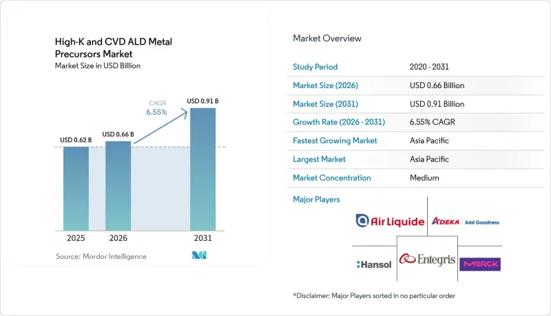
根據 Mordor Intelligence 預測,高介電常數和 CVD ALD 金屬前驅體的市場規模預計將從 2025 年的 6.2 億美元成長到 2026 年的 6.6 億美元,到 2031 年達到 9.1 億美元,2026 年至 2031 年的複合年成長率為 6.5%。
本報告按金屬類型(鉿、鋯、鋁、鈷、鎢等)、沉積方法(熱原子層沉積、等離子體增強原子層沉積等)、形態(液態前驅體、固體前驅體、氣態前驅體)、最終用途(邏輯裝置FinFET/GAA、記憶體DRAM、3D NAND等)和地區進行細分。市場預測以美元計價。
全球高介電常數及化學氣相沉積金屬前驅體市場趨勢及洞察
主流小型化技術正朝著小於3nm的邏輯節點發展。
在2奈米節點的環柵(GAA)奈米片設計中,環繞式閘極和背面電源網路使所需的原子層沉積(ALD)循環次數翻倍,導致每片晶圓上的高介電常數絕緣體數量比3奈米FinFET多35%至50%。台積電的N2邏輯元件將於2025年底開始量產,該元件將在裝置堆疊的兩側沉積氧化鉿;而英特爾的18A PowerVia製程將在前驅體材料清單中添加鎢穿透矽通孔。由此導致的前驅體用量激增將因「良率學習過剩」而進一步加劇,迫使晶圓廠在初始量產階段過度供應材料。
背面電源的逐層控制
背面電源佈線需要在直徑小於 500 奈米的穿透矽通孔(TSV) 上採用原子層沉積 (ALD) 技術沉積釕或鎢。這些材料至關重要,因為它們即使在如此微小的尺度下也能保持性能。在英特爾的 18A 節點中,之所以選擇釕,是因為其低電阻率可最大限度地減少能量損耗,並且其優異的抗電遷移性能可增強在高電流密度下的耐久性。此外,Imec 的研究表明,採用背面電源佈線可以將片上電壓降降低約 25%,從而提高整體供電效率。然而,雖然這種佈局顯著降低了 IR 壓降,但預計會使每片晶圓的前驅體材料成本增加 40%,因此需要在性能提升和製造成本之間進行權衡。
鉿金屬供應限制和價格波動
與鋯礦開採密切相關的鉿產量在2025年僅為80-90噸。然而,預計到2028年,鉿前驅體的需求將超過120噸,造成巨大的供需缺口。這種供需失衡導致現貨價格飆升,在2026年第一季達到每公斤1,400美元。價格飆升迫使半導體晶圓廠增加庫存並維持更大的安全庫存,以降低供應風險。雖然預計到2027年西澳大利亞新增的分離產能將增加15-20噸,但這僅能緩解預期供不應求的一小部分,滿足不斷成長的需求的市場壓力預計仍將持續。
細分市場分析
預計到2025年,鎢基化學品將佔據最大的市場佔有率,達到45.74%。其主導地位主要得益於鎢基化學品在接觸插頭和字線中的重要作用,在這些應用中,低電阻率和高模量至關重要。用於高介電常數材料以及鎢基材料在化學氣相沉積(CVD)和原子層沉積(ALD)應用中的金屬前驅體市場,到2025年將佔總收入的近一半,這反映出它們在邏輯和儲存堆疊中的廣泛應用。同時,釕因其即使在厚度小於5奈米的情況下仍具有良好的電阻率而備受關注,並且新型液態前驅體能夠實現超過100託的穩定蒸氣壓。鋯的複合年成長率(CAGR)為6.98%,這顯示鐵電HfZrO<sub>3</sub>介電材料正在改變嵌入式記憶體的發展模式。
隨著代工廠將鐵電場效電晶體(FeFET)整合到整個微控制器節點中,鋯的市場佔有率可能會蠶食鎢的佔有率。鉿仍然是一種戰略金屬,因為所有7奈米以下的閘極介質都依賴它,但其供應鏈結構性緊張。 PowerVia的風險生產案例表明,釕在背面電源軌襯墊中的應用日益廣泛,這預示著材料成分正在顛覆性轉變。鈷和鉬作為阻擋層襯墊的替代材料,正在發揮雖小但日益重要的作用,而氧化鋁在成熟的模擬和功率裝置中仍然佔據著重要地位。
由於製程簡單,熱原子層沉積(ALD)技術預計到2025年將保持48.19%的最大市場佔有率,但等離子體增強型ALD技術7.11%的複合年成長率表明,長寬比限制正在重塑設備發展藍圖。預計在預測期的後半段,用於高介電常數(High-K)和化學氣相沉積(CVD)的等離子體增強型ALD技術的金屬前驅體市場規模將超過熱製程的銷售額,因為DRAM溝槽和背面通孔都需要遠端等離子體化學處理。與13.56 MHz系統相比,超高頻等離子體源可將離子損傷降低一半,並擴大製程窗口,使其適用於對介電常數要求不高、對材料要求不高的堆疊結構。
金屬有機化學氣相沉積(MOCVD)憑藉其每分鐘5-10奈米的沉積速率,在厚鎢填料和鋁焊盤的製備中繼續發揮著至關重要的作用,從而降低了大規模生產結構中晶圓的單片成本。太空原子層沉積(ALD)和混合ALD-CVD製程目前仍處於少數,但因其連續運行和順序成核的優勢,正受到顯示器、太陽能電池和先進封裝用戶的關注。英特爾宣布推出用於18A通孔的混合ALD種子+CVD塊狀鎢製備方法,顯示這些混合製程正變得越來越普及。
區域分析
亞太地區憑藉韓國、台灣和中國龐大的晶圓產能,預計2025年將佔全球60.28%的市佔率。 2024年至2026年間,該地區晶圓廠投資額將超過2,000億美元,預計2031年,年複合成長率將達到7.21%。三星重啟P5計畫以及SK海力士龍仁工廠建設的加速推進,迫使供應商確保本地庫存。與此同時,長江儲存和長江儲存正在加速擴張以應對出口限制。強而有力的政策支持、穩定的勞動力以及完善的產業生態系統,使得亞太地區即使在當地工資水準不斷上漲的情況下,也能維持成本優勢。
到2025年,北美將佔全球銷售額的近19%,並有望實現約7%的複合年成長率。 《晶片法案》(CHIPS Act)的獎勵鼓勵至少23座新晶圓廠的建設或擴建。台積電位於亞利桑那州的工廠、英特爾位於俄亥俄州的工廠以及三星位於德克薩斯的工廠都需要當地的鉿和鎢精煉廠來滿足國內採購需求。液化空氣集團、安特格里斯集團和SK材料集團已開始在這些大型企劃附近建造氣體和前驅體製造地。
受英特爾馬格德堡工廠和義法半導體克羅勒工廠擴建計畫的推動,歐洲在2025年的支出比例將達到約11%。憑藉汽車產業的需求以及國內採購舉措帶來的補貼,該地區正以約6%的複合年成長率成長。中東、非洲和南美洲的總合仍低於5%,但巴西的汽車製造廠和以色列的國防相關設施預計將為高利潤特種產品帶來商機。在所有地區,由於雙重採購和更短的前置作業時間,擁有多家ISO認證工廠的供應商正逐漸獲得競爭優勢。
其他好處:
- Excel格式的市場預測(ME)表
- 3個月的分析師支持
目錄
第1章:引言
- 研究假設和市場定義
- 調查範圍
第2章:調查方法
第3章執行摘要
第4章 市場狀況
- 市場概覽
- 市場促進因素
- 主流小型化技術正朝著小於3nm的邏輯節點發展。
- 透過對每一層的原子級控制實現背面供電
- 超過 500 層的 3D-NAND 堆疊推動了對 ALD 前驅體的需求。
- 採用極紫外光刻技術製備的高長寬比DRAM溝槽電容器
- 《晶片製造和整合法案》(CHIPS Act)通過後,中國、韓國和美國的晶片叢集迅速擴張。
- 用於物聯網邊緣應用的嵌入式非揮發性記憶體的鐵電HfZrO裝置
- 市場限制因素
- 鉿金屬供應限制和價格波動
- 加強對烷基醯胺和 PFAS 配體化學品的環境、健康與安全 (EHS) 法規
- 固體前驅體昇華及供應系統的資本投資強度
- 等離子體損傷造成的缺陷會縮小 PE-ALD 製程的適用範圍。
- 產業價值鏈分析
- 宏觀經濟因素對市場的影響
- 監理情勢
- 技術展望
- 波特五力分析
第5章 市場規模與成長預測
- 按金屬類型
- 鉿
- 鋯
- 鋁
- 鈷
- 鎢
- 釕
- 其他金屬類型
- 透過成膜法
- 熱原子層沉積
- 等離子體增強原子層沉積
- 金屬有機化學氣相沉積
- 空間ALD
- 混合ALD-CVD
- 按形式
- 液態前驅體
- 固體前驅體
- 氣體前驅體
- 按最終用途
- 邏輯裝置,FinFET/GAA
- 內存,DRAM
- 記憶體,3D NAND
- 新興儲存技術(RRAM、MRAM、Fe-FET)
- 佈線和金屬化
- 類比、電源和專用設備
- 按地區
- 北美洲
- 南美洲
- 歐洲
- 亞太地區
- 中東
- 非洲
第6章 競爭情勢
- 市場集中度
- 策略趨勢
- 市佔率分析
- 公司簡介
- Air Liquide SA
- ADEKA Corporation
- Merck KGaA
- Entegris Inc.
- Hansol Chemical Co., Ltd.
- DNF Co., Ltd.
- Soulbrain Co., Ltd.
- UP Chemical Co., Ltd.
- Tanaka Kikinzoku Kogyo KK
- Strem Chemicals, Inc.
- Versum Materials LLC
- SK Trichem Co., Ltd.
- SK Materials Co., Ltd.
- Gelest, Inc.
- Air Products and Chemicals, Inc.
- Jiangsu Yoke Technology Co., Ltd.
- Solvay SA
- Nanmat Technology Co., Ltd.
- Mecaro Co., Ltd.
- EpiValence Ltd.
- American Elements
- Botai Electronic Material Co., Ltd.
第7章 市場機會與未來展望
According to Mordor Intelligence, the high-K and CVD ALD metal precursors market size is expected to increase from USD 0.62 billion in 2025 to USD 0.66 billion in 2026 and reach USD 0.91 billion by 2031, growing at a CAGR of 6.55% over 2026-2031.
This report is Segmented by Metal Type (Hafnium, Zirconium, Aluminum, Cobalt, Tungsten, and More), Deposition Method (Thermal ALD, Plasma-Enhanced ALD, and More), Form (Liquid Precursors, Solid Precursors, and Gas Precursors), End-Use Application (Logic Devices FinFET/GAA, Memory DRAM, Memory 3D NAND, and More ), and Geography. The Market Forecasts are Provided in Terms of Value (USD).
Global High-K And CVD ALD Metal Precursors Market Trends and Insights
Mainstream Scaling to Sub-3 nm Logic Nodes
Gate-all-around nanosheet designs at 2-nanometer nodes consume 35-50% more high-k dielectric per wafer than 3-nanometer FinFETs because wrap-around gates and backside power networks double the number of ALD cycles required. TSMC's N2 logic, in volume production since late 2025, deposits hafnium oxide on both sides of the device stack, while Intel's 18A PowerVia flow adds tungsten through-silicon vias to the precursor bill of materials. The resulting spike in precursor intensity is magnified by yield-learning overruns that force fabs to over-provision materials during early ramps.
Layer-by-Layer Control for Backside Power Delivery
Backside power routes require ruthenium or tungsten atomic layer deposition (ALD) on through-silicon vias (TSVs) with diameters less than 500 nanometers. These materials are critical because they can maintain performance at such small scales. Intel's 18A node specifically selected ruthenium because of its low resistivity, which minimizes energy loss, and its superior electromigration resistance, which enhances durability under high current densities. Additionally, research from Imec highlights that adopting backside power routing can reduce on-chip voltage droop by approximately 25%, improving overall power delivery efficiency. However, while this layout significantly reduces IR drop, it also increases the cost of per-wafer precursor materials by an estimated 40%, presenting a trade-off between performance gains and manufacturing expenses.
Hafnium Metal Supply Constraints and Price Volatility
Hafnium output, which is intrinsically linked to zirconium mining, remained limited to only 80-90 metric tons in 2025. However, the demand for hafnium precursors is projected to exceed 120 metric tons by 2028, creating a significant supply-demand gap. This imbalance has driven spot prices to surge, reaching USD 1,400 per kilogram in the first quarter of 2026. The rising prices have compelled semiconductor fabs to increase their inventories and maintain higher safety stocks to mitigate supply risks. Although new separation capacity in Western Australia is expected to add 15-20 metric tons by 2027, this increase will address only a fraction of the anticipated shortfall, leaving the market under pressure to meet growing demand.
Other drivers and restraints analyzed in the detailed report include:
- 3D NAND Stacks Above 500 Layers
- EUV-Patterned High-Aspect-Ratio DRAM Capacitors
- Escalating EHS Regulations on Alkyl-Amide and PFAS Ligand Chemistries
For complete list of drivers and restraints, kindly check the Table Of Contents.
Segment Analysis
Tungsten-based chemistries accounted for the largest share with 45.74% in 2025 value, and that dominance rests on their entrenched role in contact plugs and word-lines, where low resistivity and high modulus are vital. The High-K and Chemical Vapor Deposition (CVD) Atomic Layer Deposition (ALD) metal precursors market for tungsten applications accounted for nearly half of overall revenue in 2025, reflecting widespread integration in both logic and memory stacks. Ruthenium, however, is gaining mindshare because its resistivity remains favorable at sub-5-nanometer thicknesses, and new liquid precursors now deliver stable vapor pressures above 100 torr. Zirconium's 6.98% CAGR shows how ferroelectric HfZrO dielectrics are reshaping embedded memory flows.
Looking forward, zirconium's share acceleration could edge into tungsten territory as foundries deploy FeFETs across microcontroller nodes. Hafnium remains a strategic metal because every sub-7 nanometer gate dielectric relies on it, yet its supply chain is structurally tight. Ruthenium's emergence in backside power rail liners, validated by PowerVia risk production, points to a disruptive mix shift. Cobalt and molybdenum occupy niche but growing roles as barrier-liner substitutes, while aluminum oxide stays relevant for mature analog and power devices.
Thermal ALD retained the largest market share at 48.19% in 2025, thanks to its simplicity, but plasma-enhanced ALD's 7.11% CAGR highlights how aspect-ratio pressures are rewriting tool roadmaps. The High-K and CVD ALD metal precursors market size for plasma-enhanced processes is on track to overtake thermal revenue late in the forecast window as DRAM trenches and backside vias both demand remote-plasma chemistries. Very-high-frequency plasma sources cut ion damage in half compared with 13.56 MHz systems, broadening the process window for sensitive low-k stacks.
Metal-organic CVD still underpins thick tungsten fills and aluminum pads because its 5-10 nanometer-per-minute deposition rates keep the cost-per-wafer low for high-volume structures. Spatial ALD and hybrid ALD-CVD flows remain minority shares but are attracting display, solar, and advanced packaging users who value the advantages of continuous motion or sequential nucleation. Intel's public disclosure of a hybrid ALD-seed plus CVD-bulk tungsten approach for 18A vias signals broader acceptance of these mixed regimes.
Geography Analysis
Asia-Pacific dominates value with a 60.28% hold in 2025, reflecting massive wafer capacity across Korea, Taiwan, and China. Regional fab investments exceeding USD 200 billion between 2024-2026 underpin a 7.21% CAGR to 2031. Samsung's restarted P5 project and SK hynix's advanced Yongin timeline force suppliers to pre-position inventory on site, while YMTC and CXMT accelerate expansions to counter export controls. Strong policy support, labor availability, and entrenched ecosystems allow the Asia-Pacific to maintain cost advantages despite a rising local wage base.
North America accounted for close to 19% of 2025 revenue and is on track for roughly a 7% CAGR as CHIPS Act incentives trigger at least 23 new fabs or expansions. TSMC Arizona, Intel Ohio, and Samsung Texas collectively require localized hafnium and tungsten purification plants to satisfy domestic-content mandates. Air Liquide, Entegris, and SK Materials are already breaking ground on gas and precursor campuses adjacent to these megaprojects.
Europe controls about 11% of 2025 spend, buoyed by Intel Magdeburg and STMicroelectronics Crolles expansions. Regional growth hovers near 6% CAGR as automotive demand and sovereignty initiatives lock in subsidies. The Middle East, Africa, and South America remain sub-5% combined, yet Brazilian automotive fabs and Israeli defense nodes present high-margin specialty opportunities. Across all regions, dual sourcing and shorter lead-times shift competitive advantage toward suppliers operating multiple ISO-certified plants.
- Air Liquide S.A.
- ADEKA Corporation
- Merck KGaA
- Entegris Inc.
- Hansol Chemical Co., Ltd.
- DNF Co., Ltd.
- Soulbrain Co., Ltd.
- UP Chemical Co., Ltd.
- Tanaka Kikinzoku Kogyo K.K.
- Strem Chemicals, Inc.
- Versum Materials LLC
- SK Trichem Co., Ltd.
- SK Materials Co., Ltd.
- Gelest, Inc.
- Air Products and Chemicals, Inc.
- Jiangsu Yoke Technology Co., Ltd.
- Solvay S.A.
- Nanmat Technology Co., Ltd.
- Mecaro Co., Ltd.
- EpiValence Ltd.
- American Elements
- Botai Electronic Material Co., Ltd.
Additional Benefits:
- The market estimate (ME) sheet in Excel format
- 3 months of analyst support
TABLE OF CONTENTS
1 INTRODUCTION
- 1.1 Study Assumptions and Market Definition
- 1.2 Scope of the Study
2 RESEARCH METHODOLOGY
3 EXECUTIVE SUMMARY
4 MARKET LANDSCAPE
- 4.1 Market Overview
- 4.2 Market Drivers
- 4.2.1 Mainstream Scaling to Sub-3 nm Logic Nodes
- 4.2.2 Layer-by-Layer Atomic-Scale Control Enabling Backside Power Delivery
- 4.2.3 3D-NAND Stacks Above 500 Layers Multiplying ALD Precursor Volumes
- 4.2.4 EUV-Patterned High-Aspect-Ratio DRAM Trench Capacitors
- 4.2.5 Rapid Build-Out of Chinese, Korean and US Fab Clusters Post-CHIPS Acts
- 4.2.6 Ferroelectric HfZrO Devices for Embedded Non-Volatile Memory in IoT Edge
- 4.3 Market Restraints
- 4.3.1 Hafnium Metal Supply Constraints and Price Volatility
- 4.3.2 Escalating EHS Regulations on Alkyl-Amide and PFAS Ligand Chemistries
- 4.3.3 Capex Intensity of Solid-Precursor Sublimation and Delivery Systems
- 4.3.4 Plasma Damage-Induced Defectivity Narrowing PE-ALD Process Windows
- 4.4 Industry Value-Chain Analysis
- 4.5 Impact of Macroeconomic Factors on the Market
- 4.6 Regulatory Landscape
- 4.7 Technological Outlook
- 4.8 Porter's Five Forces Analysis
- 4.8.1 Threat of New Entrants
- 4.8.2 Bargaining Power of Suppliers
- 4.8.3 Bargaining Power of Buyers
- 4.8.4 Threat of Substitutes
- 4.8.5 Intensity of Competitive Rivalry
5 MARKET SIZE AND GROWTH FORECASTS (VALUE)
- 5.1 By Metal Type
- 5.1.1 Hafnium
- 5.1.2 Zirconium
- 5.1.3 Aluminum
- 5.1.4 Cobalt
- 5.1.5 Tungsten
- 5.1.6 Ruthenium
- 5.1.7 Other Metal Type
- 5.2 By Deposition Method
- 5.2.1 Thermal ALD
- 5.2.2 Plasma-Enhanced ALD
- 5.2.3 Metal-Organic CVD
- 5.2.4 Spatial ALD
- 5.2.5 Hybrid ALD-CVD
- 5.3 By Form
- 5.3.1 Liquid Precursors
- 5.3.2 Solid Precursors
- 5.3.3 Gas Precursors
- 5.4 By End-Use Application
- 5.4.1 Logic Devices, FinFET/GAA
- 5.4.2 Memory, DRAM
- 5.4.3 Memory, 3D NAND
- 5.4.4 Emerging Memory (RRAM, MRAM, Fe-FET)
- 5.4.5 Interconnects and Metallization
- 5.4.6 Analog, Power and Specialty Devices
- 5.5 By Geography
- 5.5.1 North America
- 5.5.2 South America
- 5.5.3 Europe
- 5.5.4 Asia-Pacific
- 5.5.5 Middle East
- 5.5.6 Africa
6 COMPETITIVE LANDSCAPE
- 6.1 Market Concentration
- 6.2 Strategic Moves
- 6.3 Market Share Analysis
- 6.4 Company Profiles (includes Global Level Overview, Market Level Overview, Core Segments, Financials as available, Strategic Information, Market Rank/Share, Products and Services, Recent Developments)
- 6.4.1 Air Liquide S.A.
- 6.4.2 ADEKA Corporation
- 6.4.3 Merck KGaA
- 6.4.4 Entegris Inc.
- 6.4.5 Hansol Chemical Co., Ltd.
- 6.4.6 DNF Co., Ltd.
- 6.4.7 Soulbrain Co., Ltd.
- 6.4.8 UP Chemical Co., Ltd.
- 6.4.9 Tanaka Kikinzoku Kogyo K.K.
- 6.4.10 Strem Chemicals, Inc.
- 6.4.11 Versum Materials LLC
- 6.4.12 SK Trichem Co., Ltd.
- 6.4.13 SK Materials Co., Ltd.
- 6.4.14 Gelest, Inc.
- 6.4.15 Air Products and Chemicals, Inc.
- 6.4.16 Jiangsu Yoke Technology Co., Ltd.
- 6.4.17 Solvay S.A.
- 6.4.18 Nanmat Technology Co., Ltd.
- 6.4.19 Mecaro Co., Ltd.
- 6.4.20 EpiValence Ltd.
- 6.4.21 American Elements
- 6.4.22 Botai Electronic Material Co., Ltd.
7 MARKET OPPORTUNITIES AND FUTURE OUTLOOK
- 7.1 White-Space and Unmet-Need Assessment
 全球高介電常數和CVD/ALD金屬前驅體市場規模、佔有率、趨勢和成長分析報告,2026-2034年
 高介電常數和 CVD/ALD 金屬前驅體市場規模、佔有率和成長分析:按產品類型、沉積技術、應用、材料類型、最終用戶、純度等級和地區分類—2026-2033 年產業預測
 高介電常數和化學氣相沉積原子層沉積金屬前驅體市場:按技術、應用和地區分類(2026-2034 年)
 高介電常數和化學氣相沉積金屬前驅體市場:按技術、材料類型、功能、應用、終端用戶產業和分銷管道分類-2026年至2032年全球市場預測
 高介電常數和化學氣相沉積(CVD)鋁金屬前驅體市場-全球產業規模、佔有率、趨勢、機會、預測:按技術、應用、區域和競爭對手分類,2021-2031年前驅體材料市場按類型、純度、等級、形態、應用和最終用途產業分類-2026年至2032年全球預測高介電常數金屬閘極技術市場:依元件類型、製程節點、製造技術、材料類型與最終用途應用分類-2026-2032年全球預測
 全球前驅材料市場
 前驅體材料市場,按類型、應用、國家和地區 - 2024-2032 年行業分析、市場規模、市場佔有率和預測全球高 k 和 CVD ALD 金屬前驅物市場研究報告 - 2024 年至 2032 年產業分析、規模、佔有率、成長、趨勢和預測