


 |
市場調查報告書
商品編碼
2062307
輪廓儀:市場佔有率分析、行業趨勢和統計數據、成長預測(2026-2031 年)Profilometer - Market Share Analysis, Industry Trends & Statistics, Growth Forecasts (2026 - 2031) |
||||||

※ 本網頁內容可能與最新版本有所差異。詳細情況請與我們聯繫。
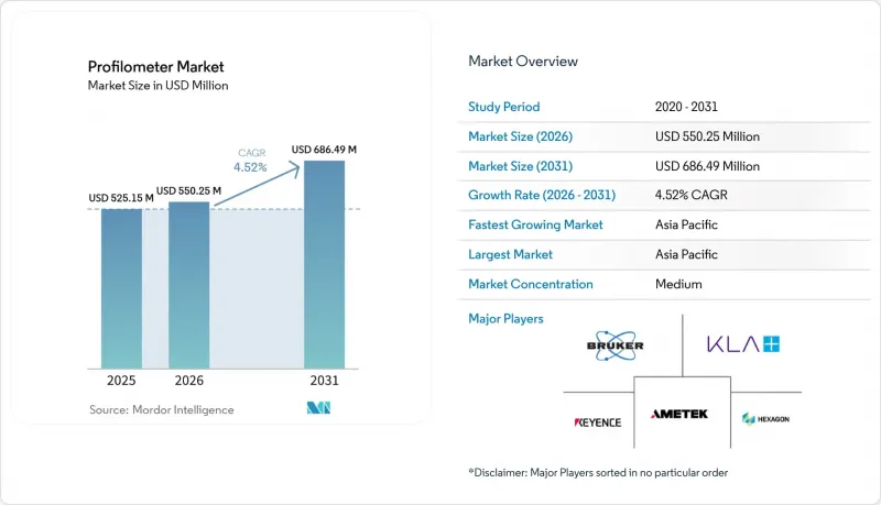
預計輪廓儀市場將從 2025 年的 5.2515 億美元成長到 2026 年的 5.5025 億美元,到 2031 年達到 6.8649 億美元,2026 年至 2031 年的複合年成長率預計為 4.52%。
本報告按技術(接觸式觸針輪廓儀、白光干涉輪廓儀等)、測量尺寸(2D輪廓測量等)、外形規格(桌上型/實驗室系統、線上/機載系統、可攜式/手持式系統)、終端應用產業(半導體及電子、汽車、其他)和地區進行細分。市場預測以美元計價。
全球輪廓儀市場趨勢與洞察
半導體製造中對精確表面特性評估的需求日益成長
對於2nm以下的邏輯節點和混合鍵結互連,晶圓廠需要將晶圓粗糙度控制在0.3nm Rq或更低,以抑制空洞和閾值電壓漂移。隨著台灣和韓國在2025年產能擴張後引入線上白光干涉儀,廢品率已降低15 % ,這反映了輪廓儀市場在封閉回路型CMP控制的提案。相移演算法、隔離表和可追溯的ISO 25178-604校準參考件,可實現300mm晶圓上埃級重複性,滿足代工廠審核要求,並增強廠商鎖定。
向非接觸式和3D輪廓測量技術過渡
光學輪廓測量技術可消除軟塗層和脆弱奈米結構中的觸針變形。 Sensofar 的多感測器「S Neox 五軸」平台可讓使用者在掃描過程中切換共焦、焦點變化和乾涉儀模式,從而將航太渦輪葉片的偵測時間縮短 40% [2]。美國國家標準與技術研究院 (NIST) 的積層製造研究表明,腔內共焦感測器可以在不中斷製造過程的情況下,以 10µm 的解析度繪製每個粉末床層的分佈圖,並實現即時雷射功率校正。
對先進3D光學系統的大量資本投入
具備自動拼接功能的測量干涉儀售價超過30萬美元,成為其普及應用的一大障礙,尤其對中小企業而言更是如此。如此高昂的成本往往使得中小企業難以證明投資的合理性,除非能夠獲得清晰且可衡量的回報。 Polytech公司的Pro.Surf+就是一個典型的例子。這類企業的採購委員會在批准大額支出之前,通常會要求提供詳細的投資報酬率(ROI)分析,特別是與可量化的缺陷減少相關的分析。這種嚴格的財務審查凸顯了中小企業在採用先進測量解決方案時所面臨的困境,儘管這些方案具有潛在的巨大收益。
細分市場分析
2025年,白光干涉測量技術佔輪廓儀銷售額的41.75%,其在TSV深度和MEMS台階高度方面實現了亞奈米級精度,從而推動了輪廓儀市場的發展。隨著製造商對具有多個傾斜角度的多層結構在線環境下的檢測需求不斷成長,色散共焦和條紋投影解決方案預計將以每年5.23%的速度成長至2031年,高於市場平均水平。預計到2031年,干涉測量輪廓儀市場規模將擴大至2.7億美元,而共焦輪廓儀細分市場預計將達到1.85億美元,在不取代現有設備的情況下縮小兩者之間的差距。
Zygo 和Keyence的第二代多感測器探頭將干涉測量、共聚焦顯微鏡和聚焦調節等先進技術整合到一個緊湊的封裝中。這種整合顯著減少了對大規模培訓的需求,並使高混合生產設施能夠在統一的平台上採用和標準化操作。此外,這種標準化提高了客戶的轉換成本,這對於維持和提高輪廓儀市場的供應商利潤率至關重要。
預計到2025年,3D表面測量系統將佔據58.31%的市場佔有率,年成長率為5.11%。這反映了ISO 25178標準的全球標準化以及Sa、Svk和峰值材料體積等測量指標的統計穩健性。表面測量標準正被應用於汽車搪光、整形外科植入紋理化和電動汽車電池電極等領域,加速了輪廓儀市場佔有率從2D測試向3D測試的轉變。雖然2D輪廓儀在高通量合格/不合格判定方面仍佔有一席之地,但2026年至2028年的大部分新增資本投資將流向具備表面測量功能的平台。
基於雲端的GPU分析技術可在短短幾秒鐘內處理1000萬張高程圖,從而實現即時決策循環並促進無縫遠端協作。這項技術進步正將市場需求從專注於硬體解決方案的供應商轉向提供強大軟體生態系統的供應商。這種轉變進一步提高了高程剖面儀市場的進入門檻,使新參與企業越來越難以立足。
區域分析
預計到2025年,亞太地區將佔全球銷售額的37.53%,並在2031年之前維持4.38%的複合年成長率。這主要得益於台灣和韓國500億美元的鑄造廠擴建投資,這些擴建項目將引入用於化學機械拋光(CMP)和混合鍵合控制的輪廓儀。在中國當地,國家積體電路基金提供的150億美元測量技術支援計畫正在推動干涉儀在國內的應用,儘管在最高解析度方面仍落後於老牌製造商。印度的電子產品生產連結獎勵計畫計劃(PLI)強制要求實驗室獲得ISO 17025認證,推動了班加羅爾和普納等地對輪廓儀的需求。
預計到2025年,北美將佔全球需求的約28%,這主要得益於價值520億美元的美國晶片製造和生產法案(CHIPS Act)以及波音和空中巴士兩大航太供應鏈的推動。英特爾、美光以及其他全球晶圓代工廠計劃在2027年前投產,並將部署線上輪廓測量系統,以確保良率並為中期成長奠定基礎。在加拿大魁北克的航太中心,可攜式輪廓測量儀是進行飛行中檢測的首選設備。同時,在墨西哥,電動車動力總成市場的蓬勃發展正推動一級供應商的採購。
預計到2025年,歐洲將佔全球銷售額的約25%。其中,德國投資100億歐元(113億美元)用於電動車生產線,這些生產線旨在定義電池電極的表面紋理;法國航太叢集正在實施NADCAP表面審核;歐盟晶片立法部門投資430億歐元(486億美元)用於半導體製造廠,這些工廠大量使用測量儀器。儘管DIN EN ISO 21920、AMS2700和SEMI M59等標準的分散性使歐洲各地的採購變得複雜,但將於2024年最終確定的ISO 10360光學驗收測試提供了一個通用的檢驗標準,並正在推動其在整個歐洲大陸的普及應用。
其他好處:
- Excel格式的市場預測(ME)表
- 3個月的分析師支持
目錄
第1章:引言
- 研究假設和市場定義
- 調查範圍
第2章:調查方法
第3章執行摘要
第4章 市場狀況
- 市場概覽
- 市場促進因素
- 半導體製造中對精密表面性能評估的需求日益成長。
- 不同終端用戶產業對品管和表面檢測的需求
- 向非接觸式和3D輪廓測量技術過渡
- 與自動化和智慧製造的整合
- 採用輪廓儀對積層製造過程中的原位監測進行應用。
- 量子計算硬體製造領域對錶面測量技術的新需求。
- 市場限制因素
- 對先進3D光學系統的大量資本投入
- 各種表面測量技術正在爭奪市場佔有率。
- 各行業面積紋理參數標準化的局限性
- 對稀土元素光學元件的供應鏈不穩定
- 產業供應鏈分析
- 宏觀經濟因素對市場的影響
- 監理情勢
- 技術展望
- 波特五力分析
第5章 市場規模與成長預測
- 透過技術
- 接觸式觸針輪廓儀
- 白光干涉輪廓儀
- 共聚焦雷射掃描輪廓儀
- 色散共聚焦條紋投影輪廓儀
- 按測量軸
- 2D輪廓測量
- 3D表面輪廓測量
- 按外形規格
- 桌上型/實驗室系統
- 線上/機上系統
- 可攜式/手持系統
- 產業最終用途
- 半導體和電子學
- 車
- 航太/國防
- 衛生保健
- 製造業
- 能源與電力
- 按地區
- 北美洲
- 美國
- 加拿大
- 墨西哥
- 歐洲
- 英國
- 德國
- 法國
- 義大利
- 其他歐洲國家
- 亞太地區
- 中國
- 日本
- 印度
- 其他亞太國家
- 南美洲
- 巴西
- 其他南美國家
- 中東
- 沙烏地阿拉伯
- 阿拉伯聯合大公國
- 其他中東國家
- 非洲
- 南非
- 奈及利亞
- 其他非洲國家
- 北美洲
第6章 競爭情勢
- Market-Share Analysis
- 公司簡介
- Bruker Corporation
- KLA Corporation
- Keyence Corporation
- GBS Metrology GmbH
- AMETEK Inc.
- Mahr GmbH
- Mitutoyo Corporation
- Hexagon AB
- Jenoptik AG
- Park Systems Corporation
- Sensofar Tech SL
- Nanovea Inc.
- HORIBA Group
- Polytec GmbH
- Milexia Group
- Paragon Instruments
- Intertek Group plc
- Zygo Corporation
- Trimos SA
- Veeco Instruments Inc.
第7章 市場機會與未來展望
According to Mordor Intelligence, the profilometer market size is expected to increase from USD 525.15 million in 2025 to USD 550.25 million in 2026 and reach USD 686.49 million by 2031, growing at a CAGR of 4.52% over 2026-2031.
This report is Segmented by Technology (Contact-Stylus Profilometers, White-Light Interferometry Profilometers, and More), Measurement Dimension (2-D Profilometry, and More), Form Factor (Benchtop/Lab Systems, In-Line/On-Machine Systems, and Portable/Hand-Held Systems), End-Use Industry (Semiconductor and Electronics, Automotive, and More), and Geography. The Market Forecasts are Provided in Terms of Value (USD).
Global Profilometer Market Trends and Insights
Rising Demand for Precision Surface Characterization in Semiconductor Manufacturing
Sub-2 nm logic nodes and hybrid-bonding interconnects require fabs to control wafer roughness to below 0.3 nm Rq to suppress voids and threshold-voltage shifts. Inline white-light interferometers installed in Taiwan and South Korea during 2025 capacity expansions have cut scrap by 15%, validating the profilometer market's value proposition for closed-loop CMP control. Phase-shifting algorithms, isolation tables, and traceable ISO 25178-604 calibration artifacts allow angstrom-level repeatability across 300 mm wafers, satisfying foundry audit requirements and reinforcing vendor lock-in.
Shift Toward Non-Contact and 3D Profilometry Technologies
Optical profilometry eliminates stylus-induced deformation on soft coatings and fragile nanostructures. Sensofar's multi-sensor S Neox Five Axis platform lets users toggle among confocal, focus-variation, and interferometry modes mid-scan, reducing inspection time 40% for aerospace turbine blades[2].NIST's additive-manufacturing study proved in-chamber confocal sensors can map each powder-bed layer at 10 µm resolution without pausing the build, enabling real-time laser-power corrections.
High Capital Expenditure of Advanced 3D Optical Systems
Research-grade interferometers with automated stitching cost over USD 300,000, creating a significant barrier to adoption, particularly for small and medium-sized enterprises (SMEs). This high cost often makes it difficult for SMEs to justify the investment without clear, measurable returns. Polytec's Pro.Surf+ serves as a prime example of this issue. Procurement committees within these organizations frequently require a detailed return on investment (ROI) analysis, specifically tied to quantifiable scrap savings, before approving such substantial expenditures. This financial scrutiny highlights the difficulty SMEs face in adopting advanced metrology solutions despite their potential benefits.
Other drivers and restraints analyzed in the detailed report include:
- Quality Control and Surface Inspection Needs Across Diverse End-Use Industries
- Integration With Automation and Smart Manufacturing
- Competing Surface-Metrology Technologies Cannibalizing Share
For complete list of drivers and restraints, kindly check the Table Of Contents.
Segment Analysis
White-light interferometry accounted for 41.75% of 2025 revenue, benefiting the profilometer market through its sub-nm accuracy across TSV depths and MEMS steps. Chromatic confocal and fringe-projection solutions will outpace the market at 5.23% annually through 2031 as manufacturers seek slope-rich, multilayer-friendly inspection in line environments. The profilometer market size for interferometry instruments is projected to expand to USD 270 million by 2031, whereas confocal sub-segments will climb to USD 185 million, narrowing the gap without displacing legacy installs.
Second-generation multi-sensor heads from Zygo and Keyence integrate advanced technologies such as interferometry, confocal microscopy, and focus variation into a single, compact package. This integration significantly reduces the need for extensive training, enabling high-mix manufacturing facilities to adopt and standardize operations on a unified platform. Additionally, this standardization increases switching costs for customers, a critical factor in maintaining and enhancing vendor profit margins in the profilometer market.
Three-dimensional areal systems held a 58.31% share in 2025 and are growing at 5.11% annually, reflecting ISO 25178's global harmonization and the statistical robustness of Sa, Svk, and peak-material-volume metrics. Automotive honing, orthopedic implant texturing, and EV battery electrodes all cite areal standards, accelerating the migration of profilometer market share away from two-dimensional stylus traces. Two-dimensional profilometers retain a foothold in high-throughput go/no-go checks, yet most new capex in 2026-2028 is directed toward areal-capable platforms.
Cloud-based GPU analytics now process 10-million-point height maps in mere seconds, enabling real-time decision-making loops and facilitating seamless remote collaboration. This technological advancement has shifted market demand toward vendors offering robust software ecosystems rather than those focusing solely on hardware solutions. This shift has further strengthened the barriers to entry in the profilometer market, making it increasingly challenging for new competitors to establish a foothold.
Geography Analysis
Asia-Pacific accounted for 37.53% of 2025 revenue and will log a 4.38% CAGR to 2031, buoyed by USD 50 billion in Taiwanese and South Korean foundry expansions that embed profilometers for CMP and hybrid-bond bonding control. Mainland China's USD 15 billion metrology stimulus under its National IC Fund catalyzes domestic interferometer builds, though top-tier resolution still trails incumbents. India's PLI electronics scheme mandates ISO 17025 labs, boosting demand for profilometers across Bengaluru and Pune.
North America accounted for ~28% of 2025 demand, backed by the USD 52 billion U.S. CHIPS Act and the Boeing-Airbus aerospace supply chains. Intel, Micron, and GlobalFoundries plan to open fabs through 2027, with inline profilometer suites to ensure yield and anchor mid-term growth. Canada's Quebec aerospace hub prefers portable profilometers for on-wing inspection, while Mexico's EV drivetrain boom drives purchases among Tier 1 suppliers.
Europe held roughly 25% of 2025 sales, with Germany investing EUR 10 billion (USD 11.3 billion) in EV lines that specify battery-electrode areal texture, France's aerospace cluster enforcing NADCAP surface audits, and the EU Chips Act channeling EUR 43 billion (USD 48.6 billion) into metrology-rich semiconductor fabs. Fragmented standards, DIN EN ISO 21920, AMS2700, SEMI M59, complicate pan-European procurement, but ISO 10360 optical acceptance tests finalized in 2024 now provide common verification tracks, aiding continental adoption.
- Bruker Corporation
- KLA Corporation
- Keyence Corporation
- GBS Metrology GmbH
- AMETEK Inc.
- Mahr GmbH
- Mitutoyo Corporation
- Hexagon AB
- Jenoptik AG
- Park Systems Corporation
- Sensofar Tech SL
- Nanovea Inc.
- HORIBA Group
- Polytec GmbH
- Milexia Group
- Paragon Instruments
- Intertek Group plc
- Zygo Corporation
- Trimos SA
- Veeco Instruments Inc.
Additional Benefits:
- The market estimate (ME) sheet in Excel format
- 3 months of analyst support
TABLE OF CONTENTS
1 INTRODUCTION
- 1.1 Study Assumptions and Market Definition
- 1.2 Scope of the Study
2 RESEARCH METHODOLOGY
3 EXECUTIVE SUMMARY
4 MARKET LANDSCAPE
- 4.1 Market Overview
- 4.2 Market Drivers
- 4.2.1 Rising Demand for Precision Surface Characterization in Semiconductor Manufacturing
- 4.2.2 Quality Control and Surface Inspection Needs Across Diverse End-Use Industries
- 4.2.3 Shift Toward Non-Contact and 3D Profilometry Technologies
- 4.2.4 Integration With Automation and Smart Manufacturing
- 4.2.5 Adoption of Profilometers for In-Situ Monitoring in Additive Manufacturing Processes
- 4.2.6 Emerging Demand for Surface Metrology in Quantum Computing Hardware Fabrication
- 4.3 Market Restraints
- 4.3.1 High Capital Expenditure of Advanced 3D Optical Systems
- 4.3.2 Competing Surface-Metrology Technologies Cannibalizing Share
- 4.3.3 Limited Standardization of Areal Texture Parameters Across Industries
- 4.3.4 Dependency on Rare-Earth Optical Components With Volatile Supply Chains
- 4.4 Industry Supply-Chain Analysis
- 4.5 Impact of Macroeconomic Factors on the Market
- 4.6 Regulatory Landscape
- 4.7 Technological Outlook
- 4.8 Porter's Five Forces Analysis
- 4.8.1 Threat of New Entrants
- 4.8.2 Bargaining Power of Suppliers
- 4.8.3 Bargaining Power of Buyers
- 4.8.4 Threat of Substitutes
- 4.8.5 Competitive Rivalry
5 MARKET SIZE AND GROWTH FORECASTS (VALUE)
- 5.1 By Technology
- 5.1.1 Contact-Stylus Profilometers
- 5.1.2 White-Light Interferometry Profilometers
- 5.1.3 Confocal Laser-Scanning Profilometers
- 5.1.4 Chromatic Confocal and Fringe-Projection Profilometers
- 5.2 By Measurement Dimension
- 5.2.1 2-D Profilometry
- 5.2.2 3-D Areal Profilometry
- 5.3 By Form Factor
- 5.3.1 Benchtop/Lab Systems
- 5.3.2 In-Line/On-Machine Systems
- 5.3.3 Portable/Hand-Held Systems
- 5.4 By End-Use Industry
- 5.4.1 Semiconductor and Electronics
- 5.4.2 Automotive
- 5.4.3 Aerospace and Defence
- 5.4.4 Healthcare
- 5.4.5 Manufacturing
- 5.4.6 Energy and Power
- 5.5 By Geography
- 5.5.1 North America
- 5.5.1.1 United States
- 5.5.1.2 Canada
- 5.5.1.3 Mexico
- 5.5.2 Europe
- 5.5.2.1 United Kingdom
- 5.5.2.2 Germany
- 5.5.2.3 France
- 5.5.2.4 Italy
- 5.5.2.5 Rest of Europe
- 5.5.3 Asia-Pacific
- 5.5.3.1 China
- 5.5.3.2 Japan
- 5.5.3.3 India
- 5.5.3.4 Rest of Asia-Pacific
- 5.5.4 South America
- 5.5.4.1 Brazil
- 5.5.4.2 Rest of South America
- 5.5.5 Middle East
- 5.5.5.1 Saudi Arabia
- 5.5.5.2 United Arab Emirates
- 5.5.5.3 Rest of Middle East
- 5.5.6 Africa
- 5.5.6.1 South Africa
- 5.5.6.2 Nigeria
- 5.5.6.3 Rest of Africa
- 5.5.1 North America
6 COMPETITIVE LANDSCAPE
- 6.1 Market-Share Analysis
- 6.2 Company Profiles (includes Global Level Overview, Market Level Overview, Core Segments, Financials as available, Strategic Information, Market Rank/Share, Products and Services, Recent Developments)
- 6.2.1 Bruker Corporation
- 6.2.2 KLA Corporation
- 6.2.3 Keyence Corporation
- 6.2.4 GBS Metrology GmbH
- 6.2.5 AMETEK Inc.
- 6.2.6 Mahr GmbH
- 6.2.7 Mitutoyo Corporation
- 6.2.8 Hexagon AB
- 6.2.9 Jenoptik AG
- 6.2.10 Park Systems Corporation
- 6.2.11 Sensofar Tech SL
- 6.2.12 Nanovea Inc.
- 6.2.13 HORIBA Group
- 6.2.14 Polytec GmbH
- 6.2.15 Milexia Group
- 6.2.16 Paragon Instruments
- 6.2.17 Intertek Group plc
- 6.2.18 Zygo Corporation
- 6.2.19 Trimos SA
- 6.2.20 Veeco Instruments Inc.
7 MARKET OPPORTUNITIES AND FUTURE OUTLOOK
- 7.1 White-Space and Unmet-Need Assessment


