

 |
市場調查報告書
商品編碼
2062173
晶片鍵合設備:市場佔有率分析、產業趨勢與統計、成長預測(2026-2031)Die Bonder Equipment - Market Share Analysis, Industry Trends & Statistics, Growth Forecasts (2026 - 2031) |
||||||
※ 本網頁內容可能與最新版本有所差異。詳細情況請與我們聯繫。
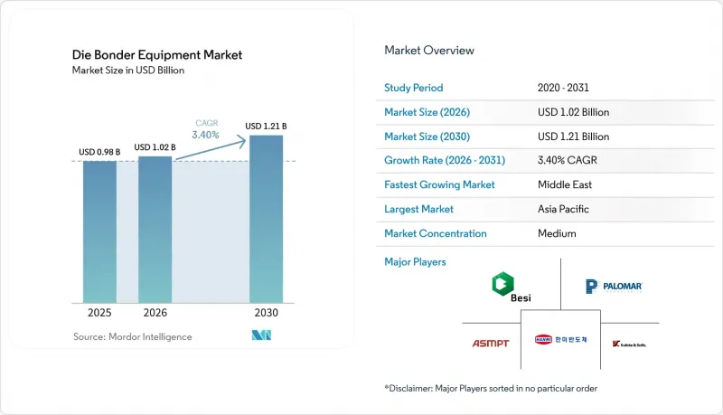
據 Mordor Intelligence 稱,晶片鍵合機設備市場預計將從 2025 年的 9.8 億美元成長到 2026 年的 10.2 億美元,到 2031 年達到 12.1 億美元,2026 年至 2031 年的複合年成長率為 3.40%。
本報告按設備類型(例如,全自動晶片貼裝機)、貼裝技術(例如,環氧樹脂/黏合劑晶片貼裝)、吞吐量(例如,超過 60,000 UPH)、終端用戶行業(例如,整合設備製造商)、裝置類型(例如,邏輯和 IC IC、功率和射頻)以及地區進行細分。市場預測以美元 (USD) 為單位。
全球晶片鍵合機設備市場趨勢及洞察
異質整合與晶片組的蓬勃發展
晶片分割技術將單晶片系統晶片(SoC) 設計分解成更小的晶片單元,並透過細間距的晶片間鏈路連接。這顯著降低了光刻成本並提高了良率,同時也對晶片放置精度提出了更高的要求,即小於 2µm。晶片 CPU 的早期量產證明了其經濟可行性,加速了向熱壓縮平台的轉型,後者只需處理單根鍵合線,而非數十根導線。這提高了設備利用率,並為更高的資本投資提供了合理性。通用晶片互連高速協議 (UCHI-Express) 正在推進協議標準化,擴大晶片鍵合設備市場,並使二線裝置製造商也能使用先進的封裝技術。供應商正在積極回應,推出雙龍門系統、干涉儀感測器和基於機器學習的對準引擎,以縮短設定時間並提高首輪良率。客戶的優勢在於能夠實現靈活組合的設計流程,即使前端小型化速度放緩,也能經濟有效地延續莫耳定律。
採用先進的 2.5D、3D 和混合鍵結技術。
混合鍵合技術在約 200 度C下熔合銅焊盤和介電層,消除了微凸塊,並將連接密度提高到 10,000 個鏈路/mm² 以上。這對於下一代高頻寬記憶體和圖形加速器至關重要。供應商正在共同最佳化晶圓間鍵合機和平面化工藝,以將銅凹陷控制在 5nm 以下,並將套刻誤差控制在 200nm 以下。奈米孿晶銅的應用正在擴展熱製程窗口,從而可以使用有機基板實現精細間距的 3D 堆疊。由於混合鍵結生產線的成本比覆晶生產線高出 50-70%,預計初期應用將集中在能夠透過大規模生產計畫攤提數百萬美元設備的頂級 IDM 和 OSAT 廠商。一旦第五代 HBM 在 2028 年後實現廣泛量產,材料替代浪潮將席捲整個記憶體和邏輯供應鏈,從而加速對混合相容晶片鍵合機的需求。
中型OSAT廠商投資超高精度設備的負擔
晶圓對晶圓鍵合機(套刻精度低於500奈米)的成本在300萬至500萬美元之間,而成熟的覆晶設備成本在100萬至150萬美元之間,這給服務於成本敏感市場的二線供應商帶來了財務壓力。升級相關儀器和無塵室還需要額外花費100萬至200萬美元,而從區域銀行獲得貸款核准可能需要長達九個月的時間,這會延緩擴張計畫。設備訂閱合約可以部分緩解這種負擔,但其中包含的產量保證對於小規模的廠商來說可能難以滿足。因此,頂級和中級OSAT廠商之間的技術差距正在擴大,導致收入集中在先進封裝領域,同時限制了整個產業的普及率。
細分市場分析
全自動系統循環時間小於0.5秒,並整合了視覺、力控和測量功能,正逐漸成為大批量邏輯和記憶體生產線的主流。全自動平台晶片鍵合機的市場規模反映了其在主要IDM和OSAT廠商的高滲透率。半自動設備可處理需要混合工具的功率和高頻封裝,而手動和原型工作站仍在研發領域中發揮重要作用。成長最快的晶圓對晶圓鍵合機無需拾取放置工藝,並透過實現每平方毫米超過10,000個連接點的連接密度,支援3D晶片堆疊的部署。
隨著晶圓代工廠不斷擴展其3D整合生產線,使其月處理能力超過1000片晶圓,對晶圓級設備的需求也日益成長。供應商不再只是追求處理速度,而是透過整合真空處理、CMP介面和線上偵測功能,在製程控制方面實現差異化,從而確保300mm基板上的套刻精度。在需要即時光學回饋的主動對準的光電領域,手動鍵合機仍然至關重要。半自動工具則在汽車模組領域找到了自己的市場定位,兼具柔軟性和成本優勢。
由於覆晶佔據了最大的市場佔有率。隨著混合鍵合技術在2028年後的普及,覆晶鍵合機的市佔率預計將逐漸下降。環氧樹脂鍵合在消費性電子和工業設備中仍然很受歡迎,因為在這些應用中,成本和散熱設計方面的限制比密度更為重要;而共晶鍵結在航太和醫療應用領域則佔據了重要地位,因為在這些應用中,氣密性至關重要。
混合鍵結技術的發展動能取決於記憶體藍圖向直接銅-銅連接方向發展,以實現超過 2 TB/s 的頻寬。供應商正在聯合開發鍵合機和化學機械拋光 (CMP) 工藝,以實現小於 5 奈米的銅凹陷和小於 200 奈米的套刻精度。熱壓技術仍然是一種過渡技術,並且已經在細間距覆晶和高頻模組中取代了回流焊接技術。未來,對成本均衡和更高密度的需求將推動市場佔有率向混合平台轉移,晶片鍵合設備市場中直接銅-銅鍵合工具的市場規模也將擴大。
區域分析
亞太地區佔全球產能的一半以上,這得益於台灣先進的封裝技術、中國的本土化努力以及韓國的記憶體生產基地。美國政府的資金投入正在加速建設多個後端晶圓廠,預計2027年運作,將提振北美地區的設備出貨量。在歐洲,德國和法國正在增加對化合物半導體封裝的投資,以確保電動車和工業驅動系統的供應。中東正在崛起為一個新的投資區域,政府資金正注入到計劃於2028年後開始出貨的組裝廠。
亞太地區的設備供應商受益於接近性優勢、更短的服務週期以及政府津貼在地採購的獎勵。北美地區的採購趨勢偏向於用於混合鍵結和晶圓堆疊的高精度、高度自動化設備。歐洲市場的需求則傾向於用於功率模組的銀燒結和銅夾相容平台。中東地區的訂單著重於包含培訓包的承包生產線,以加速生態系統的建置。南美和非洲仍處於起步階段,目前僅限於學術機構和原型安裝。
產能擴張正在對整個供應鏈產生連鎖反應。光是台灣地區就需要超過50台晶圓鍵合機,而根據美國《晶片製造和整合法案》(CHIPS Act)下的訂單,供應商的訂單已經排到了幾個月之後。中國的新晉參與企業提供的設備價格低於成熟的覆晶設備,但先進設備仍主要由知名的全球品牌供應。半導體供應的本地化迫使供應商擴大本地支援團隊、倉庫和再加工中心,雖然增加了固定成本,但卻減少了客戶的停機時間。
其他好處:
- Excel格式的市場預測(ME)表
- 3個月的分析師支持
目錄
第1章:引言
- 研究假設和市場定義
- 調查範圍
第2章:調查方法
第3章執行摘要
第4章 市場狀況
- 市場概覽
- 市場促進因素
- 異質整合和 Chiplet 繁榮
- 採用先進的2.5D/3D和混合黏合技術
- 化合物半導體功率裝置的快速普及
- 資料中心對光電和共封裝光學元件的需求
- 政府補貼支持後端製造業務回流。
- 工業4.0推動全自動、高產能的鍵結機
- 市場限制因素
- 中型OSAT廠商投資超高精度設備的負擔
- 亞微米級排列可能導致良率降低
- 精密零件供應鏈瓶頸
- 黏接工具快速過時的風險
- 產業供應鏈分析
- 監理情勢
- 技術展望
- 波特五力分析
- 宏觀經濟因素對市場的影響
第5章 市場規模與成長預測
- 依設備類型
- 全自動晶片鍵合機
- 半自動晶片鍵合機
- 手動/原型黏合機
- 晶圓鍵合機
- 透過結合技術
- 環氧樹脂/黏合劑模具觸摸
- 共晶模具連接
- 覆晶(C4/銅柱)
- 熱壓縮和熱超音波
- 混合和直接銅-銅鍵合
- 依處理能力(每小時機器數)
- 超過 60,000 UPH(高速)
- 30-60k UPH(中速)
- 低於 30,000 UPH(低速/高精度)
- 產業最終用途
- 垂直整合設備製造商(IDM)
- 半導體組裝和測試服務 (OSAT)
- 研究與原型實驗室
- 依設備類型
- 邏輯和記憶體積體電路
- 功率和射頻(SiC、GaN)
- 光電/光收發器
- 微機電系統和感測器
- 按地區
- 北美洲
- 美國
- 加拿大
- 墨西哥
- 南美洲
- 巴西
- 阿根廷
- 其他南美國家
- 歐洲
- 德國
- 英國
- 法國
- 義大利
- 西班牙
- 其他歐洲國家
- 亞太地區
- 中國
- 日本
- 韓國
- 印度
- 其他亞太國家
- 中東
- 沙烏地阿拉伯
- 阿拉伯聯合大公國
- 其他中東國家
- 非洲
- 南非
- 其他非洲國家
- 北美洲
第6章 競爭情勢
- 市場集中度
- 策略趨勢
- 市佔率分析
- 公司簡介
- ASMPT Ltd.
- Kulicke and Soffa Industries Inc.
- BE Semiconductor Industries NV
- Hanmi Semiconductor Co., Ltd.
- Palomar Technologies Inc.
- SHINKAWA Ltd.
- Panasonic Holdings Corp.(Factory Solutions)
- SUSS MicroTec SE
- Toray Engineering Co., Ltd.
- TOWA Corporation
- West-Bond Inc.
- MRSI Systems(Mycronic AB)
- Finetech GmbH & Co. KG
- Canon Machinery Inc.
- DIAS Automation(Shenzhen)Co., Ltd.
- F&K Delvotec Bondtechnik GmbH
- Tresky AG
- Hybond Inc.
- Integra Technologies LLC
- EV Group(EVG)
第7章 市場機會與未來展望
According to Mordor Intelligence, the die bonder equipment market size is expected to increase from USD 0.98 billion in 2025 to USD 1.02 billion in 2026 and reach USD 1.21 billion by 2031, growing at a CAGR of 3.40% over 2026-2031.
This report is Segmented by Equipment Type (Fully-Automatic Die Bonders, and More), Bonding Technology (Epoxy/Adhesive Die Attach, and More), Throughput Category (Greater Than 60k UPH, and More), End-Use Industry (Integrated Device Manufacturers, and More), Device Type (Logic and Memory IC, Power and RF, and More), and Geography. The Market Forecasts are Provided in Terms of Value (USD).
Global Die Bonder Equipment Market Trends and Insights
Heterogeneous-Integration and Chiplet Boom
Chiplet partitioning breaks monolithic system-on-chip designs into smaller tiles connected by fine-pitch die-to-die links, slashing reticle cost and improving yield while demanding placement accuracy tighter than 2 µm. Early high-volume shipments of chiplet CPUs validated the economics and triggered a shift from wire bonding toward thermocompression platforms that process one bond instead of dozens of wires, raising tool utilization and justifying higher capital outlays. Universal Chiplet Interconnect Express is standardizing protocols, making advanced packaging accessible to second-tier device makers and expanding the die bonder equipment market. Suppliers are responding with dual-gantry systems, interferometric sensors, and machine-learning alignment engines that cut setup time and improve first-pass yield. The payoff for customers is a mix-and-match design flow that extends Moore's Law economically even as front-end scaling slows.
Advanced 2.5D 3D And Hybrid Bonding Adoption
Hybrid bonding fuses copper pads and dielectric layers at around 200 °C, eliminating microbumps and lifting connection density above 10,000 links mm-2, a prerequisite for next-generation high-bandwidth memory and graphics accelerators. Tool vendors are co-optimizing wafer-to-wafer bonders with planarization steps to keep copper dishing below 5 nm and overlay error under 200 nm. Nanotwinned copper is widening the thermal process window, making organic substrates viable for fine-pitch 3D stacking. Because hybrid-bonding lines cost 50-70% more than flip-chip lines, adoption is initially concentrated at top-tier IDMs and OSATs that can amortize multi-million-dollar tool sets across high-volume programs. Once HBM generation 5 ramps after 2028, a material replacement wave will cascade through memory and logic supply chains, accelerating demand for hybrid-ready die bonders.
Ultra-High-Precision CapEx Burden For Mid-Tier OSATs
A wafer-to-wafer bonder with sub-500 nm overlay costs USD 3-5 million versus USD 1-1.5 million for a mature flip-chip tool, stretching balance sheets at second-tier providers that serve cost-sensitive markets. Ancillary metrology and cleanroom upgrades add another USD 1-2 million, and financing from regional banks can take nine months to approve, delaying expansion plans. Equipment-as-a-service contracts partly offset the burden but come with volume guarantees that smaller players cannot always meet. The result is a widening technology gap between top-tier and mid-tier OSATs, concentrating advanced-packaging revenue and limiting industry-wide adoption speed.
Other drivers and restraints analyzed in the detailed report include:
- Rapid Uptake of Compound-Semiconductor Power Devices
- Data-Center Photonics and Co-Packaged Optics Demand
- Sub-Micron Alignment Yield-Loss Risk
For complete list of drivers and restraints, kindly check the Table Of Contents.
Segment Analysis
Fully automatic systems dominate high-volume logic and memory lines because they deliver sub-0.5 s cycle times and integrate vision, force control, and metrology. The die bonder equipment market size for fully automatic platforms reflects deep penetration among large IDMs and OSATs. Semi-automatic machines serve power and radio-frequency packages that require mixed tooling, while manual and prototype stations stay relevant in R and D. Wafer-to-wafer bonders, growing fastest, eliminate pick-and-place steps and enable connection densities above 10,000 links mm-2, positioning them for 3D chiplet stacks.
Demand for wafer-level machines is rising as foundries scale 3D integration lines capable of more than 1,000 wafers a month. Suppliers bundle vacuum handling, CMP interfaces, and inline inspection to guarantee overlay across 300 mm substrates, differentiating on process control rather than raw speed. Manual bonders remain indispensable for photonics where active alignment with live optical feedback is required. Semi-automatic tools find a niche in automotive modules, balancing flexibility and cost.
Flip-chip, including copper-pillar attach, commands the largest slice thanks to its maturity and compatibility with organic laminates. The die bonder equipment market share for flip-chip is expected to erode slowly as hybrid bonding ramps after 2028. Epoxy attach stays popular in consumer and industrial devices where cost and thermal budget trump density, while eutectic attach secures aerospace and medical applications that mandate hermeticity.
Hybrid bonding's momentum hinges on memory roadmaps that move to direct copper-to-copper links for bandwidth beyond 2 TB s-1. Vendors co-develop bonders and CMP steps to hit <5 nm copper dishing and <200 nm overlay. Thermocompression remains the bridge technology, already displacing solder reflow in fine-pitch flip-chip and radio-frequency modules. Over time, cost parity and density demands will swing share toward hybrid platforms, expanding the die bonder equipment market size for direct Cu-Cu tools.
Geography Analysis
Asia-Pacific anchors more than half of global capacity, underpinned by Taiwan's advanced packaging, China's localization push, and South Korea's memory footprint. Government funding in the United States spurs multiple back-end fabs expected online by 2027, lifting North American equipment shipments. Europe invests in compound-semiconductor packaging in Germany and France to secure supply for electric vehicles and industrial drives. The Middle East emerges as a greenfield investor, channelling sovereign capital into assembly plants slated for first output after 2028.
Tool vendors in Asia-Pacific enjoy proximity advantages, shorter service cycles, and government incentives that subsidize local sourcing. North American purchases skew toward high-precision, high-automation tools compatible with hybrid bonding and wafer-to-wafer stacking. European demand favours silver-sinter and copper-clip compatible platforms for power modules. Middle East orders emphasize turnkey lines bundled with training to expedite ecosystem buildup. South America and Africa remain nascent, limited to academic and prototype installations.
Capacity moves ripple through supply chains: Taiwan's expansion alone requires more than 50 wafer-to-wafer bonders, and U.S. CHIPS Act awards reserve slots at suppliers' months ahead. Chinese entrants undercut pricing on mature flip-chip tools, but advanced equipment still flows mainly from incumbent global brands. Regionalization of semiconductor supply pushes tool vendors to expand local support teams, warehouses, and refurbish centers, raising fixed cost but shortening downtime for customers.
- ASMPT Ltd.
- Kulicke and Soffa Industries Inc.
- BE Semiconductor Industries N.V.
- Hanmi Semiconductor Co., Ltd.
- Palomar Technologies Inc.
- SHINKAWA Ltd.
- Panasonic Holdings Corp. (Factory Solutions)
- SUSS MicroTec SE
- Toray Engineering Co., Ltd.
- TOWA Corporation
- West-Bond Inc.
- MRSI Systems (Mycronic AB)
- Finetech GmbH & Co. KG
- Canon Machinery Inc.
- DIAS Automation (Shenzhen) Co., Ltd.
- F&K Delvotec Bondtechnik GmbH
- Tresky AG
- Hybond Inc.
- Integra Technologies LLC
- EV Group (EVG)
Additional Benefits:
- The market estimate (ME) sheet in Excel format
- 3 months of analyst support
TABLE OF CONTENTS
1 INTRODUCTION
- 1.1 Study Assumptions and Market Definition
- 1.2 Scope of the Study
2 RESEARCH METHODOLOGY
3 EXECUTIVE SUMMARY
4 MARKET LANDSCAPE
- 4.1 Market Overview
- 4.2 Market Drivers
- 4.2.1 Heterogeneous-Integration and Chiplet Boom
- 4.2.2 Advanced 2.5D/3D and Hybrid Bonding Adoption
- 4.2.3 Rapid Uptake of Compound-Semiconductor Power Devices
- 4.2.4 Data-Center Photonics and Co-Packaged Optics Demand
- 4.2.5 Government On-Shoring Subsidies for Back-End Fabs
- 4.2.6 Industry 4.0 Push for Fully-Automatic High-UPH Bonders
- 4.3 Market Restraints
- 4.3.1 Ultra-High-Precision CapEx Burden for Mid-Tier OSATs
- 4.3.2 Sub-Micron Alignment Yield-Loss Risk
- 4.3.3 Precision Component Supply-Chain Bottlenecks
- 4.3.4 Fast Technology Obsolescence Risk in Bonding Tools
- 4.4 Industry Supply-Chain Analysis
- 4.5 Regulatory Landscape
- 4.6 Technological Outlook
- 4.7 Porter's Five Forces Analysis
- 4.7.1 Threat of New Entrants
- 4.7.2 Bargaining Power of Suppliers
- 4.7.3 Bargaining Power of Buyers
- 4.7.4 Threat of Substitutes
- 4.7.5 Intensity of Competitive Rivalry
- 4.8 Impact of Macroeconomic Factors on the Market
5 MARKET SIZE AND GROWTH FORECASTS (VALUE)
- 5.1 By Equipment Type
- 5.1.1 Fully-Automatic Die Bonders
- 5.1.2 Semi-Automatic Die Bonders
- 5.1.3 Manual / Prototype Bonders
- 5.1.4 Wafer-to-Wafer Bonders
- 5.2 By Bonding Technology
- 5.2.1 Epoxy / Adhesive Die Attach
- 5.2.2 Eutectic Die Attach
- 5.2.3 Flip-Chip (C4/Cu-Pillar)
- 5.2.4 Thermocompression and Thermosonic
- 5.2.5 Hybrid and Direct Cu-Cu Bonding
- 5.3 By Throughput Category (Units per Hour)
- 5.3.1 Greater Than 60 k UPH (High-Speed)
- 5.3.2 30-60 k UPH (Mid-Speed)
- 5.3.3 Below 30 k UPH (Low-Speed / High-Precision)
- 5.4 By End-Use Industry
- 5.4.1 Integrated Device Manufacturers (IDMs)
- 5.4.2 Outsourced Semiconductor Assembly and Test (OSATs)
- 5.4.3 Research and Prototyping Labs
- 5.5 By Device Type
- 5.5.1 Logic and Memory IC
- 5.5.2 Power and RF (SiC, GaN)
- 5.5.3 Photonics / Optical Transceivers
- 5.5.4 MEMS and Sensors
- 5.6 By Geography
- 5.6.1 North America
- 5.6.1.1 United States
- 5.6.1.2 Canada
- 5.6.1.3 Mexico
- 5.6.2 South America
- 5.6.2.1 Brazil
- 5.6.2.2 Argentina
- 5.6.2.3 Rest of South America
- 5.6.3 Europe
- 5.6.3.1 Germany
- 5.6.3.2 United Kingdom
- 5.6.3.3 France
- 5.6.3.4 Italy
- 5.6.3.5 Spain
- 5.6.3.6 Rest of Europe
- 5.6.4 Asia-Pacific
- 5.6.4.1 China
- 5.6.4.2 Japan
- 5.6.4.3 South Korea
- 5.6.4.4 India
- 5.6.4.5 Rest of Asia-Pacific
- 5.6.5 Middle East
- 5.6.5.1 Saudi Arabia
- 5.6.5.2 United Arab Emirates
- 5.6.5.3 Rest of Middle East
- 5.6.6 Africa
- 5.6.6.1 South Africa
- 5.6.6.2 Rest of Africa
- 5.6.1 North America
6 COMPETITIVE LANDSCAPE
- 6.1 Market Concentration
- 6.2 Strategic Moves
- 6.3 Market Share Analysis
- 6.4 Company Profiles (includes Global Level Overview, Market Level Overview, Core Segments, Financials as available, Strategic Information, Market Rank/Share, Products and Services, Recent Developments)
- 6.4.1 ASMPT Ltd.
- 6.4.2 Kulicke and Soffa Industries Inc.
- 6.4.3 BE Semiconductor Industries N.V.
- 6.4.4 Hanmi Semiconductor Co., Ltd.
- 6.4.5 Palomar Technologies Inc.
- 6.4.6 SHINKAWA Ltd.
- 6.4.7 Panasonic Holdings Corp. (Factory Solutions)
- 6.4.8 SUSS MicroTec SE
- 6.4.9 Toray Engineering Co., Ltd.
- 6.4.10 TOWA Corporation
- 6.4.11 West-Bond Inc.
- 6.4.12 MRSI Systems (Mycronic AB)
- 6.4.13 Finetech GmbH & Co. KG
- 6.4.14 Canon Machinery Inc.
- 6.4.15 DIAS Automation (Shenzhen) Co., Ltd.
- 6.4.16 F&K Delvotec Bondtechnik GmbH
- 6.4.17 Tresky AG
- 6.4.18 Hybond Inc.
- 6.4.19 Integra Technologies LLC
- 6.4.20 EV Group (EVG)
7 MARKET OPPORTUNITIES AND FUTURE OUTLOOK
- 7.1 White-Space and Unmet-Need Assessment
 2026-2030年全球晶片鍵合設備市場
 半導體晶片鍵合設備吸嘴市場報告:趨勢、預測及競爭分析(至2035年)
 晶片鍵合設備市場:按晶片類型、設備類型、技術和最終用途產業分類-2026-2032年全球預測IGBT晶片鍵合機市場:按類型、晶粒類型、接合線材料、封裝類型、最終用途、應用和銷售管道,全球預測,2026-2032年
 全球晶片鍵合設備市場規模、佔有率、趨勢和成長分析報告(2026-2034年)
 晶片鍵合設備市場規模、佔有率和成長分析(按設備類型、鍵合類型、應用、最終用戶產業、輸出類型和地區分類)-2026-2033年產業預測
 全球晶片鍵合設備市場:市場規模、佔有率、趨勢分析(按類型、鍵合技術、應用和地區)、細分市場預測(2025-2030 年)
 晶片焊接設備市場分析及預測(至2034年):類型、產品、技術、組件、應用、流程、最終用戶、功能、安裝類型
 2025-2035年全球晶片焊接設備市場晶片鍵合機設備市場,按產品類型、應用、技術、國家和地區 - 2024-2032 年行業分析、市場規模、市場佔有率和預測