


 |
市場調查報告書
商品編碼
2062042
SOI(矽晶絕緣體):市場佔有率分析、產業趨勢與統計、成長預測(2026-2031)Silicon On Insulator - Market Share Analysis, Industry Trends & Statistics, Growth Forecasts (2026 - 2031) |
||||||
※ 本網頁內容可能與最新版本有所差異。詳細情況請與我們聯繫。
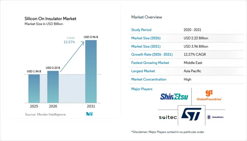
據 Mordor Intelligence 稱,2025 年 SOI(矽晶絕緣體)市場規模為 19.6 億美元,預計在預測期(2026-2031 年)內將以 12.27% 的複合年成長率成長,從 2026 年的 22.2 億美元成長到 2031 億美元。
本報告依SOI平台(FD-SOI、PD-SOI、Power-SOI及其他SOI平台)、晶圓尺寸(200mm以下及201mm以上)、技術(鍵結SOI等)、應用(MEMS、電源、光纖通訊等)、終端用戶產業(家用電子電器、汽車、IT及通訊等)及地區進行細分。市場預測以美元計價。
全球矽晶絕緣體(SOI)市場趨勢與洞察
FD-SOI在5G射頻前端模組中的應用日益廣泛
智慧型手機無線架構整合了更多功率放大器、開關和調諧器,以支援載波聚合。 FD-SOI 技術無需昂貴的基板即可提供必要的線性度和諧波抑制。隨著多頻段旗艦機型的發布,RF-SOI 晶圓出貨量在 2025 年顯著成長。代工廠目前正在生產用於無線應用的 22nm FD-SOI 節點,透過將類比、數位和電源模組整合到單一晶片上,縮小了 PCB 尺寸。即時反向偏壓是 FD-SOI 所遵循的 3GPP Release 18 標準的一項要求,它進一步推動了晶圓需求,並擴大了 SOI(矽晶絕緣體)市場。 FD-SOI 也被應用於大規模 MIMO 無線應用,使其應用範圍擴展到行動電話設備之外。
對高性能、低功耗邊緣人工智慧晶片的需求日益成長
用於汽車、相機和穿戴式裝置的邊緣推理引擎需要達到每秒兆次運算的效能,同時將待機功耗控制在毫瓦級。超薄的FD-SOI封裝可降低漏電流,並支援低至0.4V的低電壓工作,這使得28nm FD-SOI平台在2025年前預計在汽車AI SoC領域得到更廣泛的應用。工程師利用背偏壓來控制-40 度C至125 度C的溫度波動,無需增加保護電壓即可符合安全標準。此方法的標準化將提高晶圓產量、降低成本、加速應用普及,並擴大SOI(矽晶絕緣體)市場。
300mm SOI晶圓產能供需失衡
到2025年,僅有一條300毫米晶圓生產線達到量產能力,擴建計畫延至2027年底。晶圓代工廠面臨的晶圓成本比傳統矽高出20-30%,擠壓了利潤空間,並減緩了向更大直徑晶圓的轉型。一些無廠半導體公司已轉向200毫米節點以確保供應,但這導致生產分散,減緩了成本曲線趨於平緩的進程,並限制了SOI市場的短期成長。由於SOI製程對厚度控制較為嚴格,且300毫米製程氫注入製程需要高額資本投入,主要的傳統矽公司對投資SOI仍持謹慎態度。短期的雙源採購措施只會增加工程成本,且只能提供部分緩解。
細分市場分析
2025年,FD-SOI的銷售額佔比達到54.21%,成為SOI(矽晶絕緣體)市場中最大的佔有率。這主要得益於其在RF收發器、低功耗微控制器和消費性穿戴式裝置的廣泛應用。 OEM廠商選擇該平台的原因在於,它能夠在低於0.5V的電壓下工作,同時確保下一代無線設備所需的增益線性度和雜訊容限。預計從2026年起,功率型SOI(矽晶絕緣體)市場將以13.07%的複合年成長率成長。
在製程技術方面,GlobalFoundries 的 22nm FD-SOI 節點預計到 2025 年底將完成超過 50 款汽車晶片的流片,凸顯了該設計強勁的市場應用動能。意法半導體 (STMicroelectronics) 和三星晶圓代工 (Samsung Foundry) 繼續擴大其模擬和混合訊號產品組合中 FD-SOI 的應用,而英飛凌 (Infineon) 和安森美半導體 (ON Semiconductor) 則將研發重點放在用於 800V 系統的 Power-S 系統上。這種平台的多樣化使得晶圓供應商能夠根據特定應用需求對封裝層和處理層進行微調,從而深化整個 SOI(矽晶絕緣體)產業的價值創造。
2025年,201毫米及以上尺寸的基板將佔總銷售額的68.33%,這反映出一旦產量穩定,由於每片晶圓晶片數量的規模經濟效應,成本可望降低約三分之一。大多數代工廠已在政府補貼計畫的支持下,於歐洲和北美建立了300毫米SOI生產線,進一步鞏固了SOI(矽晶絕緣體)市場的這一細分領域。然而,300毫米的智慧切割需要亞奈米級的厚度均勻性。因此,良率波動會迅速波及數百個晶片,凸顯了此次宣布的產能提升計畫的戰略重要性。
在MEMS麥克風、陀螺儀感測器和整合光電領域,小直徑晶圓仍然具有競爭力,因為這些領域的晶片尺寸遠小於光罩的整體尺寸。 Okmetic和WaferWorks在150毫米和200毫米生產線上保持著盈利的細分市場,利用更短的周期與新創公司合作,迭代產品開發。這種產能為設計人員提供了一個安全閥,以應對300毫米晶圓供應日益緊張的情況,並維持了整個SOI(矽晶絕緣體)市場的韌性。
區域分析
到2025年,亞太地區將佔全球銷售額的46.83%。這主要得益於中國本土晶圓代工廠的快速發展以及日本在精密MEMS製造領域的持續領先地位。台灣和韓國憑藉其尖端的邏輯和儲存技術,進一步深化了市場;而印度的生產連結獎勵計畫計畫則吸引了對封裝和測試環節的投資,從而帶動了晶圓需求的成長。此外,5G基地台和邊緣AI閘道在亞太地區的部署也進一步擴大了FD-SOI和Power-SOI基板的消耗量。
在北美,政府資助的晶圓廠建設計畫與航太和國防領域的長期需求相結合,在這些領域,抗輻射性能至關重要。英特爾、格羅方德和台積電都已開始在美國建造晶圓廠,預計這些晶圓廠在2027年開始量產時將消耗300毫米特種晶圓。歐洲也緊隨其後,在「晶片法案」提供的430億歐元(484億美元)獎勵的支持下,該法案旨在扶持汽車和工業半導體產業。義法半導體、英飛凌和恩智浦已將本地SOI生產能力納入藍圖,以降低供應風險。
中東是最具活力的新興市場,主權財富基金正向專注於光連接模組和人工智慧加速器的半導體製造廠投資數十億美元。阿拉伯聯合大公國和沙烏地阿拉伯的試點生產線計畫利用SOI光電降低資料中心的能耗效率,推動該地區預計13.21%的複合年成長率。儘管南美和非洲的生態系統發展仍處於早期階段,但巴西和南非的試驗計畫表明,隨著政策框架的完善,SOI(矽晶絕緣體)市場未來具有巨大的成長潛力。
其他好處:
- Excel格式的市場預測(ME)表
- 3個月的分析師支持
目錄
第1章:引言
- 研究假設和市場定義
- 調查範圍
第2章:調查方法
第3章執行摘要
第4章 市場狀況
- 市場概覽
- 市場促進因素
- FD-SOI在5G射頻前端模組中的應用日益廣泛
- 對高性能、低功耗邊緣人工智慧晶片的需求日益成長
- 各國政府為保障半導體主權而採取的策略性舉措
- 利用 Power-SOI 提高電動車動力傳動系統的效率
- MEMS感測器在智慧工業4.0應用的廣泛應用
- 利用SOI光電的資料中心光連接模組正快速成長。
- 市場限制因素
- 300mm SOI晶圓產能供需失衡
- 高昂的製造成本與體矽替代技術的比較
- SOI和先進封裝技術整合的複雜性
- 智慧切割過程中智慧財產權所有權和許可的障礙
- 宏觀經濟因素對市場的影響
- 產業價值鏈分析
- 監理情勢
- 技術展望
- 波特五力分析
第5章 市場規模與成長預測
- SOI平台
- 全耗盡型SOI(矽晶絕緣體)(FD-SOI)
- 部分耗盡型SOI(矽晶絕緣體)(PD-SOI)
- 電力 SOI
- 其他類型
- 按晶圓尺寸
- 200毫米或更小
- 201毫米或以上
- 透過技術
- 鍵合 SOI
- 層轉移SOI
- 智慧切割
- 透過使用
- MEMS
- 電源
- 光纖通訊
- 影像感知
- 其他用途
- 按最終用戶行業分類
- 家用電子產品
- 車
- 資訊科技/通訊
- 航太/國防
- 產業
- 其他終端用戶產業
- 按地區
- 北美洲
- 美國
- 加拿大
- 墨西哥
- 南美洲
- 巴西
- 阿根廷
- 其他南美國家
- 歐洲
- 英國
- 德國
- 法國
- 義大利
- 其他歐洲國家
- 亞太地區
- 中國
- 日本
- 印度
- 韓國
- 其他亞太國家
- 中東和非洲
- 中東
- 阿拉伯聯合大公國
- 沙烏地阿拉伯
- 其他中東國家
- 非洲
- 南非
- 埃及
- 其他非洲國家
- 中東
- 北美洲
第6章 競爭情勢
- 市場集中度
- 策略趨勢
- 市佔率分析
- 公司簡介
- Soitec SA
- Shin-Etsu Chemical Co., Ltd.
- GlobalWafers Co., Ltd.
- GlobalFoundries Inc.
- STMicroelectronics NV
- NXP Semiconductors NV
- Samsung Electronics Co., Ltd.
- Taiwan Semiconductor Manufacturing Company Limited
- Intel Corporation
- Siltronic AG
- SUMCO Corporation
- Okmetic Oyj
- Wafer Works Corporation
- NTT Advanced Technology Corporation
- China Silicon Corporation
- Skyworks Solutions, Inc.
- Infineon Technologies AG
- Murata Manufacturing Co., Ltd.
- Advanced Micro Devices, Inc.
- Analog Devices, Inc.
第7章 市場機會與未來展望
According to Mordor Intelligence, the silicon-on-insulator market size was valued at USD 1.96 billion in 2025 and is estimated to grow from USD 2.22 billion in 2026 to USD 3.96 billion by 2031, at a CAGR of 12.27% during the forecast period (2026-2031).
This report is Segmented by SOI Platform (FD-SOI, PD-SOI, Power-SOI, and Other SOI Platforms), Wafer Size (≤200 Mm, and ≥201 Mm), Technology (Bonding SOI, and More), Application (MEMS, Power Supplies, Optical Communication, and More), End-User Vertical (Consumer Electronics, Automotive, IT and Telecommunication, and More), and Geography. The Market Forecasts are Provided in Terms of Value (USD).
Global Silicon On Insulator Market Trends and Insights
Expanding Adoption of FD-SOI in 5G RF Front-End Modules
Smartphone radio architectures integrate more power amplifiers, switches, and tuners to support carrier aggregation, with FD-SOI providing required linearity and harmonic suppression without costlier substrates. RF-SOI wafer shipments grew significantly in 2025 as multi-band flagships launched. Foundries now produce 22 nm FD-SOI nodes for radio applications, combining analog, digital, and power blocks on a single die to reduce PCB footprints. 3GPP Release 18 standards, met by FD-SOI through real-time back-biasing, further drive wafer demand, boosting the silicon-on-insulator market. FD-SOI is also being adopted for massive-MIMO radios, expanding growth beyond handsets.
Growing Demand for High-Performance, Low-Power Edge AI Chips
Edge inference engines in vehicles, cameras, and wearables must meet milliwatt standby budgets while delivering tera-operations-per-second performance. FD-SOI's ultra-thin body reduces leakage and supports operation down to 0.4 V, driving automotive AI SoCs to adopt 28 nm FD-SOI platforms in 2025. Engineers use back-bias to manage temperature swings from -40 °C to 125 °C, meeting safety mandates without adding guard-band voltage. Standardizing this approach increases wafer volume, lowers costs, and boosts adoption, expanding the silicon-on-insulator market.
Supply-Demand Imbalance in 300 mm SOI Wafer Capacity
By 2025, only one high-volume 300 mm line reached scale, with expansions delayed until late 2027. Foundries face wafer costs 20%-30% higher than those for bulk silicon, squeezing margins and slowing migration to larger diameters. Some fabless customers shifted to 200 mm nodes to secure supply, but this diluted volumes and delayed cost curves, limiting near-term SOI market growth. Bulk-silicon giants remain cautious about SOI capex due to tighter thickness control and the higher capital intensity required for 300 mm hydrogen-implantation steps. Short-term dual-sourcing remedies raise engineering overhead, providing only partial relief.
Other drivers and restraints analyzed in the detailed report include:
- Governments' Strategic Semiconductor Sovereignty Initiatives
- Electric-Vehicle Powertrain Efficiency Improvements Using Power-SOI
- High Fabrication Cost Versus Bulk Silicon Alternatives
For complete list of drivers and restraints, kindly check the Table Of Contents.
Segment Analysis
The 54.21% revenue share held by FD-SOI in 2025 was the largest slice of the silicon-on-insulator market, buoyed by widespread deployment in RF transceivers, low-power microcontrollers, and consumer wearables. OEMs selected the platform for its ability to operate below 0.5 V while still delivering the gain linearity and noise margins demanded by next-generation radios. The silicon-on-insulator market size for Power-SOI is projected to grow at a 13.07% CAGR between 2026 and
At the process-technology level, GlobalFoundries' 22 nm FD-SOI node recorded more than 50 automotive tape-outs by year-end 2025, confirming robust design-win momentum. STMicroelectronics and Samsung Foundry continue to proliferate FD-SOI across analog and mixed-signal catalogs, whereas Infineon and ON Semiconductor channel R&D toward Power-SOI for 800 V drive trains. This platform bifurcation enables wafer suppliers to fine-tune box and handle layers for application-specific needs, deepening value capture across the silicon-on-insulator industry.
Substrates measuring 201 mm or more captured 68.33% of 2025 revenue, reflecting die-per-wafer leverage that cuts costs by roughly one-third once volume reaches steady state. Most foundries are positioning 300 mm SOI lines in Europe and North America under government-backed subsidy programs, further anchoring this segment of the silicon-on-insulator market. However, Smart Cut at 300 mm demands sub-nanometer thickness uniformity; yield excursions therefore ripple quickly across hundreds of dies, underscoring the strategic importance of announced capacity increases.
Smaller diameters retain vitality in MEMS microphones, gyro sensors, and integrated photonics, where die footprints cap out far below a full reticle. Okmetic and Wafer Works maintain profitable niches in 150 mm and 200 mm runs, using faster cycle times to iterate alongside start-ups. Such capacity provides a relief valve, as designers hedge against the tight supply of 300 mm blanks, preserving resilience across the broader silicon-on-insulator market.
Geography Analysis
Asia-Pacific commanded 46.83% of global revenue in 2025, anchored by China's indigenous foundry surge and Japan's enduring edge in precision MEMS fabrication. Taiwan and South Korea add depth through leading-edge logic and memory, while India's Production-Linked Incentive scheme is drawing assembly and test investments that will back-propagate wafer demand. Regional build-outs in 5G base stations and edge AI gateways further multiply consumption of FD-SOI and Power-SOI substrates.
North America combines sovereign-funded fab projects with long-standing aerospace and defense applications that value SOI for radiation hardness. Intel, GlobalFoundries, and TSMC have each broken ground on U.S. facilities slated to consume 300-mm specialty wafers when ramping begins in 2027. Europe follows closely, supported by EUR 43 billion (USD 48.4 billion) in Chips Act incentives that target automotive and industrial semiconductors. STMicroelectronics, Infineon, and NXP are already integrating localized SOI capacity into their roadmap to de-risk supply.
The Middle East represents the most dynamic frontier, with sovereign wealth funds allocating multibillion-dollar capital pools to semiconductor fabs focused on optical interconnects and AI accelerators. Pilot lines in the United Arab Emirates and Saudi Arabia plan to leverage SOI photonics to lower data-center energy intensity, reinforcing a 13.21% CAGR outlook for the region. South America and Africa are early in ecosystem development; nonetheless, pilot programs in Brazil and South Africa signal future upside for the silicon on insulator market as policy frameworks mature.
- Soitec SA
- Shin-Etsu Chemical Co., Ltd.
- GlobalWafers Co., Ltd.
- GlobalFoundries Inc.
- STMicroelectronics N.V.
- NXP Semiconductors N.V.
- Samsung Electronics Co., Ltd.
- Taiwan Semiconductor Manufacturing Company Limited
- Intel Corporation
- Siltronic AG
- SUMCO Corporation
- Okmetic Oyj
- Wafer Works Corporation
- NTT Advanced Technology Corporation
- China Silicon Corporation
- Skyworks Solutions, Inc.
- Infineon Technologies AG
- Murata Manufacturing Co., Ltd.
- Advanced Micro Devices, Inc.
- Analog Devices, Inc.
Additional Benefits:
- The market estimate (ME) sheet in Excel format
- 3 months of analyst support
TABLE OF CONTENTS
1 INTRODUCTION
- 1.1 Study Assumptions and Market Definition
- 1.2 Scope of the Study
2 RESEARCH METHODOLOGY
3 EXECUTIVE SUMMARY
4 MARKET LANDSCAPE
- 4.1 Market Overview
- 4.2 Market Drivers
- 4.2.1 Expanding Adoption of FD-SOI in 5G RF Front-End Modules
- 4.2.2 Growing Demand for High-Performance, Low-Power Edge AI Chips
- 4.2.3 Governments' Strategic Semiconductor Sovereignty Initiatives
- 4.2.4 Electric Vehicle Powertrain Efficiency Improvements Using Power-SOI
- 4.2.5 Rising Use of MEMS Sensors in Smart Industry 4.0 Applications
- 4.2.6 Surge in Optical Interconnects for Data Centers Leveraging SOI Photonics
- 4.3 Market Restraints
- 4.3.1 Supply-Demand Imbalance in 300 mm SOI Wafer Capacity
- 4.3.2 High Fabrication Cost Versus Bulk Silicon Alternatives
- 4.3.3 Complexity of Integrating SOI with Advanced Packaging Technologies
- 4.3.4 IP Ownership and Licensing Barriers in Smart Cut Process
- 4.4 Impact of Macroeconomic Factors on the Market
- 4.5 Industry Value Chain Analysis
- 4.6 Regulatory Landscape
- 4.7 Technological Outlook
- 4.8 Porter's Five Forces Analysis
- 4.8.1 Bargaining Power of Suppliers
- 4.8.2 Bargaining Power of Buyers
- 4.8.3 Threat of New Entrants
- 4.8.4 Threat of Substitutes
- 4.8.5 Intensity of Competitive Rivalry
5 MARKET SIZE AND GROWTH FORECASTS (VALUE)
- 5.1 By SOI Platform
- 5.1.1 Fully Depleted Silicon on Insulator (FD-SOI)
- 5.1.2 Partially Depleted Silicon on Insulator (PD-SOI)
- 5.1.3 Power-SOI
- 5.1.4 Other Types
- 5.2 By Wafer Size
- 5.2.1 Less Than or Equal To 200 mm
- 5.2.2 201 mm and Above
- 5.3 By Technology
- 5.3.1 Bonding SOI
- 5.3.2 Layer Transfer SOI
- 5.3.3 Smart Cut
- 5.4 By Application
- 5.4.1 MEMS
- 5.4.2 Power Supplies
- 5.4.3 Optical Communication
- 5.4.4 Image Sensing
- 5.4.5 Other Applications
- 5.5 By End-User Vertical
- 5.5.1 Consumer Electronics
- 5.5.2 Automotive
- 5.5.3 IT and Telecommunication
- 5.5.4 Aerospace and Defense
- 5.5.5 Industrial
- 5.5.6 Other End User Verticals
- 5.6 By Geography
- 5.6.1 North America
- 5.6.1.1 United States
- 5.6.1.2 Canada
- 5.6.1.3 Mexico
- 5.6.2 South America
- 5.6.2.1 Brazil
- 5.6.2.2 Argentina
- 5.6.2.3 Rest of South America
- 5.6.3 Europe
- 5.6.3.1 United Kingdom
- 5.6.3.2 Germany
- 5.6.3.3 France
- 5.6.3.4 Italy
- 5.6.3.5 Rest of Europe
- 5.6.4 Asia-Pacific
- 5.6.4.1 China
- 5.6.4.2 Japan
- 5.6.4.3 India
- 5.6.4.4 South Korea
- 5.6.4.5 Rest of Asia-Pacific
- 5.6.5 Middle East and Africa
- 5.6.5.1 Middle East
- 5.6.5.1.1 United Arab Emirates
- 5.6.5.1.2 Saudi Arabia
- 5.6.5.1.3 Rest of Middle East
- 5.6.5.2 Africa
- 5.6.5.2.1 South Africa
- 5.6.5.2.2 Egypt
- 5.6.5.2.3 Rest of Africa
- 5.6.5.1 Middle East
- 5.6.1 North America
6 COMPETITIVE LANDSCAPE
- 6.1 Market Concentration
- 6.2 Strategic Moves
- 6.3 Market Share Analysis
- 6.4 Company Profiles (includes Global Level Overview, Market Level Overview, Core Segments, Financials as available, Strategic Information, Market Rank/Share, Products and Services, Recent Developments)
- 6.4.1 Soitec SA
- 6.4.2 Shin-Etsu Chemical Co., Ltd.
- 6.4.3 GlobalWafers Co., Ltd.
- 6.4.4 GlobalFoundries Inc.
- 6.4.5 STMicroelectronics N.V.
- 6.4.6 NXP Semiconductors N.V.
- 6.4.7 Samsung Electronics Co., Ltd.
- 6.4.8 Taiwan Semiconductor Manufacturing Company Limited
- 6.4.9 Intel Corporation
- 6.4.10 Siltronic AG
- 6.4.11 SUMCO Corporation
- 6.4.12 Okmetic Oyj
- 6.4.13 Wafer Works Corporation
- 6.4.14 NTT Advanced Technology Corporation
- 6.4.15 China Silicon Corporation
- 6.4.16 Skyworks Solutions, Inc.
- 6.4.17 Infineon Technologies AG
- 6.4.18 Murata Manufacturing Co., Ltd.
- 6.4.19 Advanced Micro Devices, Inc.
- 6.4.20 Analog Devices, Inc.
7 MARKET OPPORTUNITIES AND FUTURE OUTLOOK
- 7.1 White-Space and Unmet-Need Assessment
 絕緣體上矽(SOI)市場報告:按晶圓尺寸、晶圓類型、技術、產品、應用和地區分類(2026-2034 年)
 SOI(絕緣薄膜矽)市場:依產品類型、晶圓尺寸、晶圓類型、技術、厚度和應用分類-2026-2032年全球市場預測
 SOI矽晶片:市佔率分析、產業趨勢與統計、成長預測(2026-2031年)
 絕緣體上矽 (SOI) 市場分析及至 2035 年預測:按類型、產品類型、技術、組件、應用、材料類型、裝置、製程和最終用戶分類
 絕緣體上矽(SOI)全球市場規模、佔有率、趨勢和成長分析報告(2026-2034)
 2026年全球SOI(絕緣體上矽)市場報告
 絕緣體上矽 (SOI) 市場規模、佔有率和成長分析(按晶圓類型、晶圓尺寸、技術、應用、最終用戶和地區分類)—產業預測:2026-2033 年
 FD-SOI(全耗盡型SOI)技術:全球市場佔有率和排名、總收入和需求預測(2025-2031年)
 全球厚膜腔SOI晶圓市場(2025年)
 2032 年 SOI(絕緣體上矽)市場預測:按產品、晶圓類型、厚度、晶圓尺寸、技術、最終用戶和地區進行的全球分析