


 |
市場調查報告書
商品編碼
2043993
SOI矽晶片:市佔率分析、產業趨勢與統計、成長預測(2026-2031年)SOI Silicon Wafer - Market Share Analysis, Industry Trends & Statistics, Growth Forecasts (2026 - 2031) |
||||||
※ 本網頁內容可能與最新版本有所差異。詳細情況請與我們聯繫。
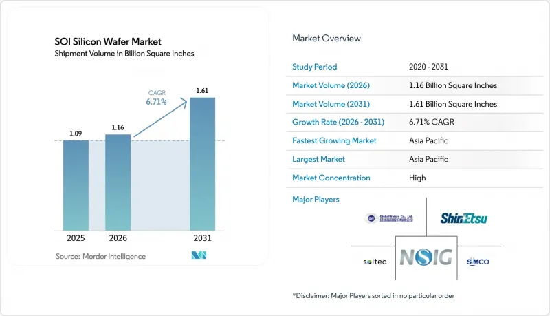
2025 年 SOI 矽晶片市場規模為 10.9 億平方英寸,預計到 2031 年將達到 11.6 億平方英寸,而 2026 年為 11.6 億平方英寸,預測期(2026-2031 年)複合年成長率為 6.71%。
SOI技術的成長主要得益於其介電隔離和背偏壓柔軟性等應用,例如5G射頻前端模組、汽車電源管理IC和矽光電互連等。然而,300mm基板的產能限制、成本仍比體矽高出2-3倍,以及Soytec「智慧切割」製程相關的智慧財產權壁壘等因素,都阻礙了SOI技術的成長。儘管如此,這些因素並不會阻礙SOI技術的普及,因為目前代工廠的製程藍圖優先考慮的是28nm以下製程的全耗盡SOI節點,而非體矽CMOS。雖然亞太地區的SOI出貨量主導,但由於美國和歐洲的政策主導產能提升,該地區的風險模式正在改變。因此,元件製造商正在調整其SOI矽晶圓市場的長期供應策略,以平衡性能提升、晶圓供應和單位成本效益。
全球SOI矽晶圓市場趨勢與洞察
FD-SOI在5G射頻前端模組中的快速普及
對於5G和早期6G智慧型手機的高頻前端模組,為了在毫米波頻段實現線性度和插入損耗目標(這些目標難以透過體矽CMOS製程實現),越來越依賴RF-SOI和FD-SOI基板。 GlobalFoundries的9SW平台將開關和低雜訊擴大機整合在300mm RF-SOI基板上,使行動電話製造商能夠在滿足嚴格的功耗預算的同時,將基板面積減少30%。 Tower Semiconductor已將類似技術擴展到Wi-Fi 7,並與Broadcom合作,在6GHz頻段實現了低於0.4dB的插入損耗。 2026年初,蘋果iPhone 17採用了高通公司基於22FDX FD-SOI製程製造的QTM565天線模組,展示了其在量產上的應用。 VeriSilicon已出貨超過1億顆FD-SOI互連晶片,支援了SOI矽晶圓市場主流化的趨勢,並擴大了其潛在市場。隨著行動電話製造商向 6G 整合邁進,由於晶片面積增大和晶圓價格上漲,基板供應商的需求增加,並從中受益。
擴大SOI在汽車ADAS和電源管理IC中的整合
汽車製造商正將電池管理IC和成像雷達收發器遷移到SOI封裝,以符合ISO 26262功能安全標準並避免48V電氣系統中的閂鎖效應。 Soytech的Power-SOI系列支援200V工作電壓,並透過使電池監控IC無需昂貴的隔離級即可監控30節電池串,從而降低15%的組件成本。預計到2030年,汽車雷達銷售額將達到220億美元,而22nm FD-SOI製程可實現超過350GHz的運作頻率,滿足4D雷達的要求。意法半導體(STMicroelectronics)和恩智浦半導體(NXP)已獲得300mm Power-SOI生產線的認證,顯示其產品已準備好量產。隨著電動車產量的成長,基於SOI的分離式功率處理器和混合訊號處理器正成為標準選擇,從而提升了SOI矽晶圓市場的長期成長前景。
300mm SOI晶圓生產全球產能受限
全球範圍內,300mm SOI晶圓的年產量不足300萬片,僅佔300mm體矽總供應量的不到2%。 Soytech位於伯南德和新加坡的工廠年產量約200萬片,而信越化學和SUMCO的年產量僅50萬片。 Ocmetic的2026年擴建計畫旨在滿足200mm的需求,而非300mm,產能缺口將持續到Global Wafers位於美國和義大利的工廠於2027年下半年投入量產為止。這種供不應求迫使代工廠簽訂多季度契約,基板價格正以個位數的速度逐年上漲,SOI矽晶圓市場的短期成長可能在新生產線運作前趨於平穩。
細分市場分析
預計到2025年,300mm規格的SOI矽晶圓產量將佔總產量的47.74%,並在2031年之前以7.17%的複合年成長率持續成長,成為預測期內SOI矽晶圓市場規模的主要驅動力。 GlobalFoundries、STMicroelectronics和Tower Semiconductor等代工廠正在將RF-SOI和FD-SOI製程標準化應用於300mm設備,以降低晶圓成本並重複利用已針對低缺陷密度最佳化的成熟工具集。隨著新型5G、Wi-Fi 7和汽車雷達設計從200mm製程轉向300mm工藝,基板需求正在加速成長,進一步推動了SOI矽晶圓市場的發展。
然而,汽車級功率SOI技術的發展仍依賴200mm生產線。這是因為這些晶圓廠的設備已經折舊免稅額,並且已經獲得了支援較長產品生命週期的認證。供應商可能會繼續維持混合生產模式,直到全球需求足夠強勁,足以支撐每條300mm智慧切割生產線1億美元的投資。小於150mm的晶圓在抗輻射的航太電子產品領域仍具有重要的市場地位,因為這些領域的認證週期超過10年。因此,晶圓直徑的模式仍將保持兩極化,但預計到2031年,SOI矽晶圓市場的收入中心將繼續轉移到300mm基板。
《SOI矽晶圓市場報告》以晶圓直徑(150毫米及以下、200毫米、300毫米)、半導體裝置類型(邏輯裝置、記憶體、類比元件、分立元件及其他元件類型)、最終用戶(消費性電子、工業、通訊、汽車及其他最終用戶)及地區進行細分。市場預測以體積(平方英吋)為單位。
區域分析
預計到2025年,亞太地區將佔全球出貨量的83.22%,並將在2031年之前保持領先地位,年複合成長率(CAGR)為7.22%。台灣晶圓代工廠支撐著區域需求,而日本的信越化學工業株式會社和SUMCO則負責本地基板供應。中國正在上海森貴擴大其200mm SOI晶圓的國內產能,並正在研究300mm晶圓的產能,以減少對進口的依賴,從而進一步擴大區域SOI晶圓市場。
在北美,隨著GlobalWafers位於密蘇裡州和德克薩斯州的運作於2027年投產,預計市場成長將加速。這將使GlobalWafers能夠為汽車、國防和電信等優先考慮穩定採購的產業客戶提供本土供應。歐洲的發展路徑也與此類似。意法半導體(STMicroelectronics)位於克羅爾(Kroll)的300毫米FD-SOI工廠以及GlobalWafers位於諾瓦拉(Novara)的工廠(由歐盟晶片法案資助)旨在降低供應鏈風險,並滿足區域原始設備製造商(OEM)對符合大地測量原點要求的需求。這些發展共同推動全球SOI矽晶圓市場擺脫目前以亞洲為中心的格局,實現多元化。
在南美洲、中東和非洲,由於缺乏代工基礎設施,供應非常有限。以色列的Tower Semiconductor公司透過其本地晶圓廠向全球供應射頻SOI模組,並在中東地區保持重要的市場佔有率。隨著各國政府將補貼與國內生產能力掛鉤,預計區域多元化趨勢將持續,地緣政治風險對整個SOI矽晶圓市場的影響可能會逐步降低。
其他好處
- Excel格式的市場預測(ME)表
- 3個月的分析師支持
目錄
第1章:引言
- 研究假設和市場定義
- 調查範圍
第2章:調查方法
第3章執行摘要
第4章 市場狀況
- 市場概覽
- 產業價值鏈分析
- 技術展望
- 宏觀經濟因素對市場的影響
- 波特五力分析
- 供應商的議價能力
- 買方的議價能力
- 新進入者的威脅
- 替代品的威脅
- 競爭公司之間的競爭
- 市場促進因素
- FD-SOI在5G射頻前端模組中的快速普及
- SOI技術在汽車ADAS和電源管理IC的應用正在取得進展。
- 亞洲和歐洲政府對國內300mm SOI製造的支持措施
- 超大規模資料中心對矽光電的需求激增
- 基於SOI基板的新興神經形態和量子運算控制晶片
- 向混合訊號物聯網設備過渡,需要超低漏電流的SOI節點
- 市場限制因素
- 全球300毫米SOI晶圓產能短缺
- 與塊狀矽基基板相比,成本溢價更高
- 與 SmartCut 和 Eltran 製程相關的智慧財產權集中
- 先進FD-SOI製程中的晶圓邊緣空洞缺陷會導致良率下降。
第5章 市場規模與成長預測
- 依晶圓直徑
- 最大 150 毫米
- 200mm
- 300mm
- 依半導體裝置類型
- 邏輯
- 記憶
- 模擬
- 離散的
- 其他半導體裝置類型
- 最終用戶
- 家用電器
- 手機和智慧型手機
- PC和伺服器
- 工業的
- 溝通
- 車
- 其他終端用戶應用程式
- 家用電器
- 按地區
- 北美洲
- 美國
- 加拿大
- 墨西哥
- 歐洲
- 德國
- 英國
- 法國
- 其他歐洲國家
- 亞太地區
- 中國
- 日本
- 印度
- 韓國
- 台灣
- 亞太其他地區
- 南美洲
- 中東和非洲
- 北美洲
第6章 競爭情勢
- 市場集中度
- 策略趨勢
- 市佔率分析
- 公司簡介
- Soitec SA
- Shin-Etsu Chemical Co., Ltd.
- GlobalWafers Co., Ltd.
- SUMCO Corporation
- SK Siltron Co., Ltd.
- Okmetic Oy
- Shanghai Simgui Technology Co., Ltd.
- Wafer Works Corporation
- Siltronic AG
- GlobalFoundries Inc.
- Taiwan Semiconductor Manufacturing Company Limited
- Samsung Electronics Co., Ltd.
- STMicroelectronics NV
- NXP Semiconductors NV
- Tower Semiconductor Ltd.
- United Microelectronics Corporation
- ON Semiconductor Corporation
- IQE plc
- Semiconductor Manufacturing International Corporation
- Advanced Micro Foundry Pte. Ltd.
第7章 市場機會與未來展望
The SOI silicon wafer market size was 1.09 billion square inches in 2025 and is estimated to grow from 1.16 billion square inches in 2026 to reach 1.61 billion square inches by 2031, at a CAGR of 6.71% during the forecast period (2026-2031).
Momentum stems from 5G radio-frequency front-end modules, automotive power-management ICs, and silicon-photonics interconnects that demand the dielectric isolation and back-bias flexibility SOI provides. Capacity constraints on 300 mm substrates, a persistent 2-to-3-times cost premium over bulk silicon, and the intellectual-property moat around Soitec's Smart Cut process temper growth but do not derail adoption, because foundry roadmaps now favor fully depleted SOI nodes over bulk CMOS at 28 nm and below. Asia-Pacific dominates shipments, yet policy-driven capacity additions in the United States and Europe are reshaping geographic risk. Device makers therefore juggle performance gains against wafer availability and unit economics as they plan long-term supply strategies for the SOI silicon wafer market.
Global SOI Silicon Wafer Market Trends and Insights
Rapid Adoption of FD-SOI for 5G RF Front-End Modules
Radio-frequency front-end modules for 5G and early 6G smartphones increasingly rely on RF-SOI and FD-SOI substrates to satisfy linearity and insertion-loss targets at millimeter-wave frequencies, where bulk CMOS struggles. GlobalFoundries' 9SW platform integrates switches and low-noise amplifiers on 300 mm RF-SOI, enabling handset makers to shrink board area by 30% while meeting stringent power budgets. Tower Semiconductor extended similar technology to Wi-Fi 7, partnering with Broadcom to achieve sub-0.4 dB insertion loss at 6 GHz. High-volume validation arrived when Apple's iPhone 17 used Qualcomm's QTM565 antenna module fabricated on 22FDX FD-SOI in early 2026. VeriSilicon has already shipped more than 100 million FD-SOI connectivity chips, underscoring a mainstream shift that widens the addressable SOI silicon wafer market. As handset OEMs pursue 6G integration, substrate suppliers benefit from richer die-area requirements and premium wafer pricing.
Increasing Integration of SOI in Automotive ADAS and Power-Management ICs
Vehicle makers have migrated battery-management ICs and imaging-radar transceivers to SOI to meet ISO 26262 functional-safety standards and to avoid latch-up in 48-volt electrical systems. Soitec's Power-SOI family supports 200-volt operation, allowing battery-monitor ICs to supervise 30-cell strings without costly isolation stages, cutting bill-of-materials cost by 15%. Automotive radar revenue is on track to reach USD 22 billion by 2030, and 22 nm FD-SOI processes deliver transit frequencies above 350 GHz, aligning with 4D radar requirements. STMicroelectronics and NXP have qualified 300 mm Power-SOI lines, signaling volume readiness. As electric-vehicle production climbs, discrete power and mixed-signal processors built on SOI are becoming default choices, lifting the long-term growth outlook for the SOI silicon wafer market.
Limited Global Capacity for 300 mm SOI Wafer Production
Worldwide, 300 mm SOI output remains below 3 million wafers per year, less than 2% of the total 300 mm bulk-silicon supply. Soitec's Bernin and Singapore plants deliver roughly 2 million wafers, while Shin-Etsu and SUMCO contribute only 0.5 million. Okmetic's 2026 expansion addressed 200 mm demand rather than 300 mm, leaving a capacity gap until GlobalWafers' U.S. and Italian plants reach volume in late 2027. Scarcity forces foundries into multi-quarter commitments, raises substrate prices by single-digit percentages each year, and threatens to cap near-term growth for the SOI silicon wafer market until new lines come online.
Other drivers and restraints analyzed in the detailed report include:
- Government Incentives for Domestic 300 mm SOI Fabs in Asia and Europe
- Demand Surge from Silicon Photonics in Hyperscale Data Centers
- Higher Cost Premium Over Bulk Silicon Substrates
For complete list of drivers and restraints, kindly check the Table Of Contents.
Segment Analysis
The 300 mm segment accounted for 47.74% of 2025 volume and is projected to expand at a 7.17% CAGR to 2031, making it the primary volume driver for the SOI silicon wafer market size over the forecast horizon. Foundries including GlobalFoundries, STMicroelectronics, and Tower Semiconductor have standardized RF-SOI and FD-SOI processes on 300 mm equipment to capture die-cost savings and to reuse mature tool sets already optimized for low-defect density. As new 5G, Wi-Fi 7, and automotive radar designs transit from 200 mm to 300 mm flows, substrate demand accelerates, further lifting the SOI silicon wafer market.
Advances in automotive Power-SOI, however, still rely on 200 mm lines because those fabs are fully depreciated and already qualified for long model-year lifecycles. Until global demand justifies the USD 100 million investment per Smart Cut line at 300 mm, suppliers will keep a hybrid footprint. Sub-150 mm formats retain niche relevance in radiation-hardened aerospace electronics, where qualification cycles run a decade or longer. Consequently, the wafer-diameter mix will remain bifurcated, but the revenue center of the SOI silicon wafer market will continue to pivot toward 300 mm substrates through 2031.
The SOI Silicon Wafer Market Report is Segmented by Wafer Diameter (Up To 150mm, 200mm, and 300mm), Semiconductor Device Type (Logic, Memory, Analog, Discrete, and Other Device Types), End-User (Consumer Electronics, Industrial, Telecommunications, Automotive, and Other End-Users), and Geography. The Market Forecasts are Provided in Terms of Volume (Square Inches).
Geography Analysis
Asia-Pacific held 83.22% of 2025 shipments and is set to maintain volume leadership with a 7.22% CAGR through 2031. Taiwan's foundries anchor regional demand, while Japan's Shin-Etsu and SUMCO provide local substrate supply. China is ramping domestic 200 mm SOI at Shanghai Simgui and researching 300 mm capacity to reduce reliance on imports, further expanding the regional SOI silicon wafer market.
North America is poised for accelerated growth once GlobalWafers' Missouri and Texas plants come online in 2027, offering a domestic supply to automotive, defense, and telecom customers that prize secure sourcing. Europe follows a parallel path; STMicroelectronics' 300 mm FD-SOI fab in Crolles and GlobalWafers' Novara plant, supported by EU Chips Act funding, aim to mitigate supply-chain risk and meet the needs of regional OEMs that require origin compliance. Together, these developments diversify the global SOI silicon wafer market away from its current Asia-heavy base.
South America and the Middle East, and Africa account for marginal volumes, constrained by limited foundry infrastructure. Nonetheless, Israel's Tower Semiconductor does supply global RF-SOI modules from its local fabs, maintaining a modest Middle Eastern footprint. Regional diversification trends will continue as governments tie subsidies to domestic capacity, incrementally lowering geopolitical risk across the SOI silicon wafer market.
- Soitec SA
- Shin-Etsu Chemical Co., Ltd.
- GlobalWafers Co., Ltd.
- SUMCO Corporation
- SK Siltron Co., Ltd.
- Okmetic Oy
- Shanghai Simgui Technology Co., Ltd.
- Wafer Works Corporation
- Siltronic AG
- GlobalFoundries Inc.
- Taiwan Semiconductor Manufacturing Company Limited
- Samsung Electronics Co., Ltd.
- STMicroelectronics N.V.
- NXP Semiconductors N.V.
- Tower Semiconductor Ltd.
- United Microelectronics Corporation
- ON Semiconductor Corporation
- IQE plc
- Semiconductor Manufacturing International Corporation
- Advanced Micro Foundry Pte. Ltd.
Additional Benefits:
- The market estimate (ME) sheet in Excel format
- 3 months of analyst support
TABLE OF CONTENTS
1 INTRODUCTION
- 1.1 Study Assumptions and Market Definition
- 1.2 Scope of the Study
2 RESEARCH METHODOLOGY
3 EXECUTIVE SUMMARY
4 MARKET LANDSCAPE
- 4.1 Market Overview
- 4.2 Industry Value-Chain Analysis
- 4.3 Technological Outlook
- 4.4 Impact of Macroeconomic Factors on the Market
- 4.5 Porter's Five Forces Analysis
- 4.5.1 Bargaining Power of Suppliers
- 4.5.2 Bargaining Power of Buyers
- 4.5.3 Threat of New Entrants
- 4.5.4 Threat of Substitutes
- 4.5.5 Intensity of Competitive Rivalry
- 4.6 Market Drivers
- 4.6.1 Rapid Adoption of FD-SOI for 5G RF Front-end Modules
- 4.6.2 Increasing Integration of SOI in Automotive ADAS and Power Management ICs
- 4.6.3 Government Incentives for Domestic 300 mm SOI Fabs in Asia and Europe
- 4.6.4 Demand Surge from Silicon Photonics in Hyperscale Data Centers
- 4.6.5 Emerging Neuromorphic and Quantum Computing Control Chips on SOI Substrates
- 4.6.6 Transition Toward Mixed-Signal IoT Devices Requiring Ultra-Low-Leakage SOI Nodes
- 4.7 Market Restraints
- 4.7.1 Limited Global Capacity for 300 mm SOI Wafer Production
- 4.7.2 Higher Cost Premium Over Bulk Silicon Substrates
- 4.7.3 Intellectual-Property Concentration Around Smart Cut and Eltran Processes
- 4.7.4 Wafer Edge-Void Defects Causing Yield Losses in Advanced FD-SOI Nodes
5 MARKET SIZE AND GROWTH FORECASTS (VOLUME)
- 5.1 By Wafer Diameter
- 5.1.1 Up to 150 mm
- 5.1.2 200 mm
- 5.1.3 300 mm
- 5.2 By Semiconductor Device Type
- 5.2.1 Logic
- 5.2.2 Memory
- 5.2.3 Analog
- 5.2.4 Discrete
- 5.2.5 Other Semiconductor Device Types
- 5.3 By End-user
- 5.3.1 Consumer Electronics
- 5.3.1.1 Mobile and Smartphones
- 5.3.1.2 PCs and Servers
- 5.3.2 Industrial
- 5.3.3 Telecommunications
- 5.3.4 Automotive
- 5.3.5 Other End-user Applications
- 5.3.1 Consumer Electronics
- 5.4 By Geography
- 5.4.1 North America
- 5.4.1.1 United States
- 5.4.1.2 Canada
- 5.4.1.3 Mexico
- 5.4.2 Europe
- 5.4.2.1 Germany
- 5.4.2.2 United Kingdom
- 5.4.2.3 France
- 5.4.2.4 Rest of Europe
- 5.4.3 Asia-Pacific
- 5.4.3.1 China
- 5.4.3.2 Japan
- 5.4.3.3 India
- 5.4.3.4 South Korea
- 5.4.3.5 Taiwan
- 5.4.3.6 Rest of Asia-Pacific
- 5.4.4 South America
- 5.4.5 Middle East and Africa
- 5.4.1 North America
6 COMPETITIVE LANDSCAPE
- 6.1 Market Concentration
- 6.2 Strategic Moves
- 6.3 Market Share Analysis
- 6.4 Company Profiles (includes Global Level Overview, Market Level Overview, Core Segments, Financials as available, Strategic Information, Market Rank/Share, Products and Services, Recent Developments)
- 6.4.1 Soitec SA
- 6.4.2 Shin-Etsu Chemical Co., Ltd.
- 6.4.3 GlobalWafers Co., Ltd.
- 6.4.4 SUMCO Corporation
- 6.4.5 SK Siltron Co., Ltd.
- 6.4.6 Okmetic Oy
- 6.4.7 Shanghai Simgui Technology Co., Ltd.
- 6.4.8 Wafer Works Corporation
- 6.4.9 Siltronic AG
- 6.4.10 GlobalFoundries Inc.
- 6.4.11 Taiwan Semiconductor Manufacturing Company Limited
- 6.4.12 Samsung Electronics Co., Ltd.
- 6.4.13 STMicroelectronics N.V.
- 6.4.14 NXP Semiconductors N.V.
- 6.4.15 Tower Semiconductor Ltd.
- 6.4.16 United Microelectronics Corporation
- 6.4.17 ON Semiconductor Corporation
- 6.4.18 IQE plc
- 6.4.19 Semiconductor Manufacturing International Corporation
- 6.4.20 Advanced Micro Foundry Pte. Ltd.
7 MARKET OPPORTUNITIES AND FUTURE OUTLOOK
- 7.1 White-space and Unmet-need Assessment
 絕緣體上矽市場-2026-2032年全球市場預測
 絕緣體上矽 (SOI) 市場預測至 2034 年—按晶圓類型、晶圓尺寸、技術、節點尺寸、應用、最終用戶和地區分類的全球分析
 絕緣體上矽 (SOI) 市場:按材料、外形尺寸、技術、應用、最終用途、國家和地區分類 - 全球行業分析、市場規模、市場佔有率和預測 (2026–2033)
 SOI(矽晶絕緣體):市場佔有率分析、產業趨勢與統計、成長預測(2026-2031)
 絕緣體上矽(SOI)市場報告:按晶圓尺寸、晶圓類型、技術、產品、應用和地區分類(2026-2034 年)
 絕緣體上矽 (SOI) 市場分析及至 2035 年預測:按類型、產品類型、技術、組件、應用、材料類型、裝置、製程和最終用戶分類
 絕緣體上矽(SOI)全球市場規模、佔有率、趨勢和成長分析報告(2026-2034)
 2026年全球SOI(絕緣體上矽)市場報告
 絕緣體上矽 (SOI) 市場規模、佔有率和成長分析(按晶圓類型、晶圓尺寸、技術、應用、最終用戶和地區分類)—產業預測:2026-2033 年
 FD-SOI(全耗盡型SOI)技術:全球市場佔有率和排名、總收入和需求預測(2025-2031年)