


 |
市場調查報告書
商品編碼
2035030
晶圓驗證儀:市場佔有率分析、行業趨勢和統計數據、成長預測(2026-2031 年)Wafer Prober - Market Share Analysis, Industry Trends & Statistics, Growth Forecasts (2026 - 2031) |
||||||
※ 本網頁內容可能與最新版本有所差異。詳細情況請與我們聯繫。
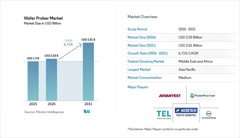
晶圓探針市場預計到 2026 年將價值 20.3 億美元,高於 2025 年的 19 億美元,預計到 2031 年將達到 28.1 億美元。
預計從 2026 年到 2031 年,其複合年成長率將達到 6.71%。
這一強勁成長直接得益於半導體產業產能的擴張以及封裝前對日益小型化、功能更強大的晶片檢驗的需求。先進封裝技術的廣泛應用、人工智慧和5G設備生產的激增以及晶圓尺寸的增大,都在推動對下一代晶圓探針台的需求。供應商正透過將人工智慧整合到故障檢測中、整合預測性維護以及提高探針卡精度,在提高吞吐量的同時降低測試成本,從而滿足這一需求。 2024年,全自動晶圓探針台將佔據市場主導地位,市佔率達64.1%。這得歸功於旨在實現無人值守生產的工廠級自動化項目。接觸式探針台仍主導日常測試領域,市佔率高達87.2%,但非接觸式射頻解決方案正在迅速發展,以支援太赫茲以下裝置。
全球晶圓探針台市場趨勢及洞察
3D積體電路和先進封裝技術快速成長
晶片級架構和異質整合技術的廣泛應用正在重新定義測試需求。多晶片堆疊技術的引入創造了高密度垂直互連,並帶來了傳統晶圓探針台設計無法完全應對的新型可靠性查核點。探針卡供應商目前正在部署高引腳數的MEMS陣列,每次接觸可實現數千個觸點,以覆蓋大面積的中介層表面。 FormFactor公司為先進封裝技術量身訂製的探針卡展示如何透過同時測試多個晶片來縮短測試時間並確保訊號完整性。因此,晶圓探針台市場正朝著高密度、溫度可控且穩定性高達±50 mK的平台方向發展,確保為高功耗AI加速器提供一致的測量結果。
AI/5G設備產量激增。
人工智慧處理器和5G晶片組的爆炸性成長要求晶圓廠在不犧牲利潤率的前提下,大幅提高每小時的裝置測試數量。最新的人工智慧SoC將探針焊盤推至晶片邊緣,並整合了高頻寬記憶體堆疊,這需要50µm的間距均勻性。全自動探針台能夠在每片晶圓上不到兩秒的時間內完成自校準,如今已成為大規模生產線的核心設備。 《半導體工程》指出,以人工智慧為中心的測試需要在探針卡、處理單元和ATE層級進行平行處理,而這種模式會增加功耗和資料登錄的複雜性。供應商正在透過實施基於機器學習的調度和晶圓路由,將測試任務分配到擁塞程度最低的探針台,從而最大限度地提高整體設備效率(OEE)。
高額資本投入和較長的投資回收期
新一代全自動探針台通常每台售價超過300萬美元,對中小晶圓廠的現金流帶來壓力。製程節點的日益複雜要求同時投資探針卡和資料分析平台,從而延長了設備的折舊免稅額週期。根據EPD Tech估計,7奈米及以下製程的製造成本超過10億美元,投資回報期超過24個月。因此,晶圓探針台市場正在轉變,企業傾向於推遲購買,轉而採用租賃模式,按測試的晶圓數量支付費用,從而將資本支出轉化為營運支出。
細分市場分析
預計2025年,全自動晶圓探針台將佔據晶圓探針台市場63.52%的佔有率,複合年成長率(CAGR)為8.91%。供應商正在整合機器人晶圓裝載機、視覺引導對準以及與晶圓廠MES系統無縫整合的SECS/GEM介面。榮獲中國半導體展產品創新獎的SEMISHARE A12工作站,在WAT、CP和RF掃描中均實現了亞微米級的步長精度。韓國和台灣的晶圓廠採用節省人力成本的方案,實現了7x24小時不間斷的設備運行,運轉率超過90%。
半自動設備在中等產量生產線中仍佔有一席之地,因為在這些生產線中,柔軟性至關重要,即使週期時間並非關鍵因素。手動探針雖然出貨量較小,但在大學實驗室和初始裝置表徵中仍然是標準配置,因為在這些應用中,快速接觸焊盤比自動更換晶圓的速度更為重要。
到2025年,接觸式探針將佔銷售額的86.55%,這得益於成熟的探針卡生態系統和可靠的電氣性能。然而,非接觸式方法目前是研發的重點,預計其複合年成長率將達到13.56%。發表在IEEE Transactions上的一項研究介紹了一種介質波導耦合器,該耦合器無需物理引腳即可實現0 Hz至340 GHz的連續覆蓋。無線射頻系統可防止探針標記損壞,並增加重複探測次數,這對於易碎的化合物半導體晶圓而言是一項顯著優勢。
在晶圓探針市場,隨著 6G 原型機的頻率超過 100 GHz,出現了能夠在一次接觸中執行直流參數測量和遠場輻射掃描的試驗單元。
區域分析
亞太地區擁有台灣、韓國和中國當地等密集的晶圓廠叢集,預計2025年將佔據晶圓探針市場47.05%的佔有率。僅台積電一家,其2024年第四季銷售額的74%就來自7奈米及更精細的製程節點,進一步凸顯了該地區向尖端製程節點的轉型。各地政府正推出稅收優惠和電力補貼等政策,鼓勵產能進一步擴張,國內探針卡廠商也努力縮短供貨前置作業時間。
中東和非洲地區以11.24%的複合年成長率呈現最快成長勢頭,沙烏地阿拉伯斥資1000億美元的「Alat」舉措旨在到2030年吸引至少50家設計公司。阿拉伯聯合大公國憑藉其自由區優惠政策吸引企業,有報告稱台積電正在考慮在阿拉伯聯合大公國建立一個類似其亞利桑那州基地的分支機構。當地對人工智慧和國防晶片的需求促使新建實驗室配備中型探針台,這些探針台專為200毫米啟動生產線而最佳化。
北美正受惠於總額達527億美元的《晶片法案》(CHIPS Act),並計畫建立一個專注於300毫米製程的研發中心。亞利桑那州立大學研究園區將設立一個旗艦級的前端製造和先進封裝測試平台。歐洲則透過《歐洲晶片法案》(European Chips Act)尋求自主發展,該法案津貼用於德國、法國和愛爾蘭的探針台現代化改造。這些措施旨在共同減少對亞洲進口的依賴,並使晶圓探針台市場的收入來源多元化。
其他好處:
- Excel格式的市場預測(ME)表
- 3個月的分析師支持
目錄
第1章:引言
- 研究假設和市場定義
- 調查範圍
第2章:調查方法
第3章執行摘要
第4章 市場狀況
- 市場概覽
- 市場促進因素
- 3D積體電路和先進封裝技術的蓬勃發展
- AI/5G設備出貨量增加
- 向 200 毫米和 300 毫米晶圓廠過渡
- SiC/GaN功率元件的大規模生產擴張
- 對各國(美國/歐盟)半導體製造廠的補貼
- 採用MEMS微探針陣列
- 市場限制因素
- 高額資本投入和較長的投資回收期
- 每個高階節點的測試時間增加
- 高精度探針卡供應瓶頸
- 微影術進程內線上測試的替代方案
- 價值鏈分析
- 監理情勢
- 技術展望
- 波特五力分析
- 供應商的議價能力
- 買方的議價能力
- 新進入者的威脅
- 替代品的威脅
- 競爭公司之間的競爭
- 宏觀經濟因素的影響
第5章 市場規模與成長預測
- 依產品類型
- 手動的
- 半自動
- 全自動
- 透過技術
- 聯繫類型
- 非接觸式/無線(無線射頻)
- 透過使用
- 晶圓分選/CP
- 軟體包層級的最終測試
- 研究與開發/故障分析
- 按晶圓尺寸
- 150毫米或更小
- 150~200 mm
- 200~300 mm
- >300 毫米(450 毫米,面板)
- 最終用戶
- 鑄造廠
- IDM
- OSAT
- 研究與學術
- 按地區
- 北美洲
- 美國
- 加拿大
- 墨西哥
- 南美洲
- 巴西
- 阿根廷
- 南美洲其他地區
- 歐洲
- 德國
- 英國
- 法國
- 義大利
- 西班牙
- 俄羅斯
- 其他歐洲地區
- 亞太地區
- 中國
- 日本
- 印度
- 韓國
- 東南亞
- 亞太其他地區
- 中東和非洲
- 中東
- 沙烏地阿拉伯
- 阿拉伯聯合大公國
- 土耳其
- 其他中東國家
- 非洲
- 南非
- 奈及利亞
- 其他非洲地區
- 中東
- 北美洲
第6章 競爭情勢
- 市場集中度
- 策略趨勢
- 市佔率分析
- 公司簡介
- Tokyo Electron Ltd
- Advantest Corp
- FormFactor Inc
- SemiShare Co Ltd
- Micronics Japan Co Ltd
- Accretech(Tokyo Seimitsu)
- MPI Corp
- Wentworth Laboratories Inc
- Technoprobe SpA
- TSE Co Ltd
- Semics Inc
- EverBeing Int'l Corp
- Signatone Corp
- MicroXact Inc
- SEMICAPS Pte Ltd
- Feinmetall GmbH
- INGUN Prufmittelbau GmbH
- SV Probe Pte Ltd
- Chunghwa Precision Test Tech
- Suragus GmbH
- Wuxi Junr Technology Co., Ltd.(JUNR)
- China Micro Semicon Equip(CSEM)
- Signatone Corp
- Tipronics Co Ltd
- STAr Technologies Inc.
- Shibasoku Co Ltd
第7章 市場機會與未來展望
The wafer prober market size in 2026 is estimated at USD 2.03 billion, growing from 2025 value of USD 1.90 billion with 2031 projections showing USD 2.81 billion, growing at 6.71% CAGR over 2026-2031.
This solid growth links directly to the semiconductor sector's rising production capacity and the need to validate ever-smaller, higher-performance chips before packaging. High-volume adoption of advanced packaging, the surge in AI and 5G device output, and the transition to larger wafer formats each reinforce demand for next-generation wafer probers. Vendors are responding by embedding AI in fault detection, integrating predictive maintenance, and improving probe-card precision to keep throughput high and test costs low. The fully automatic segment leads with a 64.1% wafer prober market share in 2024, aided by factory-wide automation programs that target lights-out manufacturing. Contact-based probers still dominate day-to-day test floors, holding 87.2% share, yet non-contact RF solutions are scaling fast to support sub-THz devices.
Global Wafer Prober Market Trends and Insights
3-D IC and Advanced Packaging Boom
Widespread adoption of chiplet architectures and heterogeneous integration is reshaping test requirements. Multidie stacking introduces dense vertical interconnects and new reliability checkpoints that traditional wafer prober designs cannot wholly address. Probe-card suppliers now deploy high-pin-count MEMS arrays that reach thousands of contacts per touchdown to cover large interposer surfaces. FormFactor's custom cards for advanced packages illustrate how simultaneous testing of multiple dies cuts test time while safeguarding signal integrity. The wafer prober market is thus pivoting to high-density, thermally controlled platens capable of +- 50 mK stability, ensuring consistent measurements for power-hungry AI accelerators.
AI / 5G Device Volume Upswing
The explosion of AI processors and 5G chipsets pressures fabs to test far more devices per hour without sacrificing margin. Modern AI SOCs integrate high-bandwidth memory stacks that push probe pads to the edge of the die and demand 50 µm pitch uniformity. Fully automatic probers that self-calibrate alignment in under 2 s per wafer are now central to mass-production lines. Semiconductor Engineering notes that AI-centric testing requires parallelism at the probe card, handler, and ATE levels, a paradigm that raises both current draw and data-logging complexity. Suppliers are adding machine-learning-based scheduling to route wafers to the least congested probers, maximizing overall equipment effectiveness.
High Cap-ex and Long Pay-back
Next-generation fully automatic probers routinely cross USD 3 million per unit, straining cash flow among smaller fabs. Equipment depreciation timelines have stretched as node complexity forces parallel investments in probe cards and data-analytic platforms. EPD Tech calculates that sub-7 nm production costs have topped USD 1 billion, extending ROI horizons beyond 24 months. The wafer prober market thus witnesses deferred purchases or lease models where manufacturers pay by the tested wafer, shifting cap-ex to op-ex.
Other drivers and restraints analyzed in the detailed report include:
- Migration to 200- and 300 mm Fabs
- SiC / GaN Power-Device Ramp-up
- Rising Test-Time per Advanced Node
For complete list of drivers and restraints, kindly check the Table Of Contents.
Segment Analysis
The fully automatic class held a commanding 63.52% wafer prober market share in 2025 and is forecast to post a 8.91% CAGR. Vendors embed robotic wafer loaders, vision-guided alignment, and SECS/GEM interfaces that connect seamlessly with fab MES systems. The SEMISHARE A12 station, recipient of SEMICON China's product innovation award, illustrates step-size accuracy below 1 µm across WAT, CP, and RF sweeps. Labor-light fabs in Korea and Taiwan schedule fleet operation around the clock, lifting utilization rates above 90%.
Semi-automatic units retain a foothold in mid-volume product lines where cycle time is less critical, but flexibility is prized. Manual probes, though small in shipment volume, remain staples in university labs and early device characterization, where quick pad access outweighs automatic wafer exchange speeds.
Contact-based probing still captured 86.55% of 2025 revenue thanks to mature probe-card ecosystems and proven electrical performance. Yet non-contact methods posted a 13.56% CAGR and are now the hottest R&D focus. An IEEE Transactions study described dielectric waveguide couplers that deliver continuous 0 Hz-340 GHz coverage without physical pins. RF-over-air systems avoid probe-mark damage and enable higher reprobing cycles, a major plus for fragile compound-semiconductor wafers.
Probe-card leaders respond with hybrid offerings: vertical MEMS springs for power rails and contactless couplers for millimeter-wave nets on the same card. As 6G prototypes move above 100 GHz, the wafer prober market sees pilot cells that perform DC parametrics and far-field radiation sweeps in a single touchdown.
Wafer Prober Market is Segmented by Product Type (Manual, Semi-Automatic, and Fully Automatic), Technology (Contact, and Non-Contact), Application (Wafer Sort / CP, Package-Level Final Test, and R&D / Failure Analysis), Wafer Size (<=150 Mm, 150-200 Mm, 200-300 Mm, and More), End-User (Foundries, Idms, Osats, and Research and Academia), and Geography (North America, South America, Europe, Asia-Pacific, and Middle East and Africa).
Geography Analysis
Asia-Pacific held 47.05% of the wafer prober market size in 2025, powered by the dense fab clusters of Taiwan, South Korea, and mainland China. TSMC alone reported 74% of Q4 2024 revenue from 7 nm and finer geometries, reinforcing the regional tilt toward cutting-edge nodes. Regional governments offer tax holidays and electricity subsidies that encourage further capacity builds, while domestic probe-card vendors shorten supply lead times.
The Middle East and Africa show the fastest trajectory at an 11.24% CAGR, with Saudi Arabia's USD 100 billion Alat initiative targeting at least 50 design houses by 2030. The UAE courts are founded with free-zone incentives, and reports suggest TSMC is evaluating a UAE site that mirrors its Arizona model. Local demand for AI and defense chips translates into greenfield labs equipped with mid-range probers optimized for 200 mm startup lines.
North America benefits from the USD 52.7 billion CHIPS Act and a pipeline of 300 mm-focused R&D centers. The Arizona State University Research Park will host a flagship testbed for front-end manufacturing and advanced packaging. Europe pursues autonomy via the European Chips Act, allocating grants that modernize probe capacity in Germany, France, and Ireland. Collectively, these initiatives aim to curb reliance on Asian imports and diversify the wafer prober market's revenue base.
- Tokyo Electron Ltd
- Advantest Corp
- FormFactor Inc
- SemiShare Co Ltd
- Micronics Japan Co Ltd
- Accretech (Tokyo Seimitsu)
- MPI Corp
- Wentworth Laboratories Inc
- Technoprobe S.p.A.
- TSE Co Ltd
- Semics Inc
- EverBeing Int'l Corp
- Signatone Corp
- MicroXact Inc
- SEMICAPS Pte Ltd
- Feinmetall GmbH
- INGUN Prufmittelbau GmbH
- SV Probe Pte Ltd
- Chunghwa Precision Test Tech
- Suragus GmbH
- Wuxi Junr Technology Co., Ltd. (JUNR)
- China Micro Semicon Equip (CSEM)
- Signatone Corp
- Tipronics Co Ltd
- STAr Technologies Inc.
- Shibasoku Co Ltd
Additional Benefits:
- The market estimate (ME) sheet in Excel format
- 3 months of analyst support
TABLE OF CONTENTS
1 INTRODUCTION
- 1.1 Study Assumptions and Market Definition
- 1.2 Scope of the Study
2 RESEARCH METHODOLOGY
3 EXECUTIVE SUMMARY
4 MARKET LANDSCAPE
- 4.1 Market Overview
- 4.2 Market Drivers
- 4.2.1 3-D IC and Advanced Packaging Boom
- 4.2.2 AI / 5 G Device Volume Upswing
- 4.2.3 Migration to 200- and 300-mm Fabs
- 4.2.4 SiC / GaN Power-Device Ramp-up
- 4.2.5 National Chip-Fab Subsidies (US/EU)
- 4.2.6 MEMS Micro-probe Array Adoption
- 4.3 Market Restraints
- 4.3.1 High Cap-ex and Long Pay-back
- 4.3.2 Rising Test-time per Advanced Node
- 4.3.3 Precision Probe-Card Supply Bottlenecks
- 4.3.4 In-situ Litho-Stage Test Alternatives
- 4.4 Value Chain Analysis
- 4.5 Regulatory Landscape
- 4.6 Technological Outlook
- 4.7 Porter's Five Forces Analysis
- 4.7.1 Bargaining Power of Suppliers
- 4.7.2 Bargaining Power of Buyers
- 4.7.3 Threat of New Entrants
- 4.7.4 Threat of Substitutes
- 4.7.5 Competitive Rivalry
- 4.8 Impact of Macroeconomic Factors
5 MARKET SIZE AND GROWTH FORECASTS (VALUE)
- 5.1 By Product Type
- 5.1.1 Manual
- 5.1.2 Semi-Automatic
- 5.1.3 Fully Automatic
- 5.2 By Technology
- 5.2.1 Contact
- 5.2.2 Non-contact / RF-over-Air
- 5.3 By Application
- 5.3.1 Wafer Sort / CP
- 5.3.2 Package-Level Final Test
- 5.3.3 R&D / Failure Analysis
- 5.4 By Wafer Size
- 5.4.1 <=150 mm
- 5.4.2 150-200 mm
- 5.4.3 200-300 mm
- 5.4.4 >300 mm (450 mm, Panel)
- 5.5 By End-user
- 5.5.1 Foundries
- 5.5.2 IDMs
- 5.5.3 OSATs
- 5.5.4 Research and Academia
- 5.6 By Geography
- 5.6.1 North America
- 5.6.1.1 United States
- 5.6.1.2 Canada
- 5.6.1.3 Mexico
- 5.6.2 South America
- 5.6.2.1 Brazil
- 5.6.2.2 Argentina
- 5.6.2.3 Rest of South America
- 5.6.3 Europe
- 5.6.3.1 Germany
- 5.6.3.2 United Kingdom
- 5.6.3.3 France
- 5.6.3.4 Italy
- 5.6.3.5 Spain
- 5.6.3.6 Russia
- 5.6.3.7 Rest of Europe
- 5.6.4 Asia-Pacific
- 5.6.4.1 China
- 5.6.4.2 Japan
- 5.6.4.3 India
- 5.6.4.4 South Korea
- 5.6.4.5 South-East Asia
- 5.6.4.6 Rest of Asia-Pacific
- 5.6.5 Middle East and Africa
- 5.6.5.1 Middle East
- 5.6.5.1.1 Saudi Arabia
- 5.6.5.1.2 United Arab Emirates
- 5.6.5.1.3 Turkey
- 5.6.5.1.4 Rest of Middle East
- 5.6.5.2 Africa
- 5.6.5.2.1 South Africa
- 5.6.5.2.2 Nigeria
- 5.6.5.2.3 Rest of Africa
- 5.6.5.1 Middle East
- 5.6.1 North America
6 COMPETITIVE LANDSCAPE
- 6.1 Market Concentration
- 6.2 Strategic Moves
- 6.3 Market Share Analysis
- 6.4 Company Profiles (includes Global-level Overview, Market-level Overview, Core Segments, Financials, Strategic Info, Market Rank/Share, Products and Services, Recent Developments)
- 6.4.1 Tokyo Electron Ltd
- 6.4.2 Advantest Corp
- 6.4.3 FormFactor Inc
- 6.4.4 SemiShare Co Ltd
- 6.4.5 Micronics Japan Co Ltd
- 6.4.6 Accretech (Tokyo Seimitsu)
- 6.4.7 MPI Corp
- 6.4.8 Wentworth Laboratories Inc
- 6.4.9 Technoprobe S.p.A.
- 6.4.10 TSE Co Ltd
- 6.4.11 Semics Inc
- 6.4.12 EverBeing Int'l Corp
- 6.4.13 Signatone Corp
- 6.4.14 MicroXact Inc
- 6.4.15 SEMICAPS Pte Ltd
- 6.4.16 Feinmetall GmbH
- 6.4.17 INGUN Prufmittelbau GmbH
- 6.4.18 SV Probe Pte Ltd
- 6.4.19 Chunghwa Precision Test Tech
- 6.4.20 Suragus GmbH
- 6.4.21 Wuxi Junr Technology Co., Ltd. (JUNR)
- 6.4.22 China Micro Semicon Equip (CSEM)
- 6.4.23 Signatone Corp
- 6.4.24 Tipronics Co Ltd
- 6.4.25 STAr Technologies Inc.
- 6.4.26 Shibasoku Co Ltd
7 MARKET OPPORTUNITIES AND FUTURE OUTLOOK
- 7.1 White-space and Unmet-need Assessment
 電子束晶圓檢測系統市場-2026-2032年全球市場預測
 2026-2030年全球半導體晶圓檢測設備市場
 電子束晶圓檢測系統市場報告:按解析度、應用、最終用途和地區分類(2026-2034 年)
 全球電子束晶圓檢測系統市場規模、佔有率、趨勢和成長分析報告(2026-2034年)
 2026 年至 2035 年電子束晶圓檢測系統市場的機會、成長要素、產業趨勢分析與預測。
 全球晶圓檢測和計量系統市場預測至2034年:按產品類型、技術、晶圓類型、分銷管道、應用、最終用戶和地區分類
 2026年全球半導體晶圓檢測設備市場報告晶圓框架市場:依產品類型、晶圓尺寸、材料、生產技術、應用和最終用戶分類,全球預測,2026-2032年
 晶圓級測試和老化(WLTBI)市場:按測試類型、技術、最終用戶行業、國家和地區分類 - 全球行業分析、市場規模、市場佔有率及2025-2032年預測2032年半導體晶圓檢測設備市場預測:按設備類型、晶圓材料、技術、應用、最終用戶和地區進行的全球分析