

 |
市場調查報告書
商品編碼
1959568
2026 年至 2035 年電子束晶圓檢測系統市場的機會、成長要素、產業趨勢分析與預測。E-Beam Wafer Inspection System Market Opportunity, Growth Drivers, Industry Trend Analysis, and Forecast 2026 - 2035 |
||||||
2025 年全球電子束晶圓檢測系統市值為 14 億美元,預計到 2035 年將達到 69 億美元,複合年成長率為 18.3%。
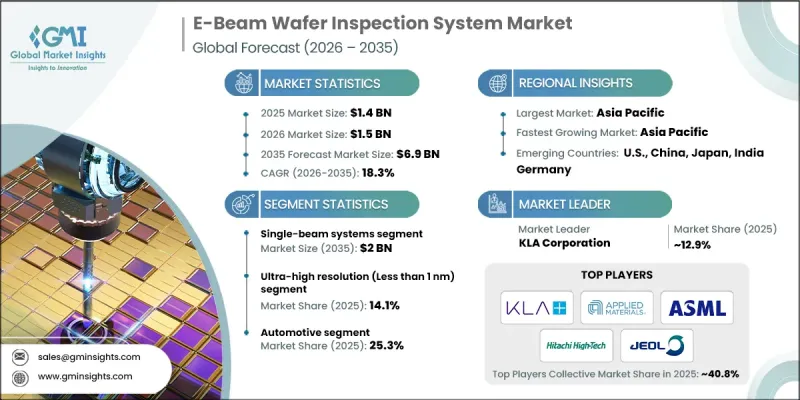
半導體製造產能投資的增加以及先進元件日益複雜化是推動市場成長的主要因素。製造商正在將人工智慧 (AI) 和機器學習 (ML) 演算法整合到其檢測系統中,以提高缺陷檢測率和產量比率。新興技術的蓬勃發展,例如 5G、人工智慧、物聯網 (IoT) 和汽車電子等,對高品質晶圓的需求日益成長,也推動了市場需求。隨著晶圓結構變得越來越複雜,對精密檢測工具的需求也不斷增加,尤其是在家用電子電器、通訊和記憶體製造業。
| 市場範圍 | |
|---|---|
| 開始年份 | 2025 |
| 預測年份 | 2026-2035 |
| 起始值 | 14億美元 |
| 預測金額 | 69億美元 |
| 複合年成長率 | 18.3% |
採用諸如環柵電晶體 (GAA) 和 3D NAND 等先進的 3D 裝置結構,為缺陷表徵帶來了巨大挑戰。複雜的垂直結構和多層堆疊結構超出了光學檢測系統的能力範圍,因此製造商在邏輯和記憶體製造中越來越依賴電子束檢測系統。電子束檢測系統能夠提供高解析度成像並精確識別結構缺陷,從而確保先進半導體製造的品質和可靠性。
預計到2035年,單光束系統市場規模將成長至20億美元,主要得益於其經濟實惠的價格以及對研發和中小規模生產的適應性。這些系統易於部署,同時也能提供高解析度成像,因此是中小型晶圓廠和學術研究機構的理想選擇。在10奈米以下節點實現的缺陷檢測能力有助於提高產量比率和最佳化工藝,從而減少廢棄物並提升整體效率。
解析度低於1奈米的超高解析度成像技術預計到2025年將佔據14.1%的市場。亞奈米成像對於識別低解析度系統無法檢測到的圖形化缺陷、隨機缺陷和材料缺陷至關重要。這項技術在下一代邏輯和儲存裝置以及極微影術程中至關重要,因為即使是原子級的微小缺陷也會對產量比率和裝置性能產生顯著影響。
預計2025年,北美電子束晶圓檢測系統市佔率將達到33.2%。這一成長主要得益於主要半導體製造商、先進製程節點晶圓廠以及EUV微影術的早期應用。加之7奈米以下製程技術的快速普及以及對研發和先進製程控制的大力投入,電子束檢測在缺陷檢測和產量比率管理方面正變得至關重要。供應商與晶圓廠之間的合作正在推動人工智慧驅動的缺陷分析和多束技術的發展,進一步鞏固了北美市場的領先地位。
目錄
第1章:調查方法和範圍
第2章執行摘要
第3章業界考察
- 生態系分析
- 供應商情況
- 利潤率分析
- 成本結構
- 每個階段增加的價值
- 影響價值鏈的因素
- 中斷
- 影響產業的因素
- 促進因素
- 先進節點對缺陷敏感度的要求日益提高
- 擴大半導體代工廠產能
- 3D裝置結構的日益複雜
- EUV微影術的快速普及
- 多束電子束系統的技術進步
- 產業潛在風險與挑戰
- 與光學裝置相比,吞吐量相對較低。
- 將系統整合到晶圓廠工作流程中的複雜性
- 市場機遇
- 訂閱模式和地圖即服務模式的成長
- 在未開發的市場中尋求擴張機會
- 促進因素
- 監理情勢
- 波特五力分析
- PESTEL 分析
- 科技與創新趨勢
- 當前技術趨勢
- 新興技術
- 新興經營模式
- 合規要求
- 專利和智慧財產權分析
- 地緣政治和貿易趨勢
第4章 競爭情勢
- 介紹
- 企業市佔率分析
- 按地區
- 主要企業的競爭標竿分析
- 財務績效比較
- 收入
- 利潤率
- 研究與開發
- 產品系列比較
- 產品線的廣度
- 科技
- 創新
- 地理位置比較
- 全球擴張分析
- 服務網路覆蓋
- 按地區分類的市場滲透率
- 競爭定位矩陣
- 領導企業
- 受讓人
- 追蹤者
- 小眾玩家
- 戰略展望矩陣
- 財務績效比較
- 2022-2025 年重大發展
- 併購
- 合作夥伴關係和合資企業
- 技術進步
- 擴張和投資策略
- 數位轉型計劃
- 新興/Start-Ups競爭對手的發展趨勢
第5章 市場估算與預測:依系統結構,2022-2035年
- 單光束系統
- 多波束系統
第6章 市場估計與預測:依解析度能力分類,2022-2035年
- 超高解析度(小於1奈米)
- 高解析度(1nm-10nm)
- 標準解析度(>10nm)
第7章 市場估價與預測:依製造流程分類,2022-2035年
- 前端晶圓檢測
- 後端晶圓檢測
第8章 市場估算與預測:依最終用戶產業分類,2022-2035年
- 車
- 家用電子電器
- 電訊
- 工業和企業電子設備
- 其他
- 醫療/醫療設備
- 國防/航太電子
第9章 市場估計與預測:依地區分類,2022-2035年
- 北美洲
- 美國
- 加拿大
- 歐洲
- 德國
- 英國
- 法國
- 西班牙
- 義大利
- 荷蘭
- 亞太地區
- 中國
- 印度
- 日本
- 澳洲
- 韓國
- 拉丁美洲
- 巴西
- 墨西哥
- 阿根廷
- 中東和非洲
- 南非
- 沙烏地阿拉伯
- 阿拉伯聯合大公國
第10章:公司簡介
- KLA Corporation
- Applied Materials, Inc.
- ASML Holding NV
- Hitachi High Technologies Corp.
- JEOL Ltd.
- Onto Innovation.
- Carl Zeiss SMT
- Aerotech, Inc.
- MKS Inc.
- PDF Solutions
- Wuhan Jingce Electronic Group
- Thermo Fisher Scientific Inc.
- Camtek
- Advantest Corporation
- SCREEN SPE Tech Co., Ltd.
The Global E-Beam Wafer Inspection System Market was valued at USD 1.4 billion in 2025 and is estimated to grow at a CAGR of 18.3% to reach USD 6.9 billion by 2035.
The market's growth is fueled by rising investments in semiconductor manufacturing capacity and the increasing complexity of advanced devices. Manufacturers are integrating artificial intelligence (AI) and machine learning (ML) algorithms into inspection systems to improve defect detection and yield optimization. Demand is also driven by the proliferation of emerging technologies, including 5G, artificial intelligence, the Internet of Things (IoT), and automotive electronics, all of which require high-quality wafers. As wafer architectures become more intricate, the need for precise inspection tools has grown, particularly in consumer electronics, telecommunications, and memory fabrication industries.
| Market Scope | |
|---|---|
| Start Year | 2025 |
| Forecast Year | 2026-2035 |
| Start Value | $1.4 Billion |
| Forecast Value | $6.9 Billion |
| CAGR | 18.3% |
The adoption of advanced 3D device architectures, such as gate-all-around (GAA) transistors and 3D NAND, is creating significant challenges for defect characterization. Complex vertical structures and multilayer stacking exceed the capabilities of optical inspection systems, prompting manufacturers to rely increasingly on e-beam systems for logic and memory fabrication. E-beam inspection systems offer high-resolution imaging and accurate identification of structural defects, ensuring quality and reliability in advanced semiconductor manufacturing.
The single-beam systems segment is expected to reach USD 2 billion by 2035, driven by their affordability and suitability for research, development, and low- to mid-volume production. These systems provide high-resolution imaging with simpler deployment, making them ideal for small- to medium-scale fabs and academic research centers. Their ability to detect defects in sub-10 nm nodes supports yield learning and process optimization, reducing scrap and improving overall efficiency.
The ultra-high-resolution segment, defined by resolutions below 1 nm, held 14.1% share in 2025. Sub-nanometer imaging is critical for identifying patterning, stochastic, and material defects that lower-resolution systems cannot detect. This capability is essential for next-generation logic and memory devices, as well as EUV lithography processes, where even atomic-scale imperfections can significantly impact yield and device performance.
North America E-Beam Wafer Inspection System Market held a 33.2% share in 2025. The region's growth is supported by the presence of leading semiconductor manufacturers, advanced-node fabs, and early adoption of EUV lithography. High adoption of sub-7 nm processes, coupled with strong investments in R&D and advanced process control, makes e-beam inspection critical for defect detection and yield management. Collaborations between equipment vendors and fabs facilitate AI-driven defect analytics and multi-beam technologies, further reinforcing North America's market leadership.
Prominent players in the Global E-Beam Wafer Inspection System Market include Applied Materials, Inc., KLA Corporation, ASML Holding N.V., Hitachi High Technologies Corp., JEOL Ltd., Onto Innovation, Carl Zeiss SMT, Aerotech, Inc., MKS Inc., PDF Solutions, Thermo Fisher Scientific Inc., Camtek, Advantest Corporation, SCREEN SPE Tech Co., Ltd., and Wuhan Jingce Electronic Group. Companies in the Global E-Beam Wafer Inspection System Market are strengthening their foothold through strategic initiatives such as investing in AI and ML integration to enhance defect detection capabilities, expanding multi-beam system development for higher throughput, and forming partnerships with semiconductor fabs to customize solutions for advanced nodes. They are also focusing on global expansion to tap into emerging markets, enhancing service networks for predictive maintenance, and offering modular, scalable solutions for both high-volume manufacturing and R&D applications. Continuous innovation in sub-nanometer resolution, combined with software-driven process optimization, allows these companies to maintain competitiveness and reinforce long-term market leadership.
Table of Contents
Chapter 1 Methodology and Scope
- 1.1 Market scope and definition
- 1.2 Research design
- 1.2.1 Research approach
- 1.2.2 Data collection methods
- 1.3 Data mining sources
- 1.3.1 Global
- 1.3.2 Regional/Country
- 1.4 Base estimates and calculations
- 1.4.1 Base year calculation
- 1.4.2 Key trends for market estimation
- 1.5 Primary research and validation
- 1.5.1 Primary sources
- 1.6 Forecast model
- 1.7 Research assumptions and limitations
Chapter 2 Executive Summary
- 2.1 Industry 360° synopsis, 2022 - 2035
- 2.2 Key market trends
- 2.2.1 System type trends
- 2.2.2 Deployment model trends
- 2.2.3 End-user industry trends
- 2.2.4 Regional trends
- 2.3 TAM analysis, 2025-2035
- 2.4 CXO perspectives: Strategic imperatives
- 2.4.1 Executive decision points
- 2.4.2 Critical success factors
- 2.5 Future outlook and strategic recommendations
Chapter 3 Industry Insights
- 3.1 Industry ecosystem analysis
- 3.1.1 Supplier landscape
- 3.1.2 Profit margin analysis
- 3.1.3 Cost structure
- 3.1.4 Value addition at each stage
- 3.1.5 Factor affecting the value chain
- 3.1.6 Disruptions
- 3.2 Industry impact forces
- 3.2.1 Growth drivers
- 3.2.1.1 Escalating defect sensitivity requirements in advanced nodes
- 3.2.1.2 Expansion of semiconductor foundry capacity
- 3.2.1.3 Growing complexity of 3d device architectures
- 3.2.1.4 Rapid adoption of EUV lithography
- 3.2.1.5 Technological advancements in multi-beam e-beam systems
- 3.2.2 Industry pitfalls and challenges
- 3.2.2.1 Relatively low throughput compared to optical tools
- 3.2.2.2 Complexity of system integration into fab workflows
- 3.2.3 Market opportunities
- 3.2.3.1 Growth of subscription-based & mapping-as-a-service models
- 3.2.3.2 Expansion opportunities in underpenetrated markets
- 3.2.1 Growth drivers
- 3.3 Regulatory landscape
- 3.3.1 North America
- 3.3.2 Europe
- 3.3.3 Asia Pacific
- 3.3.4 Latin America
- 3.3.5 Middle East & Africa
- 3.4 Porter's analysis
- 3.5 PESTEL analysis
- 3.6 Technology and innovation landscape
- 3.6.1 Current technological trends
- 3.6.2 Emerging technologies
- 3.7 Emerging business models
- 3.8 Compliance requirements
- 3.9 Patent and IP analysis
- 3.10 Geopolitical and trade dynamics
Chapter 4 Competitive Landscape, 2025
- 4.1 Introduction
- 4.2 Company market share analysis
- 4.2.1 By region
- 4.2.1.1 North America
- 4.2.1.2 Europe
- 4.2.1.3 Asia Pacific
- 4.2.1.4 Latin America
- 4.2.1.5 Middle East & Africa
- 4.2.1 By region
- 4.3 Competitive benchmarking of key players
- 4.3.1 Financial performance comparison
- 4.3.1.1 Revenue
- 4.3.1.2 Profit margin
- 4.3.1.3 R&D
- 4.3.2 Product portfolio comparison
- 4.3.2.1 Product range breadth
- 4.3.2.2 Technology
- 4.3.2.3 Innovation
- 4.3.3 Geographic presence comparison
- 4.3.3.1 Global footprint analysis
- 4.3.3.2 Service network coverage
- 4.3.3.3 Market penetration by region
- 4.3.4 Competitive positioning matrix
- 4.3.4.1 Leaders
- 4.3.4.2 Challengers
- 4.3.4.3 Followers
- 4.3.4.4 Niche players
- 4.3.5 Strategic outlook matrix
- 4.3.1 Financial performance comparison
- 4.4 Key developments, 2022-2025
- 4.4.1 Mergers and acquisitions
- 4.4.2 Partnerships and collaborations
- 4.4.3 Technological advancements
- 4.4.4 Expansion and investment strategies
- 4.4.5 Digital transformation initiatives
- 4.5 Emerging/ startup competitors' landscape
Chapter 5 Market Estimates and Forecast, By System Architecture, 2022 - 2035 (USD Million, Units)
- 5.1 Key trends
- 5.2 Single-Beam Systems
- 5.3 Multi-Beam Systems
Chapter 6 Market Estimates and Forecast, By Resolution Capability, 2022 - 2035 (USD Million, Units)
- 6.1 Key trends
- 6.2 Ultra-High Resolution (Less than 1 nm)
- 6.3 High Resolution (1 nm to 10 nm)
- 6.4 Standard Resolution (More than 10 nm)
Chapter 7 Market Estimates and Forecast, By Process Stage, 2022 - 2035 (USD Million, Units)
- 7.1 Key trends
- 7.2 Front-End Wafer Inspection
- 7.3 Back-End Wafer Inspection
Chapter 8 Market Estimates and Forecast, By End-User Industry, 2022 - 2035 (USD Million, Units)
- 8.1 Key trends
- 8.2 Automotive
- 8.3 Consumer Electronics
- 8.4 Telecommunications
- 8.5 Industrial & Enterprise Electronics
- 8.6 Others
- 8.6.1 Healthcare / Medical Electronics
- 8.6.2 Defense / Aerospace Electronics
Chapter 9 Market Estimates and Forecast, By Region, 2022 - 2035 (USD Mn)
- 9.1 Key trends
- 9.2 North America
- 9.2.1 U.S.
- 9.2.2 Canada
- 9.3 Europe
- 9.3.1 Germany
- 9.3.2 UK
- 9.3.3 France
- 9.3.4 Spain
- 9.3.5 Italy
- 9.3.6 Netherlands
- 9.4 Asia Pacific
- 9.4.1 China
- 9.4.2 India
- 9.4.3 Japan
- 9.4.4 Australia
- 9.4.5 South Korea
- 9.5 Latin America
- 9.5.1 Brazil
- 9.5.2 Mexico
- 9.5.3 Argentina
- 9.6 Middle East and Africa
- 9.6.1 South Africa
- 9.6.2 Saudi Arabia
- 9.6.3 UAE
Chapter 10 Company Profiles
- 10.1 KLA Corporation
- 10.2 Applied Materials, Inc.
- 10.3 ASML Holding N.V.
- 10.4 Hitachi High Technologies Corp.
- 10.5 JEOL Ltd.
- 10.6 Onto Innovation.
- 10.7 Carl Zeiss SMT
- 10.8 Aerotech, Inc.
- 10.9 MKS Inc.
- 10.10 PDF Solutions
- 10.11 Wuhan Jingce Electronic Group
- 10.12 Thermo Fisher Scientific Inc.
- 10.13 Camtek
- 10.14 Advantest Corporation
- 10.15 SCREEN SPE Tech Co., Ltd.
 2026-2030年全球半導體晶圓檢測設備市場
 電子束晶圓檢測系統市場報告:按解析度、應用、最終用途和地區分類(2026-2034 年)
 電子束晶圓檢測系統市場:2026-2032年全球市場預測(依積體電路、光電、檢測技術、晶圓尺寸、應用和最終用戶產業分類)
 全球電子束晶圓檢測系統市場規模、佔有率、趨勢和成長分析報告(2026-2034年)
 全球晶圓檢測和計量系統市場預測至2034年:按產品類型、技術、晶圓類型、分銷管道、應用、最終用戶和地區分類
 晶圓驗證儀:市場佔有率分析、行業趨勢和統計數據、成長預測(2026-2031 年)
 2026年全球半導體晶圓檢測設備市場報告晶圓框架市場:依產品類型、晶圓尺寸、材料、生產技術、應用和最終用戶分類,全球預測,2026-2032年
 晶圓級測試和老化(WLTBI)市場:按測試類型、技術、最終用戶行業、國家和地區分類 - 全球行業分析、市場規模、市場佔有率及2025-2032年預測2032年半導體晶圓檢測設備市場預測:按設備類型、晶圓材料、技術、應用、最終用戶和地區進行的全球分析