


 |
市場調查報告書
商品編碼
1940697
半導體微影術設備:市場佔有率分析、產業趨勢與統計、成長預測(2026-2031)Semiconductor Lithography Equipment - Market Share Analysis, Industry Trends & Statistics, Growth Forecasts (2026 - 2031) |
||||||
※ 本網頁內容可能與最新版本有所差異。詳細情況請與我們聯繫。
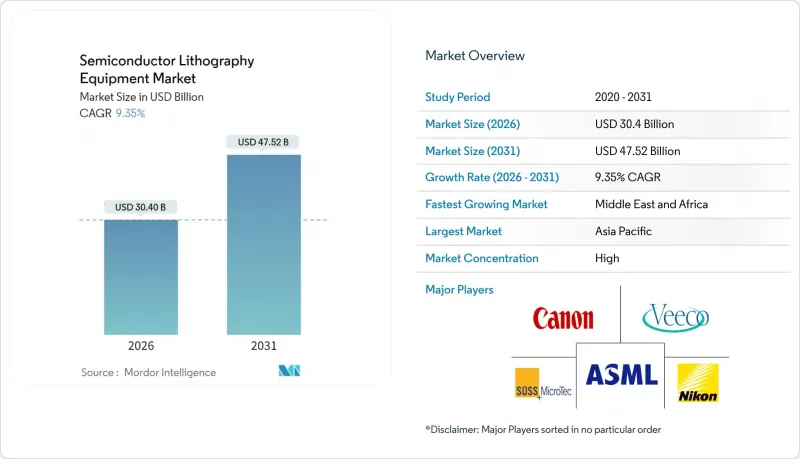
預計半導體微影術設備市場將從 2025 年的 278 億美元成長到 2026 年的 304 億美元,到 2031 年達到 475.2 億美元,2026 年至 2031 年的複合年成長率為 9.35%。
這一成長勢頭主要得益於向極紫外線 (EUV) 光刻技術的轉型以及即將推出的高數值孔徑 (高NA) EUV 平台、人工智慧伺服器的普及以及需要更高密度圖形化精度的兆電晶體圖形加速器的出現。亞太地區仍是製造業產能擴張的關鍵驅動力,這主要得益於台灣晶圓代工的優勢以及韓國高達 4,710 億美元的超級產業叢集計畫。雖然深紫外線 (DUV) 設備作為成熟製程節點的基礎仍然至關重要,但高數值孔徑 EUV 設備的訂單量表明,整個生態系統正在迅速轉型為 1 奈米以下製程。儘管資本投資強度和出口限制仍然是推廣應用的主要障礙,但政府補貼、封裝創新和節能設備設計正在共同推動先進曝光系統的應用範圍不斷擴大。
全球半導體微影術設備市場趨勢與洞察
小型化製程推動了EUV技術的應用
電晶體密度的不斷提高推動了對7奈米以下微縮製程的需求,而這只有極紫外光刻(EUV)才能實現。台積電在其新竹工廠成功實現了高數值孔徑(NA)光刻機的首次光刻,為2030年實現1奈米製程的量產做準備。 ASML的EXE平台採用變形光學元件實現了8奈米解析度,與先前的NXE型號相比,影像對比度提高了40%。調查團隊已實現了5奈米線間距的干涉曝光,證實了其性能遠低於藍圖。預計伺服器級處理器的電晶體數量將加倍,達到2000億個,這將進一步推高光刻產能的需求。這些里程碑事件凸顯了埃級微縮製程的快速發展,並將高數值孔徑光刻機確立為最重要的資本投資項目。
人工智慧和資料中心對尖端晶片的需求
人工智慧伺服器需要擁有超過2兆個電晶體的多晶片GPU。預計到2030年,半導體銷售額將超過1兆美元,其中人工智慧加速器和高頻寬記憶體將成為關鍵的成長引擎。諸如CoWoS等先進封裝技術對線路重布的微影術套刻精度提出了更高的要求。三星的異質整合藍圖和台積電的CoWoS產能擴張正在推動大尺寸曝光設備的緊急徵兆。阿布達比擁有1-5GW人工智慧運算叢集,配備數十萬個GPU,標誌著一個新地區進入了資本支出週期。
EUV曝光設備需要極高的資本投入
ASML的高數值孔徑(高NA)光刻機每台造價高達3.8億美元,是早期EUV平台價格的兩倍。潔淨室改造、隔振以及兆瓦級的電力和冷卻設備進一步增加了總擁有成本。預計到2025年底,全球將安裝不到20台高NA光刻機,中型晶圓廠將無緣參與這場埃級光刻競賽。沖繩科學技術大學院大學(OIST)的一項研究提案了雙鏡投影機和20瓦光源的方案,該方案有望將電力消耗降低90%,從而可能減輕未來的資本支出。
細分市場分析
到2025年,DUV平台將維持56.10%的半導體微影術設備市場佔有率,凸顯了其在成熟節點和成本敏感型生產線上的重要性。高數值孔徑EUV目前在半導體微影術設備市場中所佔佔有率較小,但預計到2031年將以10.54%的複合年成長率成長,屆時單次曝光1nm成像將成為量產現實。 ASML EXE系列中的0.55 NA變形投影技術提高了景深,實現了以往無需四重圖形化即可達到的缺陷密度目標。 Imec在20nm間距金屬線上實現了90%的電氣產量比率,證實了其已做好量產準備。
傳統極紫外光刻技術對於5nm邏輯晶片、 NAND快閃記憶體和DRAM更新仍然至關重要,0.33數值孔徑(NA)可提供可接受的套刻精度,並支援多重圖形化。深紫外線浸沒式微影技術已在許多晶圓廠實現成本攤銷,在類比、射頻和MEMS製程中仍保持著晶粒優勢。Canon的奈米壓印試驗線和尼康的浸沒式光刻技術改進表明,在細分市場存在競爭,但ASML對以光罩格式為中心的生態系統的依賴,鞏固了其平台優勢。
區域分析
亞太地區預計到2025年將佔67.60%的市場佔有率,這反映了邏輯和記憶體超大型晶圓廠集中在台灣、韓國、日本和中國當地。韓國價值4,710億美元的叢集正在增加多台極紫外光刻機,而日本政府的支持也促使台積電在熊本建設第二座晶圓廠。儘管受到出口限制,但隨著國內光刻計劃的擴張,中國在2024年仍將在晶圓廠設備方面投入490億美元。
北美位居第二,在《晶片技術創新法案》(CHIPS Act)的聯合資助下,英特爾、台積電和三星在美國的計劃投資額超過2,000億美元。光是亞利桑那州的雙晶圓廠園區在預測期內就將安裝超過25台極紫外光刻設備。奧勒岡、俄亥俄州和德克薩斯的晶圓廠叢集將擴大地理冗餘度,從而增強該地區對設備服務的需求。
中東和非洲地區雖然目前規模較小,但年複合成長率高達12.48%。沙烏地阿拉伯10億沙烏地里亞爾的創投基金正在支持建造國家半導體中心,而阿拉伯聯合大公國的資料中心計劃也需要在地化的先進封裝技術。政府間的技術轉移協議有助於加快專案進度,但勞動力和供應鏈深度仍是發展的瓶頸。
其他福利:
- Excel格式的市場預測(ME)表
- 3個月的分析師支持
目錄
第1章 引言
- 研究假設和市場定義
- 調查範圍
第2章調查方法
第3章執行摘要
第4章 市場情勢
- 市場概覽
- 市場促進因素
- 製程節點尺寸縮小推動了EUV技術的應用
- 人工智慧和資料中心對尖端晶片的需求
- 政府晶圓廠補貼(例如,晶片法案)
- 先進封裝(2.5D/3D IC)的快速成長
- 高數值孔徑 EUV 光刻更新率加快設備週期
- 化合物半導體光刻需求
- 市場限制
- EUV掃描器的資本投資極為昂貴
- 子系統供應鏈瓶頸
- 永續性和能源利用面臨的壓力
- 對華出口管制條例
- 價值鏈分析
- 監管環境
- 技術展望
- 波特五力分析
- 新進入者的威脅
- 供應商的議價能力
- 買方的議價能力
- 替代品的威脅
- 競爭對手之間的競爭
- 定價分析
- 宏觀經濟因素的影響
第5章 市場規模與成長預測
- 透過印刷方法
- 深紫外線(DUV)
- 極紫外線(EUV)
- 高數值孔徑極紫外光刻
- 透過使用
- 先進包裝
- MEMS元件
- LED元件
- 功率半導體和化合物半導體
- 最終用戶
- 專業鑄造廠
- 整合裝置製造商(IDM)
- 半導體外包組裝和測試服務 (OSAT)
- 按地區
- 北美洲
- 美國
- 加拿大
- 墨西哥
- 南美洲
- 巴西
- 阿根廷
- 南美洲其他地區
- 歐洲
- 德國
- 英國
- 法國
- 義大利
- 西班牙
- 俄羅斯
- 其他歐洲地區
- 亞太地區
- 中國
- 日本
- 印度
- 韓國
- 東南亞
- 亞太其他地區
- 中東和非洲
- 中東
- 沙烏地阿拉伯
- 阿拉伯聯合大公國
- 土耳其
- 其他中東地區
- 非洲
- 南非
- 奈及利亞
- 其他非洲地區
- 中東
- 北美洲
第6章 競爭情勢
- 市場集中度
- 策略趨勢
- 市佔率分析
- 公司簡介
- ASML Holding NV
- Nikon Corporation
- Canon Inc.
- Shanghai Micro Electronics Equipment(Group)Co., Ltd.
- SUSS MicroTec SE
- EV Group
- Veeco Instruments Inc.
- Onto Innovation Inc.
- JEOL Ltd.
- Neutronix Quintel Inc.
- Mycronic AB
- NuFlare Technology Inc.
- Ushio Inc.
- Ultratech(Veeco)
- Mapper Lithography BV
- Visitech AS
- KLA Corporation
- MKS Instruments(Newport)
- Inpria Corp.
- Tamarack Scientific Co.
第7章 市場機會與未來展望
The semiconductor lithography equipment market is expected to grow from USD 27.8 billion in 2025 to USD 30.4 billion in 2026 and is forecast to reach USD 47.52 billion by 2031 at 9.35% CAGR over 2026-2031.
Momentum stems from the shift toward extreme ultraviolet (EUV) and forthcoming High-NA EUV platforms, the surge in artificial-intelligence servers, and multi-trillion-transistor graphics accelerators that demand denser patterning precision. Asia-Pacific remains the fulcrum of manufacturing capacity expansions, led by Taiwan's foundry dominance and South Korea's USD 471 billion mega-cluster program. Deep-ultraviolet (DUV) tools still anchor mature nodes, but the pipeline of High-NA EUV orders shows how quickly the ecosystem is pivoting toward sub-1 nm production. Capital-expenditure intensity and export-control compliance are the main brakes on diffusion, yet government subsidies, packaging innovations, and energy-efficient tool designs together widen the addressable base for advanced exposure systems.
Global Semiconductor Lithography Equipment Market Trends and Insights
Shrinking Process Nodes Drive EUV Adoption
Growing transistor density forces sub-7 nm geometries that only EUV can achieve. TSMC recorded first light on a High-NA tool in Hsinchu as it prepares 1 nm mass output by 2030. ASML's EXE platform reaches 8 nm resolution with anamorphic optics, a 40% imaging-contrast jump over prior NXE models. Research teams demonstrated 5 nm line-space interference printing, confirming far-below-roadmap capability. Server-class processors are projected to double to 200 billion transistors, magnifying lithography throughput needs. These milestones underline a rapid cadence toward angstrom dimensions that places High-NA tools at the center of capex priorities.
AI and Data-Center Demand for Leading-Edge Chips
Artificial-intelligence servers require multi-chiplet GPUs pushing past 2 trillion transistors. Semiconductor revenue is modeled to top USD 1 trillion by 2030, with AI accelerators and high-bandwidth memory as primary growth engines. Advanced packaging formats such as CoWoS intensify lithography overlay accuracy for redistribution layers. Samsung's heterogeneous-integration roadmap and TSMC's CoWoS capacity ramp have driven rush orders for large-panel exposure tools. Abu Dhabi's 1-5 GW AI compute cluster, featuring hundreds of thousands of GPUs, signals new geographies entering the capex cycle.
Ultra-High Capex of EUV Scanners
ASML's High-NA units list at USD 380 million each, double the cost of early EUV platforms. Total cost of ownership multiplies after clean-room reconfiguration, vibration isolation, and megawatt-class power-and-cooling utilities. Fewer than 20 High-NA machines are likely installed worldwide by end-2025, leaving mid-tier fabs locked out of the angstrom race. Research at the Okinawa Institute proposes a two-mirror projector and a 20-W source that could shrink power draw by 90%, hinting at future capex relief.
Other drivers and restraints analyzed in the detailed report include:
- Government Fab Subsidies Drive Equipment Investment
- Advanced-Packaging Boom Accelerates Equipment Demand
- Export-Control Restrictions to China
For complete list of drivers and restraints, kindly check the Table Of Contents.
Segment Analysis
In 2025, DUV platforms maintained 56.10% semiconductor lithography equipment market share, underlining their role in mature-node and cost-sensitive lines. High-NA EUV, although a smaller slice of the semiconductor lithography equipment market size today, is forecast to grow 10.54% CAGR through 2031 as single-exposure 1 nm imaging becomes a production reality. The 0.55 NA anamorphic projection inside ASML's EXE series improves depth-of-focus, enabling defect-density targets previously unattainable without quadruple patterning. Imec's 90% electrical yield on 20 nm pitch metal lines corroborates readiness for volume runs.
Conventional EUV remains indispensable for 5 nm logic, NAND flash, and DRAM refreshes, where 0.33 NA offers acceptable overlay with multi-patterning. Deep-UV immersion, already fully depreciated at many fabs, keeps the cost-per-die edge for analog, RF, and MEMS flows. Canon's nano-imprint pilot lines and Nikon's immersion enhancements signal niche competitive threats, yet ecosystem lock-in around ASML reticle formats sustains its platform moat.
The Semiconductor Lithography Machine Manufacturers Market is Segmented by Type (Deep Ultraviolet Lithography and Extreme Ultraviolet Lithography), Application (Advanced Packaging, MEMS Devices, and LED Devices), and Geography (North America, Europe, and More). The Market Forecasts are Provided in Terms of Value (USD).
Geography Analysis
Asia-Pacific's 67.60% share in 2025 reflects the agglomeration of logic and memory megafabs across Taiwan, South Korea, Japan, and mainland China. South Korea's USD 471 billion cluster will add multiple EUV suites, while Japan's government incentives lure TSMC into second-phase Kumamoto construction. China, despite export curbs, still spent USD 49 billion on overall fab tools in 2024 as domestic lithography projects scale.
North America ranks second, fueled by CHIPS Act co-funding that pushes combined Intel, TSMC, and Samsung U.S. projects past USD 200 billion. Arizona's twin-fab campus alone will deploy more than 25 EUV scanners over the forecast horizon. Fab clusters in Oregon, Ohio, and Texas broaden geographic redundancy and strengthen regional tool-service demand.
The Middle East and Africa, though small today, show a 12.48% CAGR. Saudi Arabia's SAR 1 billion venture fund underpins the National Semiconductor Hub, while UAE data-center projects necessitate local advanced-packaging capacity. Government-to-government technology-transfer accords expedite timeline compression, but workforce and supply-chain depth remain developmental bottlenecks.
- ASML Holding N.V.
- Nikon Corporation
- Canon Inc.
- Shanghai Micro Electronics Equipment (Group) Co., Ltd.
- SUSS MicroTec SE
- EV Group
- Veeco Instruments Inc.
- Onto Innovation Inc.
- JEOL Ltd.
- Neutronix Quintel Inc.
- Mycronic AB
- NuFlare Technology Inc.
- Ushio Inc.
- Ultratech (Veeco)
- Mapper Lithography B.V.
- Visitech AS
- KLA Corporation
- MKS Instruments (Newport)
- Inpria Corp.
- Tamarack Scientific Co.
Additional Benefits:
- The market estimate (ME) sheet in Excel format
- 3 months of analyst support
TABLE OF CONTENTS
1 INTRODUCTION
- 1.1 Study Assumptions and Market Definition
- 1.2 Scope of the Study
2 RESEARCH METHODOLOGY
3 EXECUTIVE SUMMARY
4 MARKET LANDSCAPE
- 4.1 Market Overview
- 4.2 Market Drivers
- 4.2.1 Shrinking process nodes drive EUV adoption
- 4.2.2 AI and data-center demand for leading-edge chips
- 4.2.3 Government fab subsidies (e.g., CHIPS Act)
- 4.2.4 Advanced-packaging boom (2.5D/3D IC)
- 4.2.5 High-NA EUV refresh accelerates tool cycles
- 4.2.6 Compound-semiconductor lithography demand
- 4.3 Market Restraints
- 4.3.1 Ultra-high capex of EUV scanners
- 4.3.2 Sub-system supply-chain bottlenecks
- 4.3.3 Sustainability and energy-use pressures
- 4.3.4 Export-control restrictions to China
- 4.4 Value Chain Analysis
- 4.5 Regulatory Landscape
- 4.6 Technological Outlook
- 4.7 Porter's Five Forces Analysis
- 4.7.1 Threat of New Entrants
- 4.7.2 Bargaining Power of Suppliers
- 4.7.3 Bargaining Power of Buyers
- 4.7.4 Threat of Substitutes
- 4.7.5 Competitive Rivalry
- 4.8 Pricing Analysis
- 4.9 Impact of Macroeconomic Factors
5 MARKET SIZE AND GROWTH FORECASTS (VALUE)
- 5.1 By Lithography Type
- 5.1.1 Deep Ultraviolet (DUV)
- 5.1.2 Extreme Ultraviolet (EUV)
- 5.1.3 High-NA EUV
- 5.2 By Application
- 5.2.1 Advanced Packaging
- 5.2.2 MEMS Devices
- 5.2.3 LED Devices
- 5.2.4 Power and Compound Semiconductors
- 5.3 By End-User
- 5.3.1 Pure-play Foundries
- 5.3.2 Integrated Device Manufacturers (IDMs)
- 5.3.3 Outsourced Semiconductor Assembly and Test (OSAT)
- 5.4 By Geography
- 5.4.1 North America
- 5.4.1.1 United States
- 5.4.1.2 Canada
- 5.4.1.3 Mexico
- 5.4.2 South America
- 5.4.2.1 Brazil
- 5.4.2.2 Argentina
- 5.4.2.3 Rest of South America
- 5.4.3 Europe
- 5.4.3.1 Germany
- 5.4.3.2 United Kingdom
- 5.4.3.3 France
- 5.4.3.4 Italy
- 5.4.3.5 Spain
- 5.4.3.6 Russia
- 5.4.3.7 Rest of Europe
- 5.4.4 Asia Pacific
- 5.4.4.1 China
- 5.4.4.2 Japan
- 5.4.4.3 India
- 5.4.4.4 South Korea
- 5.4.4.5 South East Asia
- 5.4.4.6 Rest of Asia Pacific
- 5.4.5 Middle East and Africa
- 5.4.5.1 Middle East
- 5.4.5.1.1 Saudi Arabia
- 5.4.5.1.2 United Arab Emirates
- 5.4.5.1.3 Turkey
- 5.4.5.1.4 Rest of Middle East
- 5.4.5.2 Africa
- 5.4.5.2.1 South Africa
- 5.4.5.2.2 Nigeria
- 5.4.5.2.3 Rest of Africa
- 5.4.5.1 Middle East
- 5.4.1 North America
6 COMPETITIVE LANDSCAPE
- 6.1 Market Concentration
- 6.2 Strategic Moves
- 6.3 Market Share Analysis
- 6.4 Company Profiles (includes Global level Overview, Market level overview, Core Segments, Financials as available, Strategic Information, Market Rank/Share for key companies, Products and Services, and Recent Developments)
- 6.4.1 ASML Holding N.V.
- 6.4.2 Nikon Corporation
- 6.4.3 Canon Inc.
- 6.4.4 Shanghai Micro Electronics Equipment (Group) Co., Ltd.
- 6.4.5 SUSS MicroTec SE
- 6.4.6 EV Group
- 6.4.7 Veeco Instruments Inc.
- 6.4.8 Onto Innovation Inc.
- 6.4.9 JEOL Ltd.
- 6.4.10 Neutronix Quintel Inc.
- 6.4.11 Mycronic AB
- 6.4.12 NuFlare Technology Inc.
- 6.4.13 Ushio Inc.
- 6.4.14 Ultratech (Veeco)
- 6.4.15 Mapper Lithography B.V.
- 6.4.16 Visitech AS
- 6.4.17 KLA Corporation
- 6.4.18 MKS Instruments (Newport)
- 6.4.19 Inpria Corp.
- 6.4.20 Tamarack Scientific Co.
7 MARKET OPPORTUNITIES AND FUTURE OUTLOOK
- 7.1 White-space and Unmet-Need Assessment
 半導體微影術曝光設備:全球市佔率及排名、總收入及需求預測(2026-2032年)
 微影術測量設備市場:依設備類型、技術、波長和應用分類-2026-2032年全球市場預測
 半導體步進系統市場分析與預測(至2035年):類型、產品類型、服務、技術、組件、應用、最終用戶、製程、功能、設備
 2026年全球半導體微影術設備市場報告
 微影術計量設備市場規模、佔有率和成長分析(按設備類型、技術、應用、最終用戶產業、自動化程度和地區分類)-產業預測,2026-2033年
 光刻計量設備市場機會、成長動力、產業趨勢分析與預測 2025 - 2034
 模板微影術市場報告:2030 年趨勢、預測與競爭分析