


 |
市場調查報告書
商品編碼
1940610
化學機械拋光:市場佔有率分析、產業趨勢與統計、成長預測(2026-2031)Chemical Mechanical Planarization - Market Share Analysis, Industry Trends & Statistics, Growth Forecasts (2026 - 2031) |
||||||
※ 本網頁內容可能與最新版本有所差異。詳細情況請與我們聯繫。
預計到 2026 年,化學機械拋光 (CMP) 市場規模將達到 74.4 億美元,高於 2025 年的 69.3 億美元。
預計到 2031 年將達到 105.9 億美元,2026 年至 2031 年的複合年成長率為 7.33%。
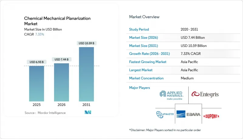
成長的驅動力來自FinFET電晶體向環柵(GAA)電晶體的過渡、3D整合技術的發展,以及碳化矽(SiC)和氮化鎵(GaN)在功率元件中日益廣泛的應用。代工廠持續擴大大規模能,美國和歐盟的政府獎勵也促進了本地化學機械拋光(CMP)供應鏈的發展。設備供應緊張限制了產能擴張,而永續性措施則加速了對低磨料和無磨料拋光液的需求。地緣政治出口限制正在重塑設備流通格局,並促進西方和中國供應商之間的平行創新交流。
全球化學機械拋光(CMP)市場趨勢與洞察
加速採用GAA和3D積體電路
環柵(GAA)電晶體引入了新型金屬柵堆疊結構,對化學機械拋光(CMP)製程提出了更高的選擇性去除率和更嚴格的缺陷閾值要求,從而改變了CMP製程的本質。各大晶圓代工廠正計畫量產3nm及以下GAA節點,這推動了配備先進終點控制功能的300mm單晶拋光機的設備更新換代。互補的3D整合技術,例如穿透矽通孔,需要在多個晶圓表面上實現超平整的銅層。因此,CMP平台整合了封閉回路型拋光墊調節和即時拋光液監控功能,以在更嚴格的公差範圍內保持產量比率。
SiC/GaN功率元件的快速成長
碳化矽和氮化鎵晶片具有高硬度和化學惰性,這顯著增加了拋光時間和耗材成本。採用鹼性化學成分和工程磨料的專用拋光液可達到接近 1µm/h 的去除率,同時將表面粗糙度保持在 0.05nm 以下。汽車電氣化正在加速對這些材料的需求,促使工具製造商推出耐磨損且能防止碳化矽生產線與傳統矽生產線交叉污染的拋光墊設計。
磨料投入成本飆升
當稀土元素供應緊張或化工廠進行檢修時,氧化鈰和過氧化氫等高純度原料的價格會飆升。據美國地質調查局稱,中國仍然是稀土元素進口的主要來源國,這使得全球漿料供應商容易受到貿易緊張局勢的影響。供應商正在透過調整漿料配方、降低磨料含量以及透過過濾回收廢液來應對這項挑戰。
細分市場分析
到2025年,設備將佔化學機械拋光(CMP)市場規模的62.78%。支出主要集中在單晶圓設備上,該設備可實現晶圓內亞奈米級不均勻性,並整合封閉回路型調諧功能以管理拋光墊表面狀況。預計到2031年,該細分市場將以7.54%的複合年成長率成長,這主要得益於晶圓廠採用支援GAA製程和寬能能隙的新基板。同時,清洗模組也在升級,以去除7奈米以下製程節點的奈米級缺陷。
耗材佔總收入的37.22%,其中以拋光液主導,其持續的需求確保了穩定的市場需求。二氧化矽基介電拋光液佔據主導地位,而一些小眾的氧化鈰配方則用於玻璃和藍寶石拋光。拋光墊供應商正在推出帶有溝槽的聚合物混合物,以保持穩定的去除率,並在更長的使用壽命內最大限度地減少缺陷的產生。不斷發展的永續性目標正在加速向低磨損性化學品的轉變,使得當性能和環境指標相符時,耗材供應商能夠獲得更高的價格。
區域分析
預計到2025年,亞太地區將佔全球營收的64.12%,並在2031年之前維持8.41%的複合年成長率。中國當地的本土化策略正推動晶圓廠建設的蓬勃發展,而台灣地區則繼續保持主導。韓國正在加大對高層數3D NAND和DRAM的投資,從而推動了對介電層和金屬平坦化產能的需求。日本供應商正利用其在超高純度化學品和精密焊盤領域數十年的專業經驗,進一步強化該地區垂直整合的生態系統。
北美地區營收排名第二。聯邦政府的激勵措施促進了新晶圓廠的建設,而由於客戶優先考慮供應鏈安全,國內設備製造商也獲得了大量訂單。亞利桑那州和紐約州的先進封裝計畫刺激了符合在地採購規定的CMP耗材的區域需求。對中國高階拋光墊出口的限制正在分割市場,並提升北美CMP供應商的戰略價值。
歐洲已設定目標,2030年實現全球半導體產量20%的目標,並將製造業的永續性放在首位。區域材料製造商正在擴大電子級過氧化氫和特殊漿料的產能,而德國和荷蘭的設備製造商則正在調整其化學機械拋光(CMP)產品,使其符合歐盟的環境指令。政府資助的異質整合試點生產線正在推動研究中心和專業代工廠逐步引入CMP設備。
其他福利:
- Excel格式的市場預測(ME)表
- 3個月的分析師支持
目錄
第1章 引言
- 研究假設和市場定義
- 調查範圍
第2章調查方法
第3章執行摘要
第4章 市場情勢
- 市場概覽
- 市場促進因素
- 加速採用GAA和3D積體電路
- SiC/GaN功率元件的快速成長
- 隨著微型化進程的推進,節點特定的CMP步驟數量減少。
- 人工智慧資料中心資本投資的漣漪效應(高階互連層)
- 美國和歐盟的晶圓廠激勵措施推動了CMP供應的在地化。
- 向低磨蝕性漿料的永續性推進
- 市場限制
- 漿料投入成本(稀土元素)突然增加
- 300mm刀具的OEM生產能力緊張。
- 不同材料化學機械加工中的交叉污染風險
- 美國和中國對高階衛生棉和護髮素的出口限制
- 價值/供應鏈分析
- 監管環境
- 技術展望
- 波特五力分析
- 新進入者的威脅
- 供應商的議價能力
- 買方的議價能力
- 替代品的威脅
- 競爭對手之間的競爭
- 投資分析
第5章 市場規模與成長預測
- 依產品類型
- CMP設備
- 單晶圓CMP系統
- CMP後處理清洗設備
- 批量CMP系統
- 其他
- CMP耗材
- CMP漿料
- 二氧化矽基漿料
- 氧化鋁基漿料
- 氧化鈰漿
- 複合材料/工程磨料漿料
- 其他材質(氧化鋯、鑽石等)
- 軟墊
- 其他耗材(過濾器、CMP後處理用清潔劑等)
- CMP漿料
- CMP設備
- 透過使用
- 積體電路
- 化合物半導體
- 微機電系統(MEMS)和奈米機電系統(NEMS)
- 先進包裝
- 其他用途
- 最終用戶
- 鑄造廠
- 整合裝置製造商(IDM)
- 半導體外包組裝和測試 (OSAT)
- 研發機構/大學
- 按地區
- 北美洲
- 美國
- 加拿大
- 墨西哥
- 歐洲
- 德國
- 法國
- 英國
- 義大利
- 其他歐洲地區
- 亞太地區
- 中國
- 日本
- 韓國
- 印度
- 亞太其他地區
- 南美洲
- 巴西
- 阿根廷
- 南美洲其他地區
- 中東
- 以色列
- 沙烏地阿拉伯
- 阿拉伯聯合大公國
- 其他中東地區
- 非洲
- 南非
- 埃及
- 其他非洲地區
- 北美洲
第6章 競爭情勢
- 市場集中度分析
- 策略趨勢與發展
- 供應商定位分析
- 公司簡介
- Applied Materials Inc.
- Entegris Inc.
- EBARA Corporation
- Lapmaster Wolters GmbH
- DuPont de Nemours, Inc.
- Fujimi Incorporated
- Revasum Inc.
- Resonac Holdings Corporation
- Okamoto Corporation
- FUJIFILM Corporation
- Tokyo Seimitsu Co., Ltd.
- Lam Research Corporation
- KLA Corporation
- Hitachi High-Tech Corporation
- Cabot Microelectronics Corporation
- 3M Company
- Saint-Gobain Surface Conditioning
- BASF SE
- Nagase ChemteX Corporation
- Ace Nanochem Co., Ltd.
第7章 市場機會與未來展望
Chemical mechanical planarization market size in 2026 is estimated at USD 7.44 billion, growing from 2025 value of USD 6.93 billion with 2031 projections showing USD 10.59 billion, growing at 7.33% CAGR over 2026-2031.
Growth is propelled by the transition from FinFET to gate-all-around (GAA) transistors, 3D-integration, and the rising use of silicon carbide (SiC) and gallium nitride (GaN) in power devices. Foundries continue large-scale capacity additions, and government incentives in the United States and European Union encourage local CMP supply chains. Tight tool availability constrains production ramps, while sustainability initiatives accelerate demand for low-abrasive and abrasive-free slurries. Geopolitical export controls reshape equipment flows and spur parallel innovation tracks between Western and Chinese vendors.
Global Chemical Mechanical Planarization Market Trends and Insights
Accelerating GAA and 3D-IC adoption
Gate-all-around transistors alter CMP chemistries by introducing new metal gate stacks that require highly selective removal rates and tighter defectivity thresholds. Leading foundries have scheduled volume production of GAA nodes below 3 nm, driving an equipment refresh cycle for 300 mm single-wafer polishers with advanced endpoint control. Complementary 3D-integration techniques, such as through-silicon vias, demand ultra-flat copper layers across multiple wafer surfaces. CMP platforms, therefore, integrate closed-loop pad conditioning and real-time slurry monitoring to sustain yields at ever-smaller tolerances .
Rapid growth in SiC/GaN power devices
Silicon carbide and gallium nitride wafers exhibit hardness and chemical inertness that multiply polish times and consumable costs. Dedicated slurries using alkaline chemistries and engineered abrasives now achieve removal rates near 1 µm/h while holding surface roughness below 0.05 nm. Automotive electrification accelerates demand for these materials, prompting tool makers to release pad designs resilient to abrasive wear and cross-contamination shielding between SiC and traditional silicon lines.
Escalating slurry input costs
Cerium oxide, hydrogen peroxide, and other high-purity inputs show price spikes when rare-earth supply tightens or chemical plants undergo maintenance. The U.S. Geological Survey notes China remains the main source of rare-earth imports, leaving global slurry vendors exposed to trade disputes . Vendors respond by reformulating slurries with lower abrasive loads and recycling spent solutions through filtration loops.
Other drivers and restraints analyzed in the detailed report include:
- AI datacenter capital expenditure
- U.S. and EU fab incentives
- Tight OEM capacity for 300 mm tools
For complete list of drivers and restraints, kindly check the Table Of Contents.
Segment Analysis
Equipment represented 62.78% of the chemical mechanical planarization market size in 2025. Spending concentrates on single-wafer tools that deliver within-wafer non-uniformity below 1 nm and integrate closed-loop conditioning for pad surface health. The segment is forecast to rise at a 7.54% CAGR to 2031 as fabs install new platforms that support GAA processes and wide-bandgap substrates. Cleaning modules undergo concurrent upgrades to remove nanoscale defects at sub-7 nm nodes.
Consumables account for 37.22% of revenue, led by slurries whose recurring nature ensures stable demand. Silica-based dielectric slurries dominate, while niche ceria formulas address glass and sapphire polishing. Pad suppliers release grooved polymer blends that sustain consistent removal rates and minimize defectivity over extended pad life. Sustainability goals accelerate the shift to low-abrasive chemistries, positioning consumables vendors for premium pricing when performance and environmental metrics converge.
The Chemical Mechanical Planarization Market Report is Segmented by Product Type (CMP Equipment, CMP Consumables), Application (Integrated Circuit, Compound Semiconductor, MEMS and NEMS, Advanced Packaging, Other Applications), End-User (Foundries, Idms, OSAT, R&D Institutes/Universities), and Geography (North America, Europe, Asia Pacific, Rest of World). The Market Forecasts are Provided in Terms of Value (USD).
Geography Analysis
Asia Pacific generated 64.12% of 2025 revenue and is projected to record an 8.41% CAGR through 2031. Mainland China's localization push prompts aggressive wafer-fab construction, while Taiwan retains leadership in cutting-edge logic and advanced packaging. South Korea invests in high-layer count 3D NAND and DRAM, boosting demand for dielectric and metal planarization capacity. Japanese suppliers leverage decades-long expertise in ultrapure chemicals and precision pads, reinforcing the region's vertically integrated ecosystem.
North America ranks second by revenue. Federal incentives have unlocked new fab commitments, and domestic equipment leaders capture significant orders as customers prioritize secure supply chains. Advanced packaging initiatives in Arizona and New York stimulate regional demand for CMP consumables that comply with local content rules. Export controls limit high-end pad shipments to China, creating a bifurcated market and heightening strategic value for North American CMP vendors.
Europe pursues 20% global semiconductor output by 2030, emphasizing manufacturing sustainability. Regional materials firms expand electronics-grade hydrogen peroxide and specialty slurry capacity, while equipment makers in Germany and the Netherlands align CMP offerings with EU environmental directives. Government funding supports pilot lines for heterogeneous integration, driving incremental CMP tool installations across research hubs and specialty foundries.
- Applied Materials Inc.
- Entegris Inc.
- EBARA Corporation
- Lapmaster Wolters GmbH
- DuPont de Nemours, Inc.
- Fujimi Incorporated
- Revasum Inc.
- Resonac Holdings Corporation
- Okamoto Corporation
- FUJIFILM Corporation
- Tokyo Seimitsu Co., Ltd.
- Lam Research Corporation
- KLA Corporation
- Hitachi High-Tech Corporation
- Cabot Microelectronics Corporation
- 3M Company
- Saint-Gobain Surface Conditioning
- BASF SE
- Nagase ChemteX Corporation
- Ace Nanochem Co., Ltd.
Additional Benefits:
- The market estimate (ME) sheet in Excel format
- 3 months of analyst support
TABLE OF CONTENTS
1 INTRODUCTION
- 1.1 Study Assumptions and Market Definition
- 1.2 Scope of the Study
2 RESEARCH METHODOLOGY
3 EXECUTIVE SUMMARY
4 MARKET LANDSCAPE
- 4.1 Market Overview
- 4.2 Market Drivers
- 4.2.1 Accelerating GAA and 3D-IC adoption
- 4.2.2 Rapid growth in SiC/GaN power devices
- 4.2.3 Shrinking node-specific CMP step count
- 4.2.4 AI datacenter capex pull-through (advanced interconnect layers)
- 4.2.5 U.S. and EU fab incentives localizing CMP supply
- 4.2.6 Sustainability push for low-abrasive slurries
- 4.3 Market Restraints
- 4.3.1 Escalating slurry input costs (rare earths)
- 4.3.2 Tight OEM capacity for 300 mm tools
- 4.3.3 Cross-contamination risk in hetero-material CMP
- 4.3.4 China-US export controls on high-end pads and conditioners
- 4.4 Value / Supply-Chain Analysis
- 4.5 Regulatory Landscape
- 4.6 Technological Outlook
- 4.7 Porter Five Forces Analysis
- 4.7.1 Threat of New Entrants
- 4.7.2 Bargaining Power of Suppliers
- 4.7.3 Bargaining Power of Buyers
- 4.7.4 Threat of Substitutes
- 4.7.5 Competitive Rivalry
- 4.8 Investment Analysis
5 MARKET SIZE AND GROWTH FORECASTS (VALUE)
- 5.1 By Product Type
- 5.1.1 CMP Equipment
- 5.1.1.1 Single-Wafer CMP Systems
- 5.1.1.2 Post-CMP Cleaning Equipment
- 5.1.1.3 Batch CMP Systems
- 5.1.1.4 Others
- 5.1.2 CMP Consumables
- 5.1.2.1 CMP Slurry
- 5.1.2.1.1 Silica-Based Slurry
- 5.1.2.1.2 Aluminum Oxide-Based Slurry
- 5.1.2.1.3 Cerium Oxide-Based Slurry
- 5.1.2.1.4 Composite/Engineered Abrasive Slurry
- 5.1.2.1.5 Other (Zirconia, Diamond, etc.)
- 5.1.2.2 Pads
- 5.1.2.3 Other Consumables (Filters, Post-CMP Clean Chemistries, etc.)
- 5.1.2.1 CMP Slurry
- 5.1.1 CMP Equipment
- 5.2 By Application
- 5.2.1 Integrated Circuit
- 5.2.2 Compound Semiconductor
- 5.2.3 MEMS and NEMS
- 5.2.4 Advanced Packaging
- 5.2.5 Other Applications
- 5.3 By End-User
- 5.3.1 Foundries
- 5.3.2 Integrated Device Manufacturers (IDMs)
- 5.3.3 Outsourced Semiconductor Assembly and Test (OSAT)
- 5.3.4 R&D Institutes / Universities
- 5.4 By Geography
- 5.4.1 North America
- 5.4.1.1 United States
- 5.4.1.2 Canada
- 5.4.1.3 Mexico
- 5.4.2 Europe
- 5.4.2.1 Germany
- 5.4.2.2 France
- 5.4.2.3 United Kingdom
- 5.4.2.4 Italy
- 5.4.2.5 Rest of Europe
- 5.4.3 Asia Pacific
- 5.4.3.1 China
- 5.4.3.2 Japan
- 5.4.3.3 South Korea
- 5.4.3.4 India
- 5.4.3.5 Rest of Asia Pacific
- 5.4.4 South America
- 5.4.4.1 Brazil
- 5.4.4.2 Argentina
- 5.4.4.3 Rest of South America
- 5.4.5 Middle East
- 5.4.5.1 Israel
- 5.4.5.2 Saudi Arabia
- 5.4.5.3 United Arab Emirates
- 5.4.5.4 Rest of Middle East
- 5.4.6 Africa
- 5.4.6.1 South Africa
- 5.4.6.2 Egypt
- 5.4.6.3 Rest of Africa
- 5.4.1 North America
6 COMPETITIVE LANDSCAPE
- 6.1 Market Concentration Analysis
- 6.2 Strategic Moves and Developments
- 6.3 Vendor Positioning Analysis
- 6.4 Company Profiles (includes Global level Overview, Market level overview, Core Segments, Financials as available, Strategic Information, Products and Services, and Recent Developments)
- 6.4.1 Applied Materials Inc.
- 6.4.2 Entegris Inc.
- 6.4.3 EBARA Corporation
- 6.4.4 Lapmaster Wolters GmbH
- 6.4.5 DuPont de Nemours, Inc.
- 6.4.6 Fujimi Incorporated
- 6.4.7 Revasum Inc.
- 6.4.8 Resonac Holdings Corporation
- 6.4.9 Okamoto Corporation
- 6.4.10 FUJIFILM Corporation
- 6.4.11 Tokyo Seimitsu Co., Ltd.
- 6.4.12 Lam Research Corporation
- 6.4.13 KLA Corporation
- 6.4.14 Hitachi High-Tech Corporation
- 6.4.15 Cabot Microelectronics Corporation
- 6.4.16 3M Company
- 6.4.17 Saint-Gobain Surface Conditioning
- 6.4.18 BASF SE
- 6.4.19 Nagase ChemteX Corporation
- 6.4.20 Ace Nanochem Co., Ltd.
7 MARKET OPPORTUNITIES AND FUTURE OUTLOOK
- 7.1 White-space and Unmet-Need Assessment
 全球化學機械拋光(CMP)市場規模、佔有率、趨勢和成長分析報告(2026-2034年)
 2026年全球化學機械拋光(CMP)漿料和拋光墊市場報告2026年全球化學機械拋光(CMP)市場報告化學機械拋光漿料市場-2026-2031年預測
 半導體用CMP材料市場:按類型、應用、通路和最終用戶分類-2026年至2032年全球預測晶圓CMP材料市場按產品類型、晶圓尺寸、顆粒尺寸、應用和最終用途產業分類-2026-2032年全球預測
 濕式工作台市場:按類型、應用和地區分類
 機械式和電子式引信:全球市場佔有率和排名、總銷售額和需求預測(2025-2031 年)化學機械平坦化市場按組件、晶圓尺寸和應用分類 - 全球預測 2025-2032
 全球半導體晶圓 CMP 固定環市場 - 市場佔有率和排名、總收入和需求預測(2025-2031 年)