


 |
市場調查報告書
商品編碼
1911314
碳化矽(SiC)晶圓:市場佔有率分析、產業趨勢與統計、成長預測(2026-2031)Silicon Carbide (SiC) Wafer - Market Share Analysis, Industry Trends & Statistics, Growth Forecasts (2026 - 2031) |
||||||
※ 本網頁內容可能與最新版本有所差異。詳細情況請與我們聯繫。
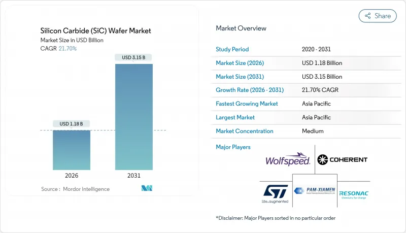
預計到 2026 年,碳化矽晶片市場價值將達到 11.8 億美元,從 2025 年的 9.7 億美元成長到 2031 年的 31.5 億美元,2026 年至 2031 年的複合年成長率為 21.7%。
這一成長軌跡得益於汽車產業向800V汽車平臺的轉型、工業電力電子領域對寬能能隙裝置日益成長的需求,以及政府為支持新建生產線而提供的激勵措施。晶體生長產量比率的穩定提升、8吋基板供應量的增加以及對高效快速充電基礎設施需求的不斷成長,正在推動市場進一步擴張。到2024年,亞太地區將佔據最大的市場佔有率,其垂直整合的生態系統將持續吸引上下游投資。儘管資本密集度仍然是關鍵的競爭因素,但那些掌握了缺陷減少、晶圓尺寸縮小和內部供應鏈管理技術的公司,將有望抓住碳化矽晶圓市場的下一波需求浪潮。碳化矽晶圓在高溫高頻工作環境下性能優於傳統矽晶圓。
全球碳化矽(SiC)晶圓市場趨勢及洞察
提高電動車滲透率並向 800V汽車平臺過渡
汽車製造商已透過特斯拉 Model S Plaid、現代 IONIQ 5 和起亞 EV6 等車款展示了大規模800V 系統的應用。雖然這些高壓架構顯著縮短了充電時間至 20 分鐘以內,但它們需要能夠承受高熱應力和電應力的功率 MOSFET。碳化矽滿足這些要求,其電場強度是矽的 10 倍,導熱係數是矽的 3 倍,從而推動了驅動逆變器和車載充電器對碳化矽的需求。雖然豪華車市場最初採用了這項技術,但晶圓成本的下降和供應鏈的成熟正在加速其在主流電動車平台上的應用,進一步提升了碳化矽晶圓市場作為下一代移動出行關鍵基礎技術的重要性。
800V充電基礎設施的快速擴張
為了最大限度地減少350kW充電站的轉換損耗,充電網路營運商選擇了碳化矽(SiC)作為晶圓材料。 Electrify Americas的主充電站整合了基於SiC的整流器和DC-DC模組,與矽相比,實現了更高的功率密度和更低的散熱。歐洲充電走廊供應商IONITY也採取了類似的策略,從而形成了一個良性循環的供需關係,促使汽車製造商採用800V平台。最終形成了一個涵蓋車輛、充電器和並聯型設備的生態系統,在提高晶圓需求的同時,透過提高能源效率降低成本,從而降低了網路營運商的整體擁有成本(TCO)。
200mm基板的供應限制
200毫米晶錠的生長週期通常超過200小時,且缺陷密度高於150毫米晶錠,這限制了汽車級基板的供應。產量比率下降推高了晶圓的平均售價(ASP),並減緩了設計到更大直徑的轉變。儘管製造商正在投資先進的原位監測技術和晶種最佳化以彌補缺口,但短期供不應求仍然抑制著碳化矽晶圓的市場出貨量成長,尤其是對於要求嚴格品質標準的汽車製造商。
細分市場分析
2025年,6吋晶圓佔據了碳化矽晶圓市場53.75%的佔有率。由於每片晶圓的裝置數量和晶粒折舊免稅額較高,這種傳統尺寸已成為大規模生產的標準。然而,預計到2031年,8吋晶圓的複合年成長率將達到28.6%,這進一步鞏固了其在牽引和光伏逆變器領域每安培成本的優勢。目前,8吋晶圓的資本支出仍然很高。一台用於200毫米晶體的高PVT爐造價為1500萬至2000萬美元,而6吋晶圓的PVT爐造價僅為800萬至1200萬美元。但是,8吋晶圓的晶粒產量可達6吋晶圓的2.2倍,隨著產量比率的提高,成本曲線將更加緊湊。隨著規模經濟效應的顯現,8吋基板碳化矽晶圓市場預計將成為日益重要的收入來源。
截至2024年,200毫米晶圓的產量比率比同等尺寸的6吋晶圓低15-20%,但最佳化加熱區設計與缺陷減少分析的投資已縮小了這一差距。汽車和可再生能源整合公司已啟動200毫米晶圓的認證項目,這預示著一旦大規模生產供應穩定,200毫米晶圓將被更廣泛地採用。隨著研發重心轉向高壓汽車或電網模組,小於4吋的晶圓尺寸持續下降,而大於12吋的原型產品仍僅限於學術界。因此,成功實現8吋晶圓的規模化生產標誌著碳化矽晶圓市場的關鍵轉折點。
到2025年,N型導電矽晶片將佔據碳化矽矽晶圓市場68.12%的佔有率。其低電阻率和穩定的摻雜分佈使其成為功率MOSFET、二極體和肖特基元件的關鍵材料。半絕緣基板傳統上是小眾市場,但預計到2031年將以23.6%的複合年成長率成長,這主要得益於5G基地台、雷達和衛星有效載荷中射頻和微波技術的應用。網路技術的進步和國防電子技術的發展需要高純度、電隔離的晶格結構來降低吉赫頻段的寄生電容,從而推動了半絕緣碳化矽矽晶圓市場的發展。
隨著晶圓直徑的增加,製造商不斷改進生長後退火和補償摻雜技術,以提高電阻率均勻性。航太和通訊公司由於其優異的熱處理性能,更傾向於使用半絕緣晶圓製造GaN-on-SiC HEMT裝置。因此,能夠確保高導熱性、電絕緣性和卓越射頻性能的晶圓在競爭格局中變得愈發重要。這一趨勢凸顯了半絕緣碳化矽在下一代裝置架構發展中將扮演的重要角色。
碳化矽 (SiC) 晶圓市場按晶圓直徑(小於 4 吋、大於 4 吋)、導電類型(N 型導電、半絕緣)、應用領域(電力電子、射頻元件等)、終端用戶產業(汽車及電動車、可再生能源及儲能等)、晶體生長技術(PVT、CVD 等)及地區進行細分。市場預測以美元以金額為準(USD) 為單位。
區域分析
北美位居第二,這得益於回流激勵政策和完善的電動車生態系統。 Wolfspeed位於莫霍克谷的晶圓廠開始量產200毫米晶圓,特斯拉檢驗了大規模碳化矽牽引逆變器,推動了區域供應協議的達成。安森美半導體決定投資高達20億美元在捷克共和國建造端到端的碳化矽生產系統,不僅為歐洲汽車製造商提供了更多選擇,也使其在美國保持了技術領先地位。同時,羅姆和SK Siltron透過生產高品質基板保持了技術優勢,使其能夠在價格下行壓力下維持高價位。
由於回流激勵政策和強大的電動車生態系統,北美保持了第二的位置。 Wolfspeed位於莫霍克谷的晶圓廠已開始量產200毫米晶圓,特斯拉大規模SiC牽引逆變器的檢驗促成了區域供應協議的達成。安森美半導體(ON Semiconductor)正在投資高達20億美元,在捷克共和國建造端到端的SiC生產能力,這不僅為歐洲汽車製造商提供了更多選擇,也保持了美國的技術優勢。
歐洲在綠色交易電氣化政策和強大的汽車產業基礎的推動下取得了長足進步。英飛凌擴大了在奧地利和德國的晶圓產能,以支援保時捷和奧迪的800V平台,並將品質和可靠性置於成本最低之上。意法半導體擴建了位於卡塔尼亞的工廠,為符合歐盟半導體自給自足目標的區域供應鏈奠定了基礎。碳化矽晶圓市場仍對價格敏感,但歐洲買家更重視汽車級可追溯性和嚴格的缺陷控制標準。
其他福利:
- Excel格式的市場預測(ME)表
- 3個月的分析師支持
目錄
第1章 引言
- 研究假設和市場定義
- 調查範圍
第2章調查方法
第3章執行摘要
第4章 市場情勢
- 市場概覽
- 市場促進因素
- 電動車日益普及以及向 800V汽車平臺的過渡
- 800V充電基礎設施快速發展
- 碳化矽在高溫和高頻性能方面優於矽
- 政府對寬能能隙晶圓廠的獎勵措施
- 中國垂直整合型碳化矽供應鏈的崛起
- 創新 200mm 體生長技術的進步可降低缺陷密度
- 市場限制
- 200mm基板供應限制
- 包裝引起的熱機械應力
- 資本密集型晶體生長設備
- 碳化矽切割廢棄物的回收利用問題
- 產業價值鏈分析
- 監管環境
- 技術展望
- 宏觀經濟因素的影響
- 波特五力分析
- 供應商的議價能力
- 買方的議價能力
- 新進入者的威脅
- 替代品的威脅
- 競爭對手之間的競爭
第5章 市場規模與成長預測
- 依晶圓直徑
- 小於4英寸
- 6吋
- 8吋
- 12吋或以上
- 依導電類型
- N型導電性
- 半絕緣
- 透過使用
- 電力電子
- 高頻裝置
- 光電子學和發光二極體
- 其他用途
- 按最終用途行業分類
- 汽車和電動車
- 可再生能源和儲能
- 電訊
- 工業馬達驅動裝置和不斷電系統(UPS)
- 航太/國防
- 其他終端用戶產業
- 透過晶體生長技術
- 物理蒸氣傳輸(PVT)
- 化學氣相沉積(CVD)
- 改良的萊利昇華法
- 其他技術
- 按地區
- 北美洲
- 美國
- 加拿大
- 南美洲
- 巴西
- 阿根廷
- 南美洲其他地區
- 歐洲
- 德國
- 法國
- 英國
- 義大利
- 西班牙
- 其他歐洲地區
- 亞太地區
- 中國
- 日本
- 韓國
- 台灣
- 印度
- 亞太其他地區
- 中東和非洲
- 中東
- 沙烏地阿拉伯
- 阿拉伯聯合大公國
- 其他中東地區
- 非洲
- 南非
- 奈及利亞
- 其他非洲地區
- 中東
- 北美洲
第6章 競爭情勢
- 市場集中度
- 策略趨勢
- 市佔率分析
- 公司簡介
- Wolfspeed Inc.
- Coherent Corp.
- Xiamen Powerway Advanced Material Co., Ltd.
- STMicroelectronics NV
- Resonac Holdings Corporation
- Atecom Technology Co., Ltd.
- SK Siltron Co., Ltd.
- SiCrystal GmbH
- Tankeblue Semiconductor Co., Ltd.
- Semiconductor Wafer Inc.
- GlobalWafers Co., Ltd.
- Sanan Optoelectronics Co., Ltd.
- ROHM Co., Ltd.
- Infineon Technologies AG
- onsemi Corporation
- Mitsubishi Electric Corporation
- Hebei Synlight Crystal Co., Ltd.
- Guangdong TySiC Semiconductor Co., Ltd.
- EpiWorld International Co., Ltd.
- Hench Semiconductor Co., Ltd.
- TYSTC Semiconductor Co., Ltd.
- ProChip Moissic Technologies Inc.
- Dow Silicon Carbide LLC
- Fraunhofer IISB(SiC Foundry)
- Nippon Steel & Sumitomo Metal SiC Materials Co., Ltd.
- LPE SpA
第7章 市場機會與未來展望
The silicon carbide wafer market size in 2026 is estimated at USD 1.18 billion, growing from 2025 value of USD 0.97 billion with 2031 projections showing USD 3.15 billion, growing at 21.7% CAGR over 2026-2031.
The growth trajectory is supported by the automotive industry's migration to 800 V vehicle platforms, wide-band-gap adoption in industrial power electronics, and government incentives that underwrite new fabrication lines. Steadily improving crystal-growth yields, wider availability of 8-inch substrates, and rising demand for efficient fast-charging infrastructure further underpin expansion. Asia-Pacific held the largest regional share in 2024, and its vertically integrated ecosystem continues to attract upstream and downstream investments. Capital intensity remains a key competitive filter, yet companies that master defect reduction, wafer scaling, and internal supply chains are positioned to capture the next wave of demand as the silicon carbide wafer market outperforms conventional silicon in high-temperature and high-frequency operating environments.
Global Silicon Carbide (SiC) Wafer Market Trends and Insights
Rising EV Penetration and Shift Toward 800 V Vehicle Platforms
Automakers demonstrated large-scale 800 V system adoption through models such as Tesla's Model S Plaid, Hyundai's IONIQ 5, and Kia's EV6. These high-voltage architectures reduced charging times well below 20 minutes yet demanded power MOSFETs capable of withstanding elevated thermal and electrical stress. Silicon carbide meets these thresholds due to a ten-fold higher critical electric field and three-fold higher thermal conductivity than silicon, which magnifies demand in traction inverters and onboard chargers. Luxury and premium segments adopted the technology first, but falling wafer costs and maturing supply chains now accelerate diffusion into mainstream EV platforms, reinforcing the silicon carbide wafer market as an essential enabler of next-generation mobility.
Rapid Build-out of 800 V Charging Infrastructure
Charging network operators selected silicon carbide to minimise conversion losses in 350 kW stations. Electrify America's flagship sites integrated SiC-based rectifiers and DC-DC modules, achieving higher power density and lower heat dissipation compared with silicon. European corridor provider IONITY followed a similar path, creating a supply-demand flywheel that encourages automakers to embrace 800 V platforms. The resulting ecosystem, spanning vehicles, chargers, and grid-interfacing equipment, ramps up wafer volumes while compressing total ownership cost for network operators through energy-efficiency savings.
Limited Availability of 200 mm Substrates
Crystal-growth cycles for 200 mm boules often exceeded 200 hours and yielded higher defect densities than 150 mm equivalents, constraining the supply of automotive-grade substrates. Yield penalties elevated wafer ASPs and delayed design transitions to larger diameters. Fabricators invested in advanced in-situ monitoring and seed-crystal optimisation to close the gap, yet near-term shortages continue to cap silicon carbide wafer market shipment growth, especially for carmakers that require stringent quality thresholds.
Other drivers and restraints analyzed in the detailed report include:
- High-Temperature, High-Frequency Performance Advantages over Silicon
- Government Incentives for Wide-Band-Gap Fabs
- Packaging-Induced Thermo-Mechanical Stress
For complete list of drivers and restraints, kindly check the Table Of Contents.
Segment Analysis
The silicon carbide wafer market recorded 6-inch substrates at 53.75% share in 2025. Device counts per wafer and depreciation per die positioned this legacy diameter as the volume benchmark. However, 8-inch substrates are forecast to expand at a 28.6% CAGR through 2031, underscoring the cost-per-ampere advantage for traction inverters and PV inverters. Equipment investments remain high-PVT furnaces for 200 mm crystals cost USD 15-20 million versus USD 8-12 million for 6-inch. Nonetheless, each 8-inch wafer can deliver up to a 2.2-fold increase in die output, tightening the cost curve as yields improve. The silicon carbide wafer market size for 8-inch substrates is projected to command an increasingly large revenue pool as scale economies kick in.
Although yield rates lagged 6-inch equivalents by 15-20% in 2024, investment in hot-zone design optimisation and defect-reduction analytics narrowed the gap. Automotive and renewable energy integrators began qualification programs for 200 mm die, signalling broader acceptance once volume supply stabilises. less than 4-inch formats continued to decline as R&D moves toward high-voltage automotive or grid modules, while above 12-inch prototypes remained confined to academia. Successful scale-up to 8-inch thus stands as the pivotal inflection point for the silicon carbide wafer market.
N-type conductive wafers accounted for 68.12% of the silicon carbide wafer market share in 2025. Their low resistivity and stable dopant profiles made them indispensable for power MOSFETs, diodes, and Schottky devices. Semi-insulating substrates, although historically niche, are poised for 23.6% CAGR growth to 2031, driven by RF and microwave adoption in 5G base stations, radar, and satellite payloads. The silicon carbide wafer market size allocated to semi-insulating material is set to swell as network densification and defense electronics demand pure, electrically isolated lattices to limit parasitic capacitance at gigahertz frequencies.
Producers continue to refine post-growth annealing and compensation-doping techniques to lift resistivity uniformity across larger diameters. Aerospace and telecommunications firms favour semi-insulating wafers for GaN-on-SiC HEMTs that deliver superior thermal handling. As a result, the competitive landscape increasingly values substrates that ensure high thermal conductivity, electrical isolation, and superior RF performance. This trend highlights semi-insulating silicon carbide as a pivotal player in the evolution of next-generation device architectures.
Silicon Carbide (SiC) Wafer Market is Segmented by Wafer Diameter (less Than 4 Inch, and More), Conductivity Type (N-Type Conductive and Semi-Insulating), Application (Power Electronics, RF Devices, and More), End-Use Industry (Automotive and Electric Vehicles, Renewable Energy and Storage, and More), Crystal-Growth Technology (PVT, CVD, and More), and Geography. The Market Forecasts are Provided in Terms of Value (USD).
Geography Analysis
North America ranked second, bolstered by reshoring incentives and a deep EV ecosystem. Wolfspeed's Mohawk Valley fab ramped 200 mm wafers, and Tesla validated large-scale SiC traction inverters, spurring regional supply agreements. OnSemi committed up to USD 2 billion to establish end-to-end SiC production in the Czech Republic, providing optionality for European auto OEMs while retaining US technology leadership.chnology leadership through premium substrate production at ROHM and SK Siltron, preserving high ASPs despite down-price pressure.
North America ranked second, bolstered by reshoring incentives and a deep EV ecosystem. Wolfspeed's Mohawk Valley fab ramped 200 mm wafers, and Tesla validated large-scale SiC traction inverters, spurring regional supply agreements. OnSemi committed up to USD2 billion to establish end-to-end SiC production in the Czech Republic, providing optionality for European auto OEMs while retaining US technology leadership.
Europe advanced on the back of Green Deal electrification policies and a strong automotive base. Infineon expanded wafer output in Austria and Germany to serve Porsche and Audi 800 V platforms, emphasising quality and reliability over lowest cost. STMicroelectronics scaled its Catania site, anchoring a local supply chain that aligned with EU semiconductor sovereignty goals. Although the silicon carbide wafer market remained price sensitive, European buyers valued automotive-grade traceability and tight defect specifications.
- Wolfspeed Inc.
- Coherent Corp.
- Xiamen Powerway Advanced Material Co., Ltd.
- STMicroelectronics N.V.
- Resonac Holdings Corporation
- Atecom Technology Co., Ltd.
- SK Siltron Co., Ltd.
- SiCrystal GmbH
- Tankeblue Semiconductor Co., Ltd.
- Semiconductor Wafer Inc.
- GlobalWafers Co., Ltd.
- Sanan Optoelectronics Co., Ltd.
- ROHM Co., Ltd.
- Infineon Technologies AG
- onsemi Corporation
- Mitsubishi Electric Corporation
- Hebei Synlight Crystal Co., Ltd.
- Guangdong TySiC Semiconductor Co., Ltd.
- EpiWorld International Co., Ltd.
- Hench Semiconductor Co., Ltd.
- TYSTC Semiconductor Co., Ltd.
- ProChip Moissic Technologies Inc.
- Dow Silicon Carbide LLC
- Fraunhofer IISB (SiC Foundry)
- Nippon Steel & Sumitomo Metal SiC Materials Co., Ltd.
- LPE S.p.A.
Additional Benefits:
- The market estimate (ME) sheet in Excel format
- 3 months of analyst support
TABLE OF CONTENTS
1 INTRODUCTION
- 1.1 Study Assumptions and Market Definition
- 1.2 Scope of the Study
2 RESEARCH METHODOLOGY
3 EXECUTIVE SUMMARY
4 MARKET LANDSCAPE
- 4.1 Market Overview
- 4.2 Market Drivers
- 4.2.1 Rising EV penetration and shift toward 800-V vehicle platforms
- 4.2.2 Rapid build-out of 800 V charging infrastructure
- 4.2.3 High-temperature, high-frequency performance advantages over Si
- 4.2.4 Government incentives for wide-band-gap fabs
- 4.2.5 Emergence of vertically-integrated SiC supply chains in China
- 4.2.6 Novel 200 mm bulk-growth breakthroughs lowering defect density
- 4.3 Market Restraints
- 4.3.1 Limited availability of 200 mm substrates
- 4.3.2 Packaging-induced thermo-mechanical stress
- 4.3.3 Capital-intensive crystal-growth equipment
- 4.3.4 Recycling challenges for SiC kerf waste
- 4.4 Industry Value Chain Analysis
- 4.5 Regulatory Landscape
- 4.6 Technological Outlook
- 4.7 Impact of Macroeconomic Factors
- 4.8 Porter's Five Forces Analysis
- 4.8.1 Bargaining Power of Suppliers
- 4.8.2 Bargaining Power of Buyers
- 4.8.3 Threat of New Entrants
- 4.8.4 Threat of Substitutes
- 4.8.5 Intensity of Competitive Rivalry
5 MARKET SIZE AND GROWTH FORECASTS (VALUE)
- 5.1 By Wafer Diameter
- 5.1.1 less than 4 inch
- 5.1.2 6 inch
- 5.1.3 8 inch
- 5.1.4 above 12 inch
- 5.2 By Conductivity Type
- 5.2.1 N-Type Conductive
- 5.2.2 Semi-insulating
- 5.3 By Application
- 5.3.1 Power Electronics
- 5.3.2 Radio-Frequency Devices
- 5.3.3 Optoelectronics and LED
- 5.3.4 Other Applications
- 5.4 By End-use Industry
- 5.4.1 Automotive and Electric Vehicles
- 5.4.2 Renewable Energy and Storage
- 5.4.3 Telecommunications
- 5.4.4 Industrial Motor Drives and UPS
- 5.4.5 Aerospace and Defense
- 5.4.6 Other End-user Industries
- 5.5 By Crystal-Growth Technology
- 5.5.1 Physical Vapor Transport (PVT)
- 5.5.2 Chemical Vapor Deposition (CVD)
- 5.5.3 Modified Lely Sublimation
- 5.5.4 Other Technologies
- 5.6 By Geography
- 5.6.1 North America
- 5.6.1.1 United States
- 5.6.1.2 Canada
- 5.6.2 South America
- 5.6.2.1 Brazil
- 5.6.2.2 Argentina
- 5.6.2.3 Rest of South America
- 5.6.3 Europe
- 5.6.3.1 Germany
- 5.6.3.2 France
- 5.6.3.3 United Kingdom
- 5.6.3.4 Italy
- 5.6.3.5 Spain
- 5.6.3.6 Rest of Europe
- 5.6.4 Asia-Pacific
- 5.6.4.1 China
- 5.6.4.2 Japan
- 5.6.4.3 South Korea
- 5.6.4.4 Taiwan
- 5.6.4.5 India
- 5.6.4.6 Rest of Asia-Pacific
- 5.6.5 Middle East and Africa
- 5.6.5.1 Middle East
- 5.6.5.1.1 Saudi Arabia
- 5.6.5.1.2 United Arab Emirates
- 5.6.5.1.3 Rest of Middle East
- 5.6.5.2 Africa
- 5.6.5.2.1 South Africa
- 5.6.5.2.2 Nigeria
- 5.6.5.2.3 Rest of Africa
- 5.6.5.1 Middle East
- 5.6.1 North America
6 COMPETITIVE LANDSCAPE
- 6.1 Market Concentration
- 6.2 Strategic Moves
- 6.3 Market Share Analysis
- 6.4 Company Profiles (includes Global level Overview, Market level overview, Core Segments, Financials as available, Strategic Information, Market Rank/Share for key companies, Products and Services, and Recent Developments)
- 6.4.1 Wolfspeed Inc.
- 6.4.2 Coherent Corp.
- 6.4.3 Xiamen Powerway Advanced Material Co., Ltd.
- 6.4.4 STMicroelectronics N.V.
- 6.4.5 Resonac Holdings Corporation
- 6.4.6 Atecom Technology Co., Ltd.
- 6.4.7 SK Siltron Co., Ltd.
- 6.4.8 SiCrystal GmbH
- 6.4.9 Tankeblue Semiconductor Co., Ltd.
- 6.4.10 Semiconductor Wafer Inc.
- 6.4.11 GlobalWafers Co., Ltd.
- 6.4.12 Sanan Optoelectronics Co., Ltd.
- 6.4.13 ROHM Co., Ltd.
- 6.4.14 Infineon Technologies AG
- 6.4.15 onsemi Corporation
- 6.4.16 Mitsubishi Electric Corporation
- 6.4.17 Hebei Synlight Crystal Co., Ltd.
- 6.4.18 Guangdong TySiC Semiconductor Co., Ltd.
- 6.4.19 EpiWorld International Co., Ltd.
- 6.4.20 Hench Semiconductor Co., Ltd.
- 6.4.21 TYSTC Semiconductor Co., Ltd.
- 6.4.22 ProChip Moissic Technologies Inc.
- 6.4.23 Dow Silicon Carbide LLC
- 6.4.24 Fraunhofer IISB (SiC Foundry)
- 6.4.25 Nippon Steel & Sumitomo Metal SiC Materials Co., Ltd.
- 6.4.26 LPE S.p.A.
7 MARKET OPPORTUNITIES AND FUTURE OUTLOOK
- 7.1 White-space and Unmet-need Assessment
 全球碳化矽晶圓拋光市場規模、佔有率、趨勢和成長分析報告(2026-2034年)
 2026年全球碳化矽晶圓加工市場研究報告
 4吋SiC晶圓市場依產品類型、電壓等級、純度等級及應用分類,全球預測(2026-2032年)4吋和6吋SiC晶圓市場(按晶圓尺寸、晶體結構、摻雜類型、裝置類型、通路和應用分類)-全球預測,2026-2032年6吋導電SiC晶圓市場(按應用、終端用戶產業、多型、基板類型、外延層和摻雜類型分類),全球預測,2026-2032年8吋碳化矽晶圓市場(依晶圓類型、元件類型、摻雜類型、電阻率、表面光潔度和應用分類),全球預測,2026-2032年碳化矽晶圓市場按產品類型、晶圓直徑、應用、通路和裝置類型分類,全球預測(2026-2032年)碳化矽(SiC)晶圓和基板市場(按多型、晶圓直徑、晶圓取向、晶圓類型和應用分類),全球預測,2026-2032年
 碳化矽晶片:全球市佔率及排名、總收入及需求預測(2025-2031年)碳化矽拋光耗材:全球市佔率排名、總銷售額及需求預測(2025-2031年)