


 |
市場調查報告書
商品編碼
1910440
電子設計自動化工具(EDA):市場佔有率分析、產業趨勢與統計、成長預測(2026-2031)Electronic Design Automation Tools (EDA) - Market Share Analysis, Industry Trends & Statistics, Growth Forecasts (2026 - 2031) |
||||||
※ 本網頁內容可能與最新版本有所差異。詳細情況請與我們聯繫。
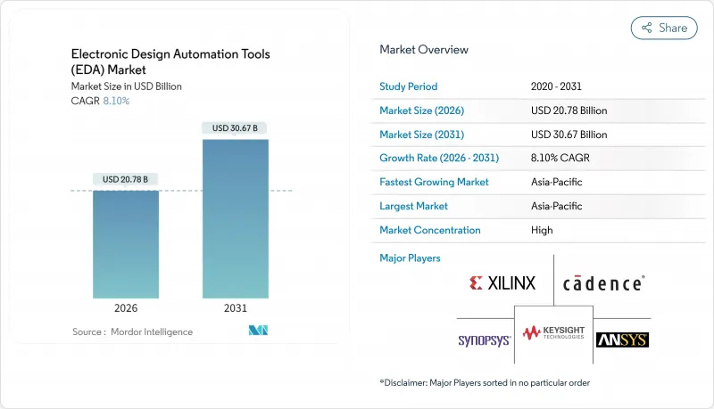
預計到 2026 年,電子設計自動化 (EDA) 工具市場規模將達到 207.8 億美元,高於 2025 年的 192.2 億美元。
預計到 2031 年將達到 306.7 億美元,2026 年至 2031 年的複合年成長率為 8.1%。
這一前景基於電晶體尺寸的加速縮小、人工智慧驅動的設計流程以及晶圓代工廠與設計工具之間日益密切的合作。晶片設計人員正從手動規則調整轉向數據驅動的最佳化,從而縮短流片週期並降低返工風險。雲端容量的激增正在擴大先進檢驗技術的使用範圍,而汽車功能安全法規則推動形式化方法進入主流設計領域。 Synopsys 以 350 億美元收購 Ansys 的交易預計將於 2025 年完成,這標誌著設計領域正系統性地轉向整合裝置系統平台,該平台能夠同時最佳化晶片、封裝和系統的效能。同時,地緣政治出口限制正在催生並行的 EDA 生態系統,迫使供應商為多個地區的晶圓代工廠認證流程,以避免收入損失。
全球電子設計自動化工具 (EDA) 市場趨勢與洞察
先進節點晶片密度快速提升
與7nm製程相比,全環柵(GAA)電晶體、背面供電技術和多晶片封裝使設計規則檢查(DRC)的數量增加了10倍。目前,晶圓代工廠正與EDA領導企業合作開發相關流程,Synopsys和台積電已於2025年4月完成了A16和N2P節點完整數位和類比工具鏈的認證。統一的探索到最終確認流程可減少代價高昂的重新設計,在3nm製程下,每次重新設計的成本可能超過5000萬美元。英特爾的18A計畫也同樣依賴整合流程,用於將運算、記憶體和I/O整合在單一基板上的2.5D/3D架構。
人工智慧/機器學習加速器和客製化SoC的興起
超大規模和邊緣運算提供者正在加速採用專用推理晶片。 Cadence 報告稱,其 2025 年第一季半導體 IP 營收年增 40%,並將這一成長歸功於人工智慧和晶片組計劃。 NVIDIA、ASML、台積電和 Synopsys 的 CuLitho 軟體堆疊將微影術模擬速度提高了 40 倍,從而能夠實現滿足人工智慧能效目標的光罩版圖佈局。隨著加速器異質性的增加,SIP 的重用和封裝內互連標準的標準化正在推動對 IP檢驗的需求。
主要EDA套件的授權成本不斷上漲
用於全面3nm製程簽核的企業級年度套餐價格現已超過每席100萬美元,迫使中型晶圓廠優先考慮工具模組並延長更新周期。寡占的供應結構維持了供應商的定價權,尤其是在時序收斂和微影術軟體包領域,因為目前尚無開放原始碼替代方案。
細分市場分析
半導體智慧財產權(SIP)預計將以9.7%的複合年成長率在所有工具類別中位居榜首,這主要得益於晶片組架構的興起,此類架構需要檢驗的介面模組和混合訊號核心。到2025年,SIP將佔電子設計自動化(EDA)市場收入的18.74%,隨著晶圓代工廠推行「已知良品晶粒」策略,每個計劃的SIP附加率將比2023年翻倍。受單片SoC向異構封裝過渡的推動,SIP應用的EDA市場規模預計將在2031年之前顯著成長。
由於佈局佈線、靜態時序和 DRC 在整個流片過程中至關重要,IC 物理設計和檢驗部分保持了 35.82% 的佔有率,但透過 AI 增強的佈局規劃實現的多目標最佳化自動化,已將最近的 3nm 設計的周轉時間縮短了 30%。
前端設計工具的複合年成長率 (CAGR) 為 9.35%,這主要得益於高級綜合 (HLS) 和自然語言到 RTL 生成工具等生產力提昇技術的進步。預計到 2031 年,RTL 自動化領域的電子設計自動化 (EDA) 市場規模將顯著成長,這主要得益於人工智慧輔助程式碼產生技術能夠以更少的迭代次數捕捉功能意圖。佈局、佈線和時序收斂仍然佔據電子設計自動化 (EDA) 市場佔有率的 32.10%,這反映了簽核級時序收斂和高級 3D 寄生參數提取技術的不可替代性。
目前,生成式設計平台產生的佈局指導與手動編寫的腳本相比,可將導線長度減少 11%,漏電流減少 9%。然而,最終的系統單晶片 (SoC) 交付仍然需要代工廠核准的認證時序和電氣規則報告,這凸顯了成熟的後端工具鏈的重要性。
電子設計自動化工具 (EDA) 報告按工具類型(例如,電腦輔助設計、積體電路實體設計與檢驗)、設計流程階段(例如,前端設計 RTL)、部署模式(例如,本地部署、雲端部署)、最終用戶產業(例如,通訊基礎設施、家用電子電器)和地區(例如,北美)進行細分。市場預測以美元計價。
區域分析
亞太地區將在2025年佔據42.05%的市場佔有率,並在2031年之前以9.55%的複合年成長率成長。台灣和韓國的晶圓代工廠群聚將支撐區域工具需求,而中國正加速建造其自主研發的EDA堆疊,以應對美國的出口限制。政府主導的措施正在為人工智慧輔助的佈局佈線引擎和SPICE模擬器提供補貼,旨在3nm製程量產前實現流程在地化。憑藉印度豐富的工程人才資源,當地設計服務公司在2024年成長了17%,以滿足西方客戶對具成本效益RTL和DFT支援的需求。
北美憑藉主導,保持著其影響力。儘管該地區的市佔率將在2025年略微下降至29.15%,但它仍然是先進節點參考工具流程的主要來源。出口管制制度要求供應商對許可證金鑰實施地理圍欄,這增加了合規成本,並鎖定了北美的智慧財產權鏈。英特爾晶圓代工和新思科技在18A認證流程的合作,加強了美國重奪先進製造業市場佔有率的努力。歐洲正專注於汽車和工業應用,ISO 26262標準正在推動高階檢驗工具的普及。台積電計畫於2025年在慕尼黑開設設計中心,旨在將晶圓代工廠工程師融入區域供應鏈,並為3DIC封裝和低功耗人工智慧加速器提供直接支援。歐盟晶片津貼將優先為電子設計叢集提供研發稅額扣抵,進一步刺激區域電子設計自動化(EDA)技術的應用。中東、非洲和南美洲仍然是發展中地區,但在政府主導的晶圓製造計劃和物聯網部署取得進展的地區,這些地區正呈現兩位數的成長。
其他福利:
- Excel格式的市場預測(ME)表
- 3個月的分析師支持
目錄
第1章 引言
- 研究假設和市場定義
- 調查範圍
第2章調查方法
第3章執行摘要
第4章 市場情勢
- 市場概覽
- 市場促進因素
- 先進節點晶片密度快速提升
- 人工智慧/機器學習加速器和客製化SoC的普及
- 雲端原生EDA工作流程(EDA即服務)的興起
- 汽車產業 ISO 26262 功能安全標準合規性要求
- 開放原始碼硬體的普及正在推動檢驗的需求。
- 美國出口管制政策的兩極化加速了國內設計流程的發展。
- 市場限制
- 主要EDA套件的授權成本不斷上漲
- 5奈米及以下製程的物理設計工程師短缺
- 雲端採用過程中知識產權侵權和網路入侵的風險
- 莫耳定律的延伸速度比預期慢
- 價值鏈分析
- 監管環境
- 技術展望
- 波特五力分析
- 供應商的議價能力
- 買方的議價能力
- 新進入者的威脅
- 替代品的威脅
- 競爭對手之間的競爭
- 投資分析
- 宏觀經濟因素如何影響市場
第5章 市場規模與成長預測
- 按工具類型
- 電腦輔助工程(CAE)
- 積體電路物理設計與檢驗
- 印刷基板(PCB)和多晶片模組(MCM)
- 半導體智慧財產權(SIP)
- 服務
- 按階段設計流程
- 前端設計(RTL)
- 邏輯綜合和功能檢驗
- 佈局、佈線和時序收斂
- 最終核准(DFM、電源、SI、散熱設計)
- 透過部署模式
- 本地部署
- 基於雲端的
- 按最終用戶行業分類
- 通訊基礎設施
- 家用電子電器
- 汽車與出行
- 工業和能源
- 航太/國防
- 醫療設備
- 其他行業
- 按地區
- 北美洲
- 美國
- 加拿大
- 墨西哥
- 南美洲
- 巴西
- 阿根廷
- 南美洲其他地區
- 歐洲
- 德國
- 英國
- 法國
- 義大利
- 其他歐洲地區
- 亞太地區
- 中國
- 日本
- 韓國
- 印度
- 亞太其他地區
- 中東
- 沙烏地阿拉伯
- 阿拉伯聯合大公國
- 其他中東地區
- 非洲
- 南非
- 其他非洲地區
- 北美洲
第6章 競爭情勢
- 市場集中度
- 策略趨勢
- 市佔率分析
- 公司簡介
- Ansys Inc.
- Cadence Design Systems Inc.
- Synopsys Inc.
- Siemens Digital Industries Software(Mentor Graphics)
- Keysight Technologies Inc.
- Altium Limited
- Zuken Ltd.
- Xilinx Inc.(AMD Adaptive and Embedded Computing Group)
- Aldec Inc.
- Agnisys Inc.
- Lauterbach GmbH
- Silvaco Inc.
- Real Intent Inc.
- Axiomise Ltd.
- Imperas Software Ltd.
- PDF Solutions Inc.
- Flex Logix Technologies Inc.
- Andes Technology Corp.
- Cobham Gaisler AB
- Arteris Inc.
第7章 市場機會與未來展望
Electronic Design Automation Tools market size in 2026 is estimated at USD 20.78 billion, growing from 2025 value of USD 19.22 billion with 2031 projections showing USD 30.67 billion, growing at 8.1% CAGR over 2026-2031.
The outlook builds on faster transistor scaling, AI-enabled design flows, and closer foundry-tool collaboration. Chip architects are shifting from manual rule tuning to data-driven optimization that shortens tape-out cycles and lowers re-spin risk. Cloud-based capacity bursting is widening access to advanced verification, while automotive functional-safety mandates push formal methods into mainstream design. The 2025 completion of Synopsys' USD 35 billion acquisition of Ansys signals a systemic move toward unified device-to-system platforms able to co-optimize silicon, package, and full-system performance simultaneously. Meanwhile, geopolitical export controls spur parallel EDA ecosystems, compelling vendors to certify flows for multiple regional foundries to avoid revenue erosion.
Global Electronic Design Automation Tools (EDA) Market Trends and Insights
Soaring Chip-Density in Advanced Nodes
Gate-All-Around transistors, backside power delivery, and multi-die packaging produce a ten-fold rise in design-rule checks compared with 7 nm processes. Foundries now co-develop flows with EDA leaders; Synopsys and TSMC certified full digital and analog toolchains for A16 and N2P nodes in April 2025. Unified exploration-to-signoff environments reduce costly re-spins-each exceeding USD 50 million at 3 nm. Intel's 18A program likewise relies on integrated flows for 2.5D/3D architectures that merge compute, memory, and I/O on a single substrate.
Proliferation of AI/ML Accelerators and Custom SoCs
Hyperscale and edge providers increasingly commission purpose-built inference silicon. Cadence posted 40% YoY growth in semiconductor IP revenue in Q1 2025, attributing momentum to AI and chiplet projects. NVIDIA, ASML, TSMC, and Synopsys reported 40X lithography simulation speed-ups through the CuLitho software stack, enabling reticle layouts that meet AI power-per-watt targets. As accelerator heterogeneity rises, SIP reuse and on-package interconnect standards intensify demand for IP verification.
Escalating Licensing Costs for Leading EDA Suites
Annual enterprise bundles for comprehensive 3 nm sign-off now exceed USD 1 million per seat, forcing mid-tier fabs to prioritize tool modules and extend refresh cycles. Oligopolistic supply means price leverage remains with vendors, particularly for timing closure and lithography simulation packages that have no open-source substitute.
Other drivers and restraints analyzed in the detailed report include:
- Rise of Cloud-Native EDA Workflows (EDA-as-a-Service)
- Automotive ISO 26262 Functional-Safety Compliance Needs
- Talent Shortage in Sub-5 nm Physical-Design Engineers
For complete list of drivers and restraints, kindly check the Table Of Contents.
Segment Analysis
Semiconductor Intellectual Property (SIP) posted a 9.7% CAGR forecast, the fastest among tool categories, owing to rising chiplet architectures that favor verified interface blocks and mixed-signal cores. In 2025, SIP accounted for 18.74% of the Electronic Design Automation Tools market revenue, yet its attach rate per project has doubled since 2023 as foundries promote known-good-die strategies. The Electronic Design Automation Tools market size for SIP applications is projected to grow at a significant rate by 2031, underscoring the shift from monolithic SoCs to heterogeneous assembly.
IC Physical Design and Verification retained a 35.82% share thanks to the mandatory nature of placement, routing, static-timing, and DRC in every tape-out. However, AI-enhanced floorplanning automates multi-objective optimization, shrinking turnaround time by 30% on recent 3 nm designs.
Front-End Design tools record a 9.35% CAGR as high-level synthesis (HLS) and natural-language-to-RTL generators improve productivity. The Electronic Design Automation Tools market size for RTL automation is projected to grow significantly by 2031 on the back of AI-assisted code generation that captures functional intent in fewer iterations. Layout, Routing, and Timing Closure still governs 32.10% of the Electronic Design Automation Tools market share, reflecting the irreplaceable nature of sign-off-caliber timing convergence and advanced 3D parasitic extraction.
Generative design platforms now produce placement guidance that reduces wire length by 11% and leakage by 9% versus human scripts. Yet final SOC hand-off still relies on certified timing and electrical-rule reports accepted by foundries, cementing the relevance of established back-end toolchains.
The Electronic Design Automation Tools Report is Segmented by Tool Type (Computer-Aided Engineering, IC Physical Design and Verification, and More), Design-Flow Stage (Front-End Design RTL, and More), Deployment Mode (On-Premise, and Cloud-Based), End-User Industry (Communication Infrastructure, Consumer Electronics, and More), and Geography (North America, and More). The Market Forecasts are Provided in Terms of Value (USD).
Geography Analysis
Asia-Pacific held a 42.05% share in 2025 and advances at a 9.55% CAGR to 2031. Foundry clustering in Taiwan and South Korea anchors regional tool demand, while China accelerates sovereign EDA stacks in response to U.S. export controls. State-backed initiatives channel subsidies toward AI-assisted place-and-route engines and SPICE simulators, aiming to localize flows before 3 nm production ramps. India leverages a large engineering base; design-service firms there grew 17% in 2024 as Western customers sought cost-effective RTL and DFT support.
North America retains influence through leadership in AI algorithms, IP catalogs, and cloud infrastructure. The region's share contracted slightly to 29.15% in 2025, yet remains the primary source of reference tool flows for leading-edge nodes. Export-control regimes require vendors to implement license-key geofencing, adding compliance cost but also locking in North American IP chains. Collaboration between Intel Foundry and Synopsys on 18A certified flows reinforces the U.S. bid to regain advanced manufacturing share. Europe focuses on automotive and industrial applications, with ISO 26262 driving premium verification tool adoption. TSMC's 2025 design center launch in Munich aims to embed foundry engineers within the regional supply chain, providing first-hand support for 3D-IC packaging and power-efficient AI accelerators. The EU Chips Act grants emphasize RandD tax credits for electronic-design clusters, further stimulating regional EDA uptake. Middle East and Africa and South America remain nascent, but showing double-digit growth where government fab projects or IoT rollouts emerge.
- Ansys Inc.
- Cadence Design Systems Inc.
- Synopsys Inc.
- Siemens Digital Industries Software (Mentor Graphics)
- Keysight Technologies Inc.
- Altium Limited
- Zuken Ltd.
- Xilinx Inc. (AMD Adaptive and Embedded Computing Group)
- Aldec Inc.
- Agnisys Inc.
- Lauterbach GmbH
- Silvaco Inc.
- Real Intent Inc.
- Axiomise Ltd.
- Imperas Software Ltd.
- PDF Solutions Inc.
- Flex Logix Technologies Inc.
- Andes Technology Corp.
- Cobham Gaisler AB
- Arteris Inc.
Additional Benefits:
- The market estimate (ME) sheet in Excel format
- 3 months of analyst support
TABLE OF CONTENTS
1 Introduction
- 1.1 Study Assumptions and Market Definition
- 1.2 Scope of the Study
2 Research Methodology
3 Executive Summary
4 Market Landscape
- 4.1 Market Overview
- 4.2 Market Drivers
- 4.2.1 Soaring chip?density in advanced nodes
- 4.2.2 Proliferation of AI/ML accelerators and custom SoCs
- 4.2.3 Rise of cloud?native EDA workflows (EDA-as-a-Service)
- 4.2.4 Automotive ISO 26262 functional-safety compliance needs
- 4.2.5 Growing open-source hardware movement driving verification demand
- 4.2.6 U.S.-China export-control bifurcation accelerating on-shore design flows
- 4.3 Market Restraints
- 4.3.1 Escalating licensing costs for leading EDA suites
- 4.3.2 Talent shortage in sub-5 nm physical-design engineers
- 4.3.3 IP-theft and cyber-intrusion risks in cloud deployments
- 4.3.4 Slower than expected Moore's-Law cadence extensions
- 4.4 Value Chain Analysis
- 4.5 Regulatory Landscape
- 4.6 Technological Outlook
- 4.7 Porter's Five Forces Analysis
- 4.7.1 Bargaining Power of Suppliers
- 4.7.2 Bargaining Power of Buyers
- 4.7.3 Threat of New Entrants
- 4.7.4 Threat of Substitute Products
- 4.7.5 Intensity of Competitive Rivalry
- 4.8 Investment Analysis
- 4.9 Impact of Macroeconomic Factors on the Market
5 Market Size and Growth Forecasts (Value)
- 5.1 By Tool Type
- 5.1.1 Computer-Aided Engineering (CAE)
- 5.1.2 IC Physical Design and Verification
- 5.1.3 PCB and Multi-Chip Module (MCM)
- 5.1.4 Semiconductor Intellectual Property (SIP)
- 5.1.5 Services
- 5.2 By Design-Flow Stage
- 5.2.1 Front-End Design (RTL)
- 5.2.2 Logic Synthesis and Functional Verification
- 5.2.3 Layout, Routing and Timing Closure
- 5.2.4 Sign-off (DFM, Power, SI, Thermal)
- 5.3 By Deployment Mode
- 5.3.1 On-Premise
- 5.3.2 Cloud-Based
- 5.4 By End-User Industry
- 5.4.1 Communication Infrastructure
- 5.4.2 Consumer Electronics
- 5.4.3 Automotive and Mobility
- 5.4.4 Industrial and Energy
- 5.4.5 Aerospace and Defense
- 5.4.6 Medical Devices
- 5.4.7 Other Industries
- 5.5 By Geography
- 5.5.1 North America
- 5.5.1.1 United States
- 5.5.1.2 Canada
- 5.5.1.3 Mexico
- 5.5.2 South America
- 5.5.2.1 Brazil
- 5.5.2.2 Argentina
- 5.5.2.3 Rest of South America
- 5.5.3 Europe
- 5.5.3.1 Germany
- 5.5.3.2 United Kingdom
- 5.5.3.3 France
- 5.5.3.4 Italy
- 5.5.3.5 Rest of Europe
- 5.5.4 Asia-Pacific
- 5.5.4.1 China
- 5.5.4.2 Japan
- 5.5.4.3 South Korea
- 5.5.4.4 India
- 5.5.4.5 Rest of Asia-Pacific
- 5.5.5 Middle East
- 5.5.5.1 Saudi Arabia
- 5.5.5.2 United Arab Emirates
- 5.5.5.3 Rest of Middle East
- 5.5.6 Africa
- 5.5.6.1 South Africa
- 5.5.6.2 Rest of Africa
- 5.5.1 North America
6 Competitive Landscape
- 6.1 Market Concentration
- 6.2 Strategic Moves
- 6.3 Market Share Analysis
- 6.4 Company Profiles (includes Global-level Overview, Market-level Overview, Core Segments, Financials, Strategic Information, Market Rank/Share, Products and Services, Recent Developments)
- 6.4.1 Ansys Inc.
- 6.4.2 Cadence Design Systems Inc.
- 6.4.3 Synopsys Inc.
- 6.4.4 Siemens Digital Industries Software (Mentor Graphics)
- 6.4.5 Keysight Technologies Inc.
- 6.4.6 Altium Limited
- 6.4.7 Zuken Ltd.
- 6.4.8 Xilinx Inc. (AMD Adaptive and Embedded Computing Group)
- 6.4.9 Aldec Inc.
- 6.4.10 Agnisys Inc.
- 6.4.11 Lauterbach GmbH
- 6.4.12 Silvaco Inc.
- 6.4.13 Real Intent Inc.
- 6.4.14 Axiomise Ltd.
- 6.4.15 Imperas Software Ltd.
- 6.4.16 PDF Solutions Inc.
- 6.4.17 Flex Logix Technologies Inc.
- 6.4.18 Andes Technology Corp.
- 6.4.19 Cobham Gaisler AB
- 6.4.20 Arteris Inc.
7 Market Opportunities and Future Outlook
- 7.1 White-space and Unmet-Need Assessment
 全球電子設計自動化 (EDA) 市場預測至 2034 年:按工具類型、部署方式、應用領域和地區分類
 雲端EDA市場:依服務模式、組織規模、應用程式、部署類型和產業分類-2026-2032年全球市場預測電子設計自動化 (EDA) 軟體市場:按實體設計、綜合與 DFT、元件類型、技術節點、應用產業和部署模式分類-2026 年至 2032 年全球市場預測
 2026年全球電子設計自動化(EDA)工具市場報告2026年全球電子設計自動化(EDA)市場報告
 全球電子配件市場:產業分析、市場規模、佔有率及2025-2032年預測(依連接方式、產品類型、通路、最終用戶、國家及地區分類)
 光子設計自動化市場分析及預測(至2035年):按類型、產品類型、技術、組件、應用、最終用戶、製程、部署類型、解決方案和階段分類電子設計自動化 (EDA) 市場分析及預測(至 2035 年):按類型、產品類型、服務、技術、組件、應用、流程、部署類型、最終用戶和解決方案分類電子設計自動化軟體市場分析及預測(至2035年):按類型、產品類型、服務、技術、組件、應用、流程、部署類型、最終用戶和功能分類2026年全球電子設計自動化軟體市場報告