


 |
市場調查報告書
商品編碼
1851389
影像感測器:市場佔有率分析、行業趨勢、統計數據和成長預測(2025-2030 年)Image Sensors - Market Share Analysis, Industry Trends & Statistics, Growth Forecasts (2025 - 2030) |
||||||
※ 本網頁內容可能與最新版本有所差異。詳細情況請與我們聯繫。
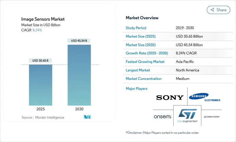
預計到 2025 年,影像感測器市場規模將達到 306.5 億美元,到 2030 年將擴大到 455.4 億美元,預測期內複合年成長率將達到 8.24%。
這一成長反映了汽車安全法規、先進的多攝影機智慧型手機以及工業自動化需求的共同作用,這些因素正在再形成半導體需求。汽車製造商計畫在2025年每輛車平均增加8個攝影機,到2028年增加12個攝影機,這將加速感測器產量和平均售價的擴張。由於低功耗的片上處理能力,CMOS元件將在2024年佔據93%的出貨量,而堆疊式背照式(BSI)設計到2030年將以55%的複合年成長率成長,從而在邊緣端實現更高的動態範圍和人工智慧運算能力。 4-12MP解析度區間佔據主導地位,佔總收入的32%,在主流消費和工業應用領域兼顧了影像品質和成本。在地緣政治出口限制、300mm晶圓短缺以及熱噪聲阻礙亞微米像素尺寸縮小等因素的影響下,SONY、三星、OmniVision和安森美半導體正在激烈競爭,以抵禦新參與企業的市場佔有率。
全球影像感測器市場趨勢與洞察
汽車影像感測器促進了ADAS和自動駕駛技術的普及。
安森美半導體 (Onsemi) 的 Hyperlux AR0823AT 晶片成功入選Subaru下一代 EyeSight 立體攝影機系統,並達到了自主決策所需的 ASIL-C 安全等級。Canon的 410MP 原型感測器實現了 3280MP/s 的處理速度,證明現代感測器已不再是成像器,而是計算平台。SONY預測,2019 年至 2030 年間,汽車攝影機節點數量將增加 6.68 倍,凸顯了 OEM 廠商對高動態範圍、低延遲組件的持續需求。 HDR、LED 閃爍抑制和功能安全 IP 現已成為標配,使汽車成像器成為關鍵的安全基礎設施。
亞洲地區配備高解析度CMOS BSI感測器的多相機智慧型手機的滲透率
亞洲行動電話系統持續推動像素架構的突破。三星計劃從2025年開始將其華城生產線改造為堆疊式CIS製造,力爭贏得高階iPhone的設計訂單。這種三層感測器將光電二極體層、傳輸和邏輯層分離,在縮小尺寸的同時提升了動態範圍。 OmniVision的OV50X採用1.6µm像素實現了110dB的單次曝光HDR,證明了亞洲供應商在低照度計算成像領域的領先地位。從百萬像素競爭轉向影像品質競爭,凸顯了智慧型手機發展週期的日趨成熟,先進的BSI和AI ISP的整合將顯著提升用戶體驗。
300毫米晶圓製造供應鏈的集中導致價格波動。
儘管SEMI預測2024年晶圓月產能將達到3000萬片,但生產集中在少數幾家亞洲晶圓代工廠,加劇了需求激增期間的供不應求。目前,影像感測器生產線正與利潤更高的AI加速器生產線爭奪相同的300毫米光刻設備,導致晶粒價格上漲和前置作業時間延長。據麥肯錫稱,微影術所需的特種化學品有60%並非在美國本土供應,增加了上游風險。在亞利桑那州和歐洲的晶圓廠從2026年開始逐步實現量產之前,價格波動可能會持續對整個影像感測器市場的利潤率構成壓力。
細分市場分析
到2024年,CMOS感測器將佔出貨量的93%,從而支援低功耗邏輯整合和晶圓成本優勢。 CMOS影像感測器市場規模將在2025年達到287億美元,超過CCD市場。列並行ADC和背面互連技術提高了影格速率,同時縮小了晶粒面積,使得供應商僅在行動電話的年出貨量就達到50億至70億片。儘管科學研究和醫療設備仍因其超低暗電流而繼續訂購CCD,但晶圓廠的投資正逐漸轉向CMOS,CCD的市佔率穩定成長。三星的三層堆疊結構透過分離光電二極體、傳輸層和邏輯層,提高了量子效率並降低了串擾,鞏固了CMOS的領先地位。
第二代堆疊式CIS工藝,憑藉其改進的冗餘性和缺陷管理能力,預計到2030年CMOS製程的複合年成長率將達到10.2%。這一成長動能將使來自中國和印度的新興參與企業能夠獲得成熟的65nm製程授權,並推出具有競爭力的汽車環景顯示圖像感測器。隨著代工廠為光電模組增加專用的氧化物-絕緣體埋線和混合鍵合線,CMOS創新仍然是影像感測器市場的主要驅動力。
堆疊式背照式感測器 (BSI) 的出貨量正以 55% 的複合年成長率成長,垂直整合突破了2D縮放的限制。光電二極體層和邏輯層的分離使得在不增加晶粒下,能夠獲得更大的集光面積,從而實現 1.5-2EV 的感光度提升。Canon的 410MP 堆疊式全片幅感測器透過 40 條平行通道實現了 3280MP/s 的讀取速度,展現了其高性能潛力。晶圓間混合鍵結技術正從試生產階段逐步邁向全天候量產,顯著提升了製造產量比率,與矽通孔堆疊技術相比,成本降低了 30%。
在影像感測器市場,受智慧型手機和車載高級駕駛輔助系統(ADAS)日益成長的推動,堆疊式背照式(BSI)預計到2030年將佔據259億美元的市場佔有率。雖然正面BSI和傳統BSI仍將是成本主導型低階設備的可行選擇,但高階製造商目前正圍繞多層堆疊技術調整藍圖,這些技術將ISP模組、SDRAM和AI加速器整合到像素矩陣下方,從而推動系統級封裝)的整合。
區域分析
北美仍然是該地區最大的區域買家,ADAS法規和國防採購推動了高規格ASP的需求。美國最終確定了自動緊急煞車規則,該規則實際上強制要求從2029年起所有輕型車輛安裝前置攝影機,從而鎖定了長期需求。加拿大的一級供應商正湧向安大略省的汽車產業走廊,墨西哥則為美國OEM廠商提供模組組裝。該地區半導體自主研發的措施正促使台積電位於亞利桑那州的巨型晶圓廠(投資額達1,650億美元)從2027年起供應成熟節點的CIS晶圓。
歐洲強調以隱私為先的智慧城市,透過《晶片法案》為邊緣人工智慧影像感測器提供資金,歐司朗在奧地利投資 5.88 億歐元進行擴張,將同時供應汽車雷射雷達和市政交通節點,德國和法國實施了 Euro-NCAP 攝影機基準測試,這將對整個歐洲大陸的供應商產生連鎖反應,地方法規限制了臉部雲端數據的儲存,並鼓勵了面部內雲和設備內推理感測器。
亞太地區擁有全球最大的晶圓產能和最高的出貨量成長率。日本SONY憑藉與一級製造商的合作,目標是在2026年佔據汽車CMOS市場43%的佔有率。韓國三星正在對其華城工廠進行改造,以每月增加20萬片晶圓的CIS產能,從而支援智慧型手機和AR/VR相機。中國吉林一號衛星星座的遙感探測需求不斷成長,但由於美國對先進的28nm CIS製程節點實施出口限制,國內晶圓代工廠正加速投資成熟製程。印度正在崛起為以消費主導的汽車行車記錄器和低成本行動電話市場,而以色列正在其GaAs晶圓廠開發小眾國防成像器,進一步擴大了區域多元化。
其他福利:
- Excel格式的市場預測(ME)表
- 3個月的分析師支持
目錄
第1章 引言
- 研究假設和市場定義
- 調查範圍
第2章調查方法
第3章執行摘要
第4章 市場情勢
- 市場概覽
- 市場促進因素
- 汽車級影像感測器加速了ADAS和自動駕駛系統的部署
- 亞洲地區配備高解析度CMOS BSI感測器的多相機智慧型手機的滲透率
- 短波紅外線/近紅外線感測器在精密農業和工業檢測的應用日益廣泛
- 邊緣人工智慧視覺模組加速了物聯網和智慧城市計劃的發展,尤其是在歐洲。
- 全球對AR/VR穿戴式裝置百葉窗感測器的需求正在上升。
- 北美和日本政府對ADAS攝影機的安全要求
- 市場限制
- 300毫米晶圓廠供應鏈集中導致價格波動
- 亞微米像素矽的熱雜訊和功耗限制,以及進一步提高解析度所面臨的挑戰
- 對先進成像晶片的出口限制影響中國原始設備製造商
- 短波紅外線感測器的高整合成本限制了其在消費性電子產品中的應用。
- 價值/供應鏈分析
- 監理展望
- 技術展望
- 波特五力分析
- 供應商的議價能力
- 消費者議價能力
- 新進入者的威脅
- 替代品的威脅
- 競爭對手之間的競爭
- 新冠疫情與以色列-加薩衝突的影響評估
第5章 市場規模與成長預測
- 按類型
- CMOS
- CCD
- 透過加工技術
- 前側照明(FSI)
- 背照式(BSI)
- 堆疊式BSI
- 按百葉窗類型
- 百葉窗
- 全球百葉窗
- 頻譜
- 可見光(RGB)
- 近紅外線(NIR)
- 短波紅外線 (SWIR)
- X光/紫外線
- 通過決議
- 小於100萬像素
- 1-3 MP
- 4-12 MP
- 13-24 MP
- 2500萬像素或以上
- 按最終用戶行業分類
- 消費性電子產品
- 汽車與運輸
- 工業自動化與機器人
- 安全與監控
- 醫療保健和生命科學
- 航太/國防
- 其他(智慧城市、農業、海洋)
- 按地區
- 北美洲
- 美國
- 加拿大
- 墨西哥
- 歐洲
- 英國
- 德國
- 法國
- 義大利
- 其他歐洲地區
- 亞太地區
- 中國
- 日本
- 印度
- 韓國
- 亞太其他地區
- 中東
- 以色列
- 沙烏地阿拉伯
- 阿拉伯聯合大公國
- 土耳其
- 其他中東地區
- 非洲
- 南非
- 埃及
- 其他非洲地區
- 南美洲
- 巴西
- 阿根廷
- 其他南美洲
- 北美洲
第6章 競爭情勢
- 市場集中度
- 策略趨勢
- 市佔率分析
- 公司簡介
- Sony Group Corp.
- Samsung Electronics Co., Ltd.
- OmniVision Technologies, Inc.
- STMicroelectronics NV
- ON Semiconductor Corporation
- Canon Inc.
- Panasonic Holdings Corporation
- Teledyne DALSA Inc.
- ams OSRAM AG
- SK hynix Inc.
- GalaxyCore Inc.
- Hamamatsu Photonics KK
- SmartSens Technology
- PixArt Imaging Inc.
- Himax Technologies, Inc.
- Tower Semiconductor Ltd.
- Teledyne e2v
- Gpixel Inc.
- Forza Silicon Corp.
- Toshiba Electronic Devices and Storage Corp.
- Pyxalis SA
第7章 市場機會與未來展望
The image sensor market reached USD 30.65 billion in 2025 and is projected to expand to USD 45.54 billion by 2030, translating to an 8.24% CAGR over the forecast period.
Growth reflects a confluence of automotive safety mandates, sophisticated multi-camera smartphones, and industrial automation needs that are reshaping semiconductor demand. Vehicle makers are equipping an average of 8 cameras per car in 2025 and plan to add 12 cameras by 2028, accelerating sensor volumes and ASP expansion. CMOS devices capture 93% of 2024 unit shipments because of low-power on-chip processing, while stacked back-side-illuminated (BSI) designs, scaling at a 55% CAGR to 2030, unlock higher dynamic range and AI computation at the edge. The 4-12 MP resolution bracket dominates with 32% revenue because it balances image quality and cost for mainstream consumer and industrial use. Competitive intensity is rising as Sony, Samsung, OmniVision and onsemi defend share against new entrants amid geopolitical export controls, 300 mm wafer scarcity, and thermal-noise barriers that slow sub-micron pixel shrink.
Global Image Sensors Market Trends and Insights
Automotive-grade Image Sensors Fueling ADAS & Autonomous Deployment
Automotive safety regulation is shifting cameras from premium options to mandated equipment, transforming the image sensor market. onsemi's Hyperlux AR0823AT won Subaru's next-gen EyeSight stereo-camera slot, meeting ASIL-C targets for autonomous decision making. Canon's prototype 410 MP sensor processes 3,280 MP/s, showing that modern sensors are computational platforms, not passive imagers. Sony projects a 6.68-fold jump in car camera nodes between 2019 and 2030, highlighting sustained OEM pull for high-dynamic-range, low-latency parts. HDR, LED-flicker mitigation and functional-safety IP now come standard, positioning automotive imagers as critical safety infrastructure.
Penetration of Multi-Camera Smartphones with High-Resolution CMOS BSI Sensors in Asia
Asia's handset ecosystem keeps driving pixel-architecture breakthroughs. Samsung converted its Hwaseong line to stacked CIS fabrication starting 2025, chasing premium iPhone design wins. Its 3-layer sensor splits photodiode, transfer and logic strata, boosting dynamic range while shrinking footprint. OmniVision's OV50X delivers 110 dB single-exposure HDR with 1.6 µm pixels, proving Asian suppliers now lead in low-light computational imaging. The shift from megapixel race to image quality underscores a mature smartphone cycle where advanced BSI and AI ISP integration differentiate user experience.
Supply-Chain Concentration in 300 mm Wafer Fabs Creating Price Volatility
SEMI records 30 million wafers-per-month capacity in 2024, yet production clusters around a handful of Asian foundries, amplifying shortages during demand spikes. Image sensor lines now compete with high-margin AI accelerators for the same 300 mm tools, lifting die prices and lengthening lead times. McKinsey observes that 60% of specialty chemicals needed for lithography lack local US supply, adding upstream risk. Until Arizona and European fabs reach volume after 2026, price swings will compress margins across the image sensor market.
Other drivers and restraints analyzed in the detailed report include:
- Growing Adoption of SWIR/NIR Sensors in Precision Agriculture & Industrial Inspection
- Edge-AI-Enabled Vision Modules Accelerating IoT & Smart City Projects
- Thermal Noise & Power Limits in Sub-Micron Pixel Shrink Challenging Further Resolution Gains
For complete list of drivers and restraints, kindly check the Table Of Contents.
Segment Analysis
CMOS sensors owned 93% of unit shipments in 2024, underscoring their low-power logic integration and per-wafer economics. The image sensor market size for CMOS reached USD 28.7 billion in 2025, dwarfing CCD revenues. Column-parallel ADC and backside wiring lift frame rate while shrinking die area, letting vendors ship 5-7 billion parts yearly for phones alone. Scientific and medical instruments continue ordering CCDs for ultra-low dark current, yet fab investments trend to CMOS, ensuring its share rises. Samsung's 3-layer stack demonstrates how separating photodiode, transfer and logic planes lifts quantum efficiency and reduces crosstalk, cementing CMOS leadership.
Second-generation stacked CIS improves redundancy and defect management, driving a projected 10.2% unit CAGR for CMOS through 2030. This momentum allows new entrants from China and India to license mature-node 65 nm flows and still launch competitive imagers for automotive surround-view. The image sensor market remains anchored on CMOS innovation as foundries add buried oxide isolation and hybrid bonding lines dedicated to photonics modules.
Stacked BSI shipments are growing at 55% CAGR because vertical integration circumvents 2-D scaling limits. Separating photodiode and logic layers permits larger light-collection areas without enlarging die, yielding 1.5-2 EV sensitivity uplift. Canon's 410 MP stacked full-frame sensor reads 3,280 MP/s via 40 parallel lanes, showing high-performance potential. Manufacturing yields have risen as wafer-to-wafer hybrid bonding moves from pilot to 24/7 production, cutting cost by 30% versus through-silicon-via stacking.
Within the image sensor market, stacked BSI is forecast to command USD 25.9 billion of image sensor market size by 2030, underpinned by smartphone and automotive ADAS volume ramps. Front-side and conventional BSI remain viable in low-tier devices where cost dominates, but premium makers now align roadmaps around multi-layer stacks that embed ISP blocks, SDRAM and AI accelerators under the pixel matrix, driving system-in-package convergence.
The Image Sensor Market Report is Segmented by Type (CMOS, CCD), Processing Technology (Front-Side Illuminated, Back-Side Illuminated, and More), Shutter Type (Rolling, Global), Spectrum (Visible, Near-Infrared, and More), Resolution (Less Than1 MP, 1-3 MP, and More), End-User Industry (Consumer Electronics, Automotive, Industrial, and More), and Geography. The Market Forecasts are Provided in Terms of Value (USD).
Geography Analysis
North America remains the largest regional buyer measured in revenue because ADAS regulations and defense procurements drive high-spec ASP. The United States finalized automatic emergency braking rules that implicitly require forward-facing cameras in all light vehicles from 2029, locking long-tail demand. Canada's Tier-1 suppliers cluster around Ontario's automotive corridor, and Mexico hosts module assembly for US OEMs. The region's push for semiconductor sovereignty spurred TSMC's USD 165 billion Arizona megafab, anticipated to supply mature-node CIS wafers post-2027.
Europe emphasizes privacy-first smart cities, funding edge-AI image sensors via the Chips Act. ams OSRAM's EUR 588 million Austrian expansion will feed both automotive lidar and municipal traffic nodes. Germany and France enforce Euro-NCAP camera benchmarks that trickle to suppliers across the continent. Local regulations cap cloud storage of facial data, encouraging in-sensor encryption and on-device inference, cultivating a premium for secure image sensor market designs.
Asia-Pacific houses most wafer capacity and posts the fastest shipment growth. Japan's Sony aims for 43% automotive CMOS share by 2026 on the back of Tier-1 alliances. South Korea's Samsung is retooling Hwaseong for additional 200,000 wafers-per-month CIS output to backfill smartphone and AR/VR cameras. China increases remote-sensing demand for its Jilin-1 constellation yet faces US export controls on advanced 28 nm CIS nodes, prompting domestic foundries to accelerate mature-process investments. India emerges as a consumption-driven market for automotive dash-cams and low-cost phones, while Israel develops niche defense imagers in GaAs fabs, extending regional diversity.
- Sony Group Corp.
- Samsung Electronics Co., Ltd.
- OmniVision Technologies, Inc.
- STMicroelectronics N.V.
- ON Semiconductor Corporation
- Canon Inc.
- Panasonic Holdings Corporation
- Teledyne DALSA Inc.
- ams OSRAM AG
- SK hynix Inc.
- GalaxyCore Inc.
- Hamamatsu Photonics K.K.
- SmartSens Technology
- PixArt Imaging Inc.
- Himax Technologies, Inc.
- Tower Semiconductor Ltd.
- Teledyne e2v
- Gpixel Inc.
- Forza Silicon Corp.
- Toshiba Electronic Devices and Storage Corp.
- Pyxalis S.A.
Additional Benefits:
- The market estimate (ME) sheet in Excel format
- 3 months of analyst support
TABLE OF CONTENTS
1 INTRODUCTION
- 1.1 Study Assumptions and Market Definition
- 1.2 Scope of the Study
2 RESEARCH METHODOLOGY
3 EXECUTIVE SUMMARY
4 MARKET LANDSCAPE
- 4.1 Market Overview
- 4.2 Market Drivers
- 4.2.1 Automotive-grade Image Sensors Fueling ADAS and Autonomous Deployment
- 4.2.2 Penetration of Multi-Camera Smartphones with High-Resolution CMOS BSI Sensors in Asia
- 4.2.3 Growing Adoption of SWIR/NIR Sensors in Precision Agriculture and Industrial Inspection
- 4.2.4 Edge-AI-Enabled Vision Modules Accelerating IoT and Smart City Projects, Especially in Europe
- 4.2.5 Rising Demand for Global Shutter Sensors in AR/VR Wearables
- 4.2.6 Government Safety Mandates for ADAS Cameras in North America and Japan
- 4.3 Market Restraints
- 4.3.1 Supply-Chain Concentration in 300 mm Wafer Fabs Creating Price Volatility
- 4.3.2 Thermal Noise and Power Limits in Sub-Micron Pixel Shrink Challenging Further Resolution Gains
- 4.3.3 Export Controls on Advanced Imaging Chips Affecting China-Based OEMs
- 4.3.4 High Integration Cost of SWIR Sensors Limiting Consumer Electronics Adoption
- 4.4 Value / Supply-Chain Analysis
- 4.5 Regulatory Outlook
- 4.6 Technological Outlook
- 4.7 Porter's Five Forces Analysis
- 4.7.1 Bargaining Power of Suppliers
- 4.7.2 Bargaining Power of Consumers
- 4.7.3 Threat of New Entrants
- 4.7.4 Threat of Substitutes
- 4.7.5 Intensity of Competitive Rivalry
- 4.8 Assessment on the Impact of COVID-19 and Israel-Gaza Conflict
5 MARKET SIZE AND GROWTH FORECASTS (VALUE)
- 5.1 By Type
- 5.1.1 CMOS
- 5.1.2 CCD
- 5.2 By Processing Technology
- 5.2.1 Front-Side Illuminated (FSI)
- 5.2.2 Back-Side Illuminated (BSI)
- 5.2.3 Stacked BSI
- 5.3 By Shutter Type
- 5.3.1 Rolling Shutter
- 5.3.2 Global Shutter
- 5.4 By Spectrum
- 5.4.1 Visible (RGB)
- 5.4.2 Near-Infrared (NIR)
- 5.4.3 Short-Wave Infrared (SWIR)
- 5.4.4 X-ray / UV
- 5.5 By Resolution
- 5.5.1 Less than 1 MP
- 5.5.2 1-3 MP
- 5.5.3 4-12 MP
- 5.5.4 13-24 MP
- 5.5.5 Greater than or Equal to 25 MP
- 5.6 By End-User Industry
- 5.6.1 Consumer Electronics
- 5.6.2 Automotive and Transportation
- 5.6.3 Industrial Automation and Robotics
- 5.6.4 Security and Surveillance
- 5.6.5 Healthcare and Life Sciences
- 5.6.6 Aerospace and Defense
- 5.6.7 Others (Smart City, Agriculture, Marine)
- 5.7 By Geography
- 5.7.1 North America
- 5.7.1.1 United States
- 5.7.1.2 Canada
- 5.7.1.3 Mexico
- 5.7.2 Europe
- 5.7.2.1 United Kingdom
- 5.7.2.2 Germany
- 5.7.2.3 France
- 5.7.2.4 Italy
- 5.7.2.5 Rest of Europe
- 5.7.3 Asia-Pacific
- 5.7.3.1 China
- 5.7.3.2 Japan
- 5.7.3.3 India
- 5.7.3.4 South Korea
- 5.7.3.5 Rest of Asia-Pacific
- 5.7.4 Middle East
- 5.7.4.1 Israel
- 5.7.4.2 Saudi Arabia
- 5.7.4.3 United Arab Emirates
- 5.7.4.4 Turkey
- 5.7.4.5 Rest of Middle East
- 5.7.5 Africa
- 5.7.5.1 South Africa
- 5.7.5.2 Egypt
- 5.7.5.3 Rest of Africa
- 5.7.6 South America
- 5.7.6.1 Brazil
- 5.7.6.2 Argentina
- 5.7.6.3 Rest of South America
- 5.7.1 North America
6 COMPETITIVE LANDSCAPE
- 6.1 Market Concentration
- 6.2 Strategic Moves
- 6.3 Market Share Analysis
- 6.4 Company Profiles (includes Global level Overview, Market level overview, Core Segments, Financials as available, Strategic Information, Market Rank/Share, Products and Services, Recent Developments)
- 6.4.1 Sony Group Corp.
- 6.4.2 Samsung Electronics Co., Ltd.
- 6.4.3 OmniVision Technologies, Inc.
- 6.4.4 STMicroelectronics N.V.
- 6.4.5 ON Semiconductor Corporation
- 6.4.6 Canon Inc.
- 6.4.7 Panasonic Holdings Corporation
- 6.4.8 Teledyne DALSA Inc.
- 6.4.9 ams OSRAM AG
- 6.4.10 SK hynix Inc.
- 6.4.11 GalaxyCore Inc.
- 6.4.12 Hamamatsu Photonics K.K.
- 6.4.13 SmartSens Technology
- 6.4.14 PixArt Imaging Inc.
- 6.4.15 Himax Technologies, Inc.
- 6.4.16 Tower Semiconductor Ltd.
- 6.4.17 Teledyne e2v
- 6.4.18 Gpixel Inc.
- 6.4.19 Forza Silicon Corp.
- 6.4.20 Toshiba Electronic Devices and Storage Corp.
- 6.4.21 Pyxalis S.A.
7 MARKET OPPORTUNITIES AND FUTURE OUTLOOK
- 7.1 White-space and Unmet-Need Assessment
 影像感測器市場:2026-2032年全球市場預測(按感測器類型、波長範圍、解析度、處理方法、終端用戶產業和分銷管道分類)
 影像感測器市場報告:按技術、處理方法、頻譜、陣列類型、終端應用產業和地區分類(2026-2034 年)
 2026年全球車載監視攝影機市場報告2026年全球HDR影像訊號處理設備市場報告
 光學影像防手震(OIS)市場規模、佔有率和成長分析:按技術架構、執行器類型、應用、軸向方向和地區分類-2026-2033年產業預測
 影像感測器全球市場規模、佔有率、趨勢和成長分析報告(2026-2034)捲簾百葉窗影像感測器市場:按解析度、像素尺寸、技術和應用分類-2026-2032年全球預測
 影像感測器市場分析及預測(至2035年):按類型、產品類型、技術、應用、組件、設備、最終用戶、功能及安裝類型分類快門傳感器市場分析及預測(至2035年):按類型、產品、技術、組件、應用、材料類型、設備、最終用戶和功能分類新興影像感測器技術市場分析及預測(至2035年):按類型、產品類型、技術、組件、應用、材料類型、裝置、製程、最終用戶和功能分類