


 |
市場調查報告書
商品編碼
1851519
歐洲影像感測器:市場佔有率分析、行業趨勢、統計數據和成長預測(2025-2030 年)Europe Image Sensors - Market Share Analysis, Industry Trends & Statistics, Growth Forecasts (2025 - 2030) |
||||||
※ 本網頁內容可能與最新版本有所差異。詳細情況請與我們聯繫。
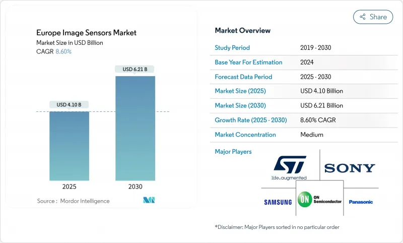
歐洲影像感測器市場預計到 2025 年將達到 41 億美元,到 2030 年將達到 62.1 億美元,年複合成長率為 8.66%。
對汽車安全需求的不斷成長、智慧型手機攝影機技術的創新以及歐盟半導體共享政策的推行,正共同推動價值創造從家用電子電器領域轉向高可靠性的汽車和工業細分市場。晶圓級光學堆疊CMOS成像感測器(CIS)架構與量子點材料在保持輕薄外形的同時,不斷提升性能上限。區域性廠商可以利用其與汽車製造商和工業OEM廠商的地理優勢,比遠距離供應商更快檢驗功能安全要求。同時,歐洲微影術設備出口限制的不確定性以及不斷上漲的能源價格,限制了近期產能擴張,使得廠商優先考慮技術領先優勢高於成本的高階細分市場。
歐洲影像感測器市場趨勢與洞察
智慧型手機多鏡頭競賽 > 200MP
為了與亞洲競爭對手抗衡,歐洲品牌正將感測器解析度提升至2億像素甚至更高。像素合併技術可在不增加檔案大小的情況下改善低照度性能,而晶圓級光學元件則可降低相機解析度的下降幅度。 OmniVision 的0.56微米像素證明了此技術的可行性,並凸顯了溫度控管的權衡取捨。如今,設備製造商非常重視歐洲封裝專家,他們能夠將光學元件、DSP和AI流水線整合到緊湊的外形規格中。隨著演算法的成熟和成本曲線的趨於平緩,這項技術的應用將從2026年開始逐步擴展。
歐洲新車安全評估協會(Euro NCAP)強制要求配備前置相機。
歐洲新車安全評鑑協會 (Euro NCAP) 的星級評定系統即將更新,屆時所有 2026 年後推出的新車都必須配備前置鏡頭,用於自動緊急煞車。此規則同樣適用於行人及騎乘者偵測,提高了感測器解析度和動態範圍的要求。安森美半導體 (OnSemi) 的 Hyperlux 系列產品提供 150dB HDR 解析度,專為高眩光路況最佳化,可縮短德國和義大利汽車製造商的檢驗時間。歐洲一級供應商受益於地理位置優勢,靠近測試場地和監管機構,從而縮短了從原型到量產的研發週期。
歐盟高昂的能源和無塵室設施成本
歐洲的電力和超純水成本比亞洲平均高出30%至50%。碳中和承諾迫使工廠預先支付再生能源合約和暖通空調升級費用。意法半導體(STMicroelectronics)提出的2027年實現碳中和的藍圖凸顯了資金方面的限制。規模較小的代工廠由於產量不足以抵消這些成本,要么退出市場,要么轉型為精簡型晶圓廠模式。歐洲影像感測器市場的參與者正面臨短期利潤壓力,但他們正在贏得注重環境、社會和治理(ESG)的買家的青睞,並建立良好的聲譽。
細分市場分析
CMOS感測器憑藉其低功耗和邏輯整合優勢,預計將在2024年佔據歐洲影像感測器市場86.30%的佔有率。而對移動車輛和機器人至關重要的全局百葉窗感測器,預計將以9.30%的複合年成長率成長,並在2030年佔據歐洲影像感測器市場的大部分佔有率。捲簾百葉窗CMOS感測器非常適合對價格敏感的行動電話和筆記型電腦,而CCD感測器則主要應用於對超低雜訊要求極高的科學領域。
歐洲企業正利用與汽車製造商的緊密合作關係,共同設計符合ASIL-B認證標準的全局百葉窗零件,從而提前鎖定Euro NCAP 2026款車型的設計訂單。晶圓級光學元件和深溝槽隔離技術在不增加晶粒尺寸的情況下提高了量子效率。因此,歐洲全局百葉窗裝置的影像感測器市場規模預計將強勁成長,即使在消費週期疲軟的情況下,也能增強該地區的收入韌性。
2024年,2,500萬至6,400萬像素的影像感測器將以28.44%的市佔率領先市場,在檔案大小和運算工作負載之間取得平衡。然而,2億像素以上的影像感測器市場將以12.33%的複合年成長率成長,這主要得益於旗艦行動電話無損數位變焦和8K視訊裁剪等功能的推動。隨著像素合併演算法的日益成熟,歐洲超高解析度影像感測器市場規模將在2025年至2030年間實現最快成長。
將晶圓級光學元件與亞微米像素對齊的先進封裝技術可減少鏡頭像差,使歐洲模組製造商能夠進入高階手機市場。據觀察,歐洲影像感測器市場的原始設備製造商(OEM)正在國內採購特種玻璃和IR濾鏡,以應對亞洲供應衝擊。入門級手機仍然依賴低於800萬像素的晶片,這些晶片受制於捲簾百葉窗的大規模生產。
其他福利:
- Excel格式的市場預測(ME)表
- 包含 3 個月的分析師支持
目錄
第1章 引言
- 研究假設和市場定義
- 調查範圍
第2章調查方法
第3章執行摘要
第4章 市場情勢
- 市場概覽
- 市場促進因素
- 智慧型手機競相推出2億像素以上相機
- 歐洲新車安全評鑑協會(Euro NCAP)強制要求前置相機(AEB)
- 晶圓級光學和堆疊式CIS的過渡
- 人工智慧賦能的工業機器視覺補貼
- 拋棄式晶片式醫用內視鏡
- 歐盟智慧城市監控競標
- 市場限制
- 歐盟能源成本高企,無塵室公用設施成本高昂
- 300mm CIS級鋼材產能有限
- 價值/供應鏈分析
- 監管環境
- 技術展望
- 波特五力分析
- 供應商的議價能力
- 買方的議價能力
- 新進入者的威脅
- 替代品的威脅
- 競爭對手之間的競爭
第5章 市場規模與成長預測
- 按類型
- CMOS
- CCD
- 通過決議
- 8 MP
- 924 MP
- 2564 MP
- 65200 MP
- 2億像素以上
- 頻譜
- 可見光(RGB)
- 近紅外線(NIR)
- 短波紅外線 (SWIR)
- 紫外線 (UV)
- 熱感/長波紅外線
- 透過百葉窗技術
- 捲簾百葉窗CMOS
- 全域百葉窗CMOS
- 按最終用戶行業分類
- 消費性電子產品
- 衛生保健
- 工業的
- 安全與監控
- 汽車與運輸
- 航太/國防
- 其他終端用戶產業
- 按國家/地區
- 英國
- 德國
- 法國
- 義大利
- 其他歐洲地區
第6章 競爭情勢
- 市場集中度
- 策略趨勢
- 市佔率分析
- 公司簡介
- STMicroelectronics
- Sony Corporation
- Samsung Electronics Co., Ltd
- On Semiconductor
- OmniVision Technologies
- BAE Systems
- Toshiba Electronic Devices and Storage
- Nikon Corp.
- Panasonic Corp.
- SK Hynix
- Canon Inc.
- AMS-Osram AG
- Teledyne FLIR
- Hamamatsu Photonics
- PixArt Imaging Inc.
- Tower Semiconductor
- Gpixel NV
- Himax Technologies
- GalaxyCore Inc.
- Teledyne e2v
第7章 市場機會與未來展望
The Europe image sensors market stands at USD 4.1 billion in 2025 and is projected to reach USD 6.21 billion by 2030, reflecting an 8.66% CAGR.
Pent-up automotive safety demand, smart-phone camera innovation and EU semiconductor re-shoring policies combine to move value creation from consumer electronics toward high-reliability automotive and industrial niches. Wafer-level optics stacked CMOS imaging sensor (CIS) architectures and quantum-dot materials increase performance ceilings while keeping form factors slim. Regional players leverage proximity to automakers and industrial OEMs to validate functional-safety requirements faster than distant suppliers can. At the same time, export-control uncertainty around lithography tools and high European energy prices temper near-term capacity expansion, pushing firms to prioritize premium segments where technical leadership outweighs cost.
Europe Image Sensors Market Trends and Insights
Multi-camera smartphone race >200 MP
European brands escalate sensor resolution beyond 200 MP to counter Asian rivals. Pixel-binning improves low-light results without ballooning file sizes, while wafer-level optics keeps camera bumps in check. OmniVision's 0.56 µm pixels prove technical feasibility and highlight thermal-management trade-offs. Device makers now value European packaging specialists that co-design optics, DSP and AI pipelines in tight form factors. Adoption is set to widen from 2026 as algorithms mature and cost curves bend.
Euro NCAP AEB front-camera mandate
Euro NCAP's updated star-rating system makes forward-facing cameras compulsory for Automatic Emergency Braking across new models launched from 2026. The rule extends to cyclist and pedestrian detection, increasing sensor resolution and dynamic-range targets. OnSemi's Hyperlux family delivers 150 dB HDR tuned for glare-filled road scenes, lowering validation time for German and Italian OEMs. European tier-1 suppliers benefit from geographical proximity to test tracks and regulatory bodies, shortening loop times between prototype and series production.
High EU energy and clean-room utility costs
Electricity and ultra-pure water bills in Europe sit 30-50% above Asian averages. Carbon-neutrality pledges force fabs to pre-pay for renewable power contracts and HVAC upgrades. STMicroelectronics' roadmap to reach carbon neutrality by 2027 exemplifies the capital drag. Smaller foundries lacking volume to offset these overheads either exit or pivot to fab-lite models. Europe image sensors market players see near-term margin squeeze yet gain reputational leverage with ESG-focused buyers.
Other drivers and restraints analyzed in the detailed report include:
- Wafer-level optics and stacked CIS migration
- AI-enabled industrial machine-vision grants
- Limited 300 mm CIS-grade capacity
For complete list of drivers and restraints, kindly check the Table Of Contents.
Segment Analysis
CMOS sensors captured 86.30% of Europe image sensors market share in 2024 on the back of lower power draw and logic integration. Global-shutter variants, vital for motion-heavy automotive and robotics tasks, are pacing at 9.30% CAGR and will command a larger slice of the Europe image sensors market by 2030. Rolling-shutter CMOS stays relevant for price-sensitive phones and laptops, while CCD retreats into scientific niches where ultra-low noise still matters.
European firms exploit close ties with automakers to co-design ASIL-B qualified global-shutter parts, gaining early design-wins for Euro NCAP 2026 models. Wafer-level optics and deep-trench isolation raise quantum efficiency without inflating die size. Consequently, Europe image sensors market size for global-shutter devices is projected to climb steadily, lifting regional revenue resilience even if consumer cycles soften.
The 25-64 MP class led revenue with 28.44% share in 2024, balancing file-size economy and computational workload. However, >200 MP parts rise at 12.33% CAGR, fuelled by flagship phones that tout lossless digital zoom and 8K video crops. Europe image sensors market size for these ultra-resolution devices will expand fastest in 2025-2030 as pixel-binning algorithms mature.
Packaging advances that align wafer-level optics with sub-µm pixels curb lens aberration, letting European module makers enter premium handset SKUs. The Europe image sensors market observes OEMs procuring specialty glass and IR filters domestically to hedge against Asian supply shocks. Entry-level handsets still rely on <=8 MP chips, keeping a floor under high-volume rolling-shutter production.
The Europe Image Sensors Market is Segmented by Type (CMOS, CCD), Resolution (<= 8 MP, 9 - 24 MP and More), Spectrum (Visible (RGB), Near-Infrared (NIR) and More), Shutter Technology, End-User Industry (Consumer Electronics, Healthcare, and More), and Country. The Market Forecasts are Provided in Terms of Value (USD).
List of Companies Covered in this Report:
- STMicroelectronics
- Sony Corporation
- Samsung Electronics Co., Ltd
- On Semiconductor
- OmniVision Technologies
- BAE Systems
- Toshiba Electronic Devices and Storage
- Nikon Corp.
- Panasonic Corp.
- SK Hynix
- Canon Inc.
- AMS-Osram AG
- Teledyne FLIR
- Hamamatsu Photonics
- PixArt Imaging Inc.
- Tower Semiconductor
- Gpixel NV
- Himax Technologies
- GalaxyCore Inc.
- Teledyne e2v
Additional Benefits:
- The market estimate (ME) sheet in Excel format
- 3 months of analyst support
TABLE OF CONTENTS
1 INTRODUCTION
- 1.1 Study Assumptions and Market Definition
- 1.2 Scope of the Study
2 RESEARCH METHODOLOGY
3 EXECUTIVE SUMMARY
4 MARKET LANDSCAPE
- 4.1 Market Overview
- 4.2 Market Drivers
- 4.2.1 Multi-camera smartphone race beyond 200 MP
- 4.2.2 Euro NCAP front-camera mandate (AEB)
- 4.2.3 Wafer-level optics and stacked CIS migration
- 4.2.4 AI-enabled industrial machine-vision grants
- 4.2.5 Disposable chip-on-tip medical endoscopy
- 4.2.6 EU smart-city surveillance tenders
- 4.3 Market Restraints
- 4.3.1 High EU energy and clean-room utility costs
- 4.3.2 Limited 300 mm CIS-grade capacity
- 4.4 Value / Supply-Chain Analysis
- 4.5 Regulatory Landscape
- 4.6 Technological Outlook
- 4.7 Porters Five Forces Analysis
- 4.7.1 Bargaining Power of Suppliers
- 4.7.2 Bargaining Power of Buyers
- 4.7.3 Threat of New Entrants
- 4.7.4 Threat of Substitutes
- 4.7.5 Intensity of Competitive Rivalry
5 MARKET SIZE AND GROWTH FORECASTS (VALUE)
- 5.1 By Type
- 5.1.1 CMOS
- 5.1.2 CCD
- 5.2 By Resolution
- 5.2.1 8 MP
- 5.2.2 924 MP
- 5.2.3 2564 MP
- 5.2.4 65200 MP
- 5.2.5 > 200 MP
- 5.3 By Spectrum
- 5.3.1 Visible (RGB)
- 5.3.2 Near-Infrared (NIR)
- 5.3.3 Short-Wave IR (SWIR)
- 5.3.4 Ultraviolet (UV)
- 5.3.5 Thermal / LWIR
- 5.4 By Shutter Technology
- 5.4.1 Rolling-Shutter CMOS
- 5.4.2 Global-Shutter CMOS
- 5.5 By End-User Industry
- 5.5.1 Consumer Electronics
- 5.5.2 Healthcare
- 5.5.3 Industrial
- 5.5.4 Security and Surveillance
- 5.5.5 Automotive and Transportation
- 5.5.6 Aerospace and Defense
- 5.5.7 Other End-user Industries
- 5.6 By Country
- 5.6.1 United Kingdom
- 5.6.2 Germany
- 5.6.3 France
- 5.6.4 Italy
- 5.6.5 Rest of Europe
6 COMPETITIVE LANDSCAPE
- 6.1 Market Concentration
- 6.2 Strategic Moves
- 6.3 Market Share Analysis
- 6.4 Company Profiles (includes Global-level Overview, Market-level Overview, Core Segments, Financials as available, Strategic Information, Market Rank/Share for key companies, Products and Services, and Recent Developments)
- 6.4.1 STMicroelectronics
- 6.4.2 Sony Corporation
- 6.4.3 Samsung Electronics Co., Ltd
- 6.4.4 On Semiconductor
- 6.4.5 OmniVision Technologies
- 6.4.6 BAE Systems
- 6.4.7 Toshiba Electronic Devices and Storage
- 6.4.8 Nikon Corp.
- 6.4.9 Panasonic Corp.
- 6.4.10 SK Hynix
- 6.4.11 Canon Inc.
- 6.4.12 AMS-Osram AG
- 6.4.13 Teledyne FLIR
- 6.4.14 Hamamatsu Photonics
- 6.4.15 PixArt Imaging Inc.
- 6.4.16 Tower Semiconductor
- 6.4.17 Gpixel NV
- 6.4.18 Himax Technologies
- 6.4.19 GalaxyCore Inc.
- 6.4.20 Teledyne e2v
7 MARKET OPPORTUNITIES AND FUTURE OUTLOOK
- 7.1 White-space and Unmet-need Assessment
 影像感測器市場:2026-2032年全球市場預測(按感測器類型、波長範圍、解析度、處理方法、終端用戶產業和分銷管道分類)
 2026年全球車載監視攝影機市場報告2026年全球HDR影像訊號處理設備市場報告
 光學影像防手震(OIS)市場規模、佔有率和成長分析:按技術架構、執行器類型、應用、軸向方向和地區分類-2026-2033年產業預測捲簾百葉窗影像感測器市場:按解析度、像素尺寸、技術和應用分類-2026-2032年全球預測
 影像感測器市場分析及預測(至2035年):按類型、產品類型、技術、應用、組件、設備、最終用戶、功能及安裝類型分類快門傳感器市場分析及預測(至2035年):按類型、產品、技術、組件、應用、材料類型、設備、最終用戶和功能分類新興影像感測器技術市場分析及預測(至2035年):按類型、產品類型、技術、組件、應用、材料類型、裝置、製程、最終用戶和功能分類
 全球影像感測器市場:按類型、成像技術、影像類型、解析度、應用、國家和地區分類-產業分析、市場規模、佔有率及未來預測(2025-2032年)2026年全球影像感測器市場報告