


 |
市場調查報告書
商品編碼
1849924
半導體封裝:市場佔有率分析、產業趨勢、統計數據和成長預測(2025-2030 年)Semiconductor Packaging - Market Share Analysis, Industry Trends & Statistics, Growth Forecasts (2025 - 2030) |
||||||
※ 本網頁內容可能與最新版本有所差異。詳細情況請與我們聯繫。
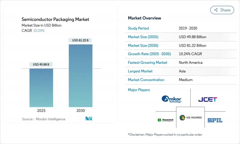
預計到 2025 年,半導體封裝市場規模將達到 498.8 億美元,到 2030 年將達到 812.2 億美元,2025 年至 2030 年的複合年成長率為 10.24%。
從成本驅動型組裝轉向性能驅動型整合正在推動這一成長。人工智慧工作負載對高頻寬記憶體和卓越散熱路徑的需求,正推動對2.5D和3D架構的快速需求。儘管產量仍依賴傳統的引線鍵合和導線架工藝,但價值創造正轉向扇出型晶圓層次電子構裝(WLP)和支援晶片組的中介層。汽車電氣化推動了高功率密度模組兩位數的成長,而智慧型手機和PC的更新換代週期則維持了消費領域的基準產量。從區域來看,亞洲佔全球產量的一半以上,但得益於《晶片法案》(CHIPS Act)的激勵措施為新建後端晶圓廠提供的資金,北美地區的複合年成長率(CAGR)最高。 ABF基板的供應瓶頸和先進工具的出口限制,是推動地理多元化和材料創新的催化劑。
全球半導體封裝市場趨勢與洞察
AI加速器熱潮推動2.5D/3D插層器的發展
台積電的CoWoS晶片產能將在2023年至2024年間加倍,從12萬片增加到24萬片,但仍無法完全滿足超大規模資料中心的需求。產能缺口促使業界探索替代性的面板級製程和3.5D堆疊測試,這些測試可將超過6000平方毫米的矽晶圓整合到單一封裝中。因此,先進封裝技術正從成本中心轉變為提升人工智慧系統效能的策略槓桿。
美國和亞洲的電動車動力組件
安森美半導體(ON Semiconductor)的EliteSiC平台已獲大眾汽車公司訂單,該平台代表了向具有卓越散熱性能的整合功率模組過渡的典範。羅姆(ROHM)的6合1模塑SiC模組的功率密度是傳統型號的三倍。這些創新產品集中在美國和亞洲的供應鏈,使其能夠滿足嚴格的汽車認證標準。
ABF基板供應供不應求
Nittobo在2025年8月漲價20%,暴露出系統性的材料短缺問題,尤其對覆晶BGA生產線造成了嚴重影響。台灣和日本產能有限,導致前置作業時間延長,迫使OEM廠商考慮採用玻璃和矽芯替代方案。
細分市場分析
到2024年,傳統的打線接合和導線架產品仍將佔據半導體封裝市場52.5%的佔有率(以出貨量計),確保家用電子電器和工業設備的材料成本保持在可負擔的範圍內。然而,扇出型WLP(晶圓級封裝)將以12.3%的複合年成長率超越所有其他封裝形式,這標誌著半導體封裝市場正向無基板的線路重布轉型,從而降低z軸高度並提高I/O密度。覆晶將透過結合小間距凸塊和適中的成本來填補這一市場空白,而SiP(系統級封裝)和PoP(封裝堆疊)架構則可實現垂直堆疊,從而滿足空間受限的行動裝置的需求。
在先進技術方面,2.5D中介層將高頻寬記憶體與AI邏輯晶片並排放置,而3D堆疊技術則能有效降低延遲。嵌入式晶粒和麵板級生產線正吸引著專注於物聯網價格分佈的新興參與企業,這標誌著半導體封裝市場正在分化為高性能節點和超低成本量產廠商兩大陣營。相較之下,面板級生產線的單腳價格低於0.10美元,凸顯了成本結構的差異。因此,設備製造商正在對其產品組合進行細分,用於3µm對準的高精度鍵合機叢集與用於物聯網標籤的大型面板模塑生產線並存。這種分化正在重新定義半導體封裝市場中供應商的定位。
到2024年,有機ABF基板將佔總收入的41.5%,為主流覆晶生態系統提供支援。然而,隨著汽車和產業部門延長成熟的鋁線和金線封裝的使用壽命,鍵合線半導體封裝市場規模預計將以每年11.4%的速度成長。導線架在重視銅散熱器性能的功率應用中仍然很受歡迎。封裝樹脂正在朝向高導熱等級發展,以支援下一代SiC和GaN模組。
2027年起,玻璃基板或將取代有機基板。英特爾和三星的原型產品展示了40%的通孔間距縮減和接近零的熱膨脹係數失配,從而減少了3D堆疊中的翹曲。在1200V牽引逆變器中,奈米鑽石填料被添加到導熱界面材料中,可將結間電阻降低30%。 2025年,金價上漲將壓縮顯示器驅動IC封裝的利潤空間,進而推動銅柱凸塊封裝的普及。
區域分析
到2024年,亞洲將佔據半導體封裝市場53.0%的佔有率,這主要得益於台灣在CoWoS領域的領先地位以及中國在引線鍵合組裝方面的規模優勢。江電科技在江蘇投資44億元建造的汽車級工廠將提升當地碳化矽功率封裝的產能。韓國受益於以記憶體為中心的SiP技術,而日本則在關鍵的基板化學領域佔據主導地位,從而鞏固了區域叢集的緊密聯繫。
預計到2030年,北美半導體封裝市場將以11.1%的複合年成長率成長。 《晶片封裝法案》(CHIPS Act)的獎勵措施已投資3億美元用於研發,並在亞利桑那州、新墨西哥州和加州打造了研發中心。例如,台積電與安靠在亞利桑那州的夥伴關係,在領先的晶圓廠附近建立了完整的後端生態系統。加拿大正在大力發展光電封裝,而墨西哥則為消費級ASIC晶片提供低成本的最終測試服務。
歐洲正鞏固其在汽車和工業的優勢。一家德國一級供應商正在共同開發一款雙面冷卻的碳化矽模組,目標是實現9kW/L的逆變器密度,這將推動對小眾OSAT(外包半導體組裝和測試)企業的投資。荷蘭正積極推動高頻光收發器的封裝技術,以配合垂直共振腔面射型雷射(VCSEL)的普及應用。中東和非洲仍在發展中,目前主要將組裝組裝給亞洲的製造中心,但正計劃根據主權指令,在國內建立用於安全物聯網和國防電子產品的生產線。
其他福利:
- Excel格式的市場預測(ME)表
- 3個月的分析師支持
目錄
第1章 引言
- 研究假設和市場定義
- 調查範圍
第2章調查方法
第3章執行摘要
第4章 市場情勢
- 市場概覽
- 市場促進因素
- AI加速器熱潮推動2.5D/3D插層器的發展
- 美國和亞洲的電動車動力組件
- 美國和歐盟的晶片獎勵催生了本地後端晶圓廠
- 中國和韓國對5G射頻SiP的需求
- 面向物聯網的超低成本面板級封裝
- 用於高密度中介層的晶片組架構
- 市場限制
- ABF基板供不應求(台灣/日本)
- 3D TSV/混合鍵結中的產量比率挑戰
- 中國對先進封裝工具的出口限制
- 扇出型 WLP <5 nm 散熱限制
- 價值/供應鏈分析
- 監理展望
- 技術展望
- 波特五力模型
- 供應商的議價能力
- 買方的議價能力
- 新進入者的威脅
- 替代品的威脅
- 競爭對手之間的競爭
- 產業能力與投資趨勢分析
- 定價分析
第5章 市場規模與成長預測
- 透過包裝平台
- 先進包裝
- 覆晶
- 扇出 WLP
- 扇入式 WLP
- 2.5D/3D IC
- 嵌入式晶粒
- SiP/PoP
- 面板級包裝
- 傳統包裝
- 引線鍵合
- 導線架
- QFN/QFP/SOP
- 先進包裝
- 透過包裝材料
- 有機基材物
- 導線架
- 連接線
- 封裝樹脂
- 陶瓷包裝
- 焊球和焊點凸起
- 晶片黏接和導熱矽脂
- 按晶圓尺寸
- 200毫米或更小
- 300 mm
- 450毫米或以上/面板
- 按經營模式
- OSAT
- 晶圓代工廠後端
- IDM內部
- 按最終用戶行業分類
- 消費性電子產品
- 智慧型手機和穿戴式裝置
- 計算/資料中心
- 汽車與出行
- ADAS/EV動力
- 通訊和電訊
- 5G基礎設施
- 航太與國防
- 醫療和保健設備
- 工業/能源(LED/電力)
- 消費性電子產品
- 按地區
- 北美洲
- 美國
- 加拿大
- 墨西哥
- 南美洲
- 巴西
- 其他南美洲
- 歐洲
- 德國
- 法國
- 英國
- 義大利
- 荷蘭
- 北歐國家
- 其他歐洲地區
- 中東和非洲
- 以色列
- 土耳其
- GCC
- 南非
- 其他中東和非洲地區
- 亞太地區
- 中國
- 台灣
- 韓國
- 日本
- 印度
- 新加坡
- 澳洲
- 紐西蘭
- 亞太其他地區
- 北美洲
第6章 競爭情勢
- 市場集中度
- 策略趨勢
- 市佔率分析
- 公司簡介
- ASE Technology Holding Co., Ltd.
- Amkor Technology, Inc.
- JCET Group Co., Ltd.
- Siliconware Precision Industries Co., Ltd.
- Powertech Technology Inc.
- Tianshui Huatian Technology Co., Ltd.
- UTAC Holdings Ltd.
- ChipMOS Technologies Inc.
- Chipbond Technology Corp.
- Intel Corporation
- Samsung Electronics Co., Ltd.
- Taiwan Semiconductor Manufacturing Co. Ltd.(TSMC)
- Micron Technology, Inc.
- Texas Instruments Inc.
- Advanced Micro Devices, Inc.
- Hana Micron Inc.
- Nepes Corporation
- TongFu Microelectronics Co., Ltd.
- Shinko Electric Industries Co., Ltd.
- Unisem(M)Berhad
第7章 市場機會與未來展望
The semiconductor packaging market size stood at USD 49.88 billion in 2025 and is projected to reach USD 81.22 billion by 2030, advancing at a 10.24% CAGR over 2025-2030.
A shift from cost-driven assembly toward performance-critical integration underpins this growth. Demand for 2.5D and 3D architectures has risen sharply as AI workloads call for high-bandwidth memory and superior thermal paths. Volume remains anchored in traditional wire-bond and lead-frame formats, yet value creation is migrating to fan-out wafer-level packaging (WLP) and chiplet-enabled interposers. Automotive electrification supports double-digit expansion in power-dense modules, while smartphone and PC refresh cycles sustain baseline volumes in the consumer segment. Regionally, Asia commands more than half of global output, but North America registers the highest CAGR thanks to CHIPS Act incentives that fund new back-end fabs. Supply bottlenecks in ABF substrates and export restrictions on advanced tools are catalyzing geographic diversification and material innovation.
Global Semiconductor Packaging Market Trends and Insights
AI accelerator boom driving 2.5D/3D interposers
TSMC's CoWoS capacity is doubling from 120,000 to 240,000 units between 2023 and 2024, yet it still cannot fully meet hyperscaler demand. The capacity gap is stimulating alternative panel-level flows and 3.5D stacking trials that aggregate more than 6,000 mm2 of silicon per package. Advanced packaging has therefore moved from a cost center to a strategic lever for AI system performance
Electrified-vehicle power packages in United States & Asia
onsemi's EliteSiC platform awarded by Volkswagen exemplifies the migration toward integrated power modules with superior heat dissipation. ROHM's 6-in-1 molded SiC modules deliver triple the power density of prior. These innovations concentrate in US and Asian supply chains that can meet stringent automotive qualification.
ABF substrate supply crunch
Nittobo's 20% price hike in August 2025 exposes systemic material tightness that particularly affects flip-chip BGA lines. Limited qualified capacity in Taiwan and Japan prolongs lead times and pushes OEMs to explore glass-core or silicon-core alternatives.
Other drivers and restraints analyzed in the detailed report include:
- US-EU CHIPS incentives creating local back-end fabs
- 5G RF-SiP demand in China & Korea
- Yield challenges in 3D TSV/hybrid bonding
For complete list of drivers and restraints, kindly check the Table Of Contents.
Segment Analysis
Traditional wire-bond and lead-frame offerings still dominated shipments with 52.5% semiconductor packaging market share in 2024, ensuring that consumer electronics and industrial devices retain affordable bill-of-materials costs. However, Fan-out WLP outpaces every other format at a 12.3% CAGR, signaling the semiconductor packaging market's move toward substrate-free redistribution layers that shrink z-height and boost I/O density. Flip-chip bridges the gap by pairing fine-pitch bumps with moderate cost, while SiP and PoP architectures enable vertical stacking for space-constrained handsets.
On the advanced front, 2.5D interposers position high-bandwidth memory adjacent to AI logic, and 3D stacks unlock latency gains. Embedded-die and panel-level flows attract new entrants focused on IoT price points, demonstrating that the semiconductor packaging market is splitting into premium performance nodes and ultra-low-cost volume plays. In contrast, panel-level lines deliver sub-USD 0.10 per pin, a ratio that underscores divergent cost structures. As a result, equipment makers have segmented their portfolios: high-accuracy bonder clusters for 3 µm alignment coexist with large-panel MOLD lines aimed at IoT tags. Such bifurcation redefines supplier positioning inside the semiconductor packaging market.
Organic ABF substrates carried 41.5% revenue in 2024, underpinning the mainstream flip-chip ecosystem. Yet semiconductor packaging market size for bonding wires is set to grow 11.4% annually as automotive and industrial sectors extend the life of proven aluminum and gold wire packages. Leadframes persist in power applications that value copper heat-spreader performance. Encapsulation resins have progressed to high-thermal-conductivity grades, supporting next-generation SiC and GaN modules.
Glass substrates could displace organic builds after 2027. Intel and Samsung prototypes show 40% via pitch reduction and near-zero CTE mismatch, lowering warpage in 3D stacks. Thermal interface materials now integrate nano-diamond fillers, cutting junction-to-case resistance by 30% in 1,200 V traction inverters. Gold price spikes compressed margins for display driver IC packaging in 2025, motivating migration to copper column bumps
The Semiconductor Packaging Market is Segmented by Packaging Platform (Advanced Packaging, Traditional Packaging), Packaging Material (Organic Substrates, and More), Wafer Size (<= 200 Mm, and More), Business Model (OSAT, and More) End-User Industry (Consumer Electronics, Aerospace and Defense and More), and by Geography. The Market Forecasts are Provided in Terms of Value (USD).
Geography Analysis
Asia captured 53.0% of the semiconductor packaging market in 2024, cemented by Taiwan's CoWoS monopoly and China's scale in wire-bond assembly. JCET's RMB 4.4 billion automotive plant in Jiangsu advances local competency in SiC power packages. South Korea benefits from memory-centric SiP, whereas Japan controls pivotal substrate chemistries, reinforcing a tightly knit regional cluster.
North America's semiconductor packaging market is projected to post an 11.1% CAGR through 2030. CHIPS Act incentives amass USD 300 million for R&D lines, spawning hubs in Arizona, New Mexico and California. Partnerships such as TSMC-Amkor in Arizona build complete back-end ecosystems proximate to leading-edge wafer fabs. Canada cultivates photonics packaging, and Mexico offers low-cost final test for consumer ASICs.
Europe positions around automotive and industrial strength. German Tier-1s co-develop double-sided cooled SiC modules targeting 9 kW/L inverter density, catalyzing niche OSAT investment. The Netherlands pushes high-frequency optical transceiver packaging that aligns with vertical-cavity surface-emitting laser (VCSEL) adoption. Middle East and Africa remain emerging, primarily outsourcing assembly to Asian hubs yet planning domestic lines for secure IoT and defense electronics under sovereign mandates.
- ASE Technology Holding Co., Ltd.
- Amkor Technology, Inc.
- JCET Group Co., Ltd.
- Siliconware Precision Industries Co., Ltd.
- Powertech Technology Inc.
- Tianshui Huatian Technology Co., Ltd.
- UTAC Holdings Ltd.
- ChipMOS Technologies Inc.
- Chipbond Technology Corp.
- Intel Corporation
- Samsung Electronics Co., Ltd.
- Taiwan Semiconductor Manufacturing Co. Ltd. (TSMC)
- Micron Technology, Inc.
- Texas Instruments Inc.
- Advanced Micro Devices, Inc.
- Hana Micron Inc.
- Nepes Corporation
- TongFu Microelectronics Co., Ltd.
- Shinko Electric Industries Co., Ltd.
- Unisem (M) Berhad
Additional Benefits:
- The market estimate (ME) sheet in Excel format
- 3 months of analyst support
TABLE OF CONTENTS
1 INTRODUCTION
- 1.1 Study Assumptions and Market Definition
- 1.2 Scope of the Study
2 RESEARCH METHODOLOGY
3 EXECUTIVE SUMMARY
4 MARKET LANDSCAPE
- 4.1 Market Overview
- 4.2 Market Drivers
- 4.2.1 AI Accelerator Boom Driving 2.5D/3D Interposers
- 4.2.2 Electrified Vehicle Power Packages in United States and Asia
- 4.2.3 US-EU CHIPS Incentives Creating Local Back-End Fabs
- 4.2.4 5G RF-SiP Demand in China and Korea
- 4.2.5 Panel Level Packaging for Ultra-Low-Cost IoT
- 4.2.6 Chiplet Architectures Powering High-Density Interposers
- 4.3 Market Restraints
- 4.3.1 ABF Substrate Supply Crunch (Taiwan/Japan)
- 4.3.2 Yield Challenges in 3D TSV/Hybrid Bonding
- 4.3.3 Export Controls on Advanced Packaging Tools to China
- 4.3.4 Thermal Dissipation Limits in Fan-Out WLP <5 nm
- 4.4 Value / Supply-Chain Analysis
- 4.5 Regulatory Outlook
- 4.6 Technological Outlook
- 4.7 Porter's Five Forces
- 4.7.1 Bargaining Power of Suppliers
- 4.7.2 Bargaining Power of Buyers
- 4.7.3 Threat of New Entrants
- 4.7.4 Threat of Substitutes
- 4.7.5 Intensity of Competitive Rivalry
- 4.8 Industry Capacity and Investment Trend Analysis
- 4.9 Pricing Analysis
5 MARKET SIZE AND GROWTH FORECASTS (VALUE)
- 5.1 By Packaging Platform
- 5.1.1 Advanced Packaging
- 5.1.1.1 Flip-Chip
- 5.1.1.2 Fan-Out WLP
- 5.1.1.3 Fan-In WLP
- 5.1.1.4 2.5D / 3D IC
- 5.1.1.5 Embedded-Die
- 5.1.1.6 SiP / PoP
- 5.1.1.7 Panel-Level Packaging
- 5.1.2 Traditional Packaging
- 5.1.2.1 Wire-Bond
- 5.1.2.2 Leadframe
- 5.1.2.3 QFN / QFP / SOP
- 5.1.1 Advanced Packaging
- 5.2 By Packaging Material
- 5.2.1 Organic Substrates
- 5.2.2 Leadframes
- 5.2.3 Bonding Wires
- 5.2.4 Encapsulation Resins
- 5.2.5 Ceramic Packages
- 5.2.6 Solder Balls and Bumps
- 5.2.7 Die-Attach and TIMs
- 5.3 By Wafer Size
- 5.3.1 <= 200 mm
- 5.3.2 300 mm
- 5.3.3 >= 450 mm / Panel
- 5.4 By Business Model
- 5.4.1 OSAT
- 5.4.2 Foundry Back-End
- 5.4.3 IDM In-house
- 5.5 By End-user Industry
- 5.5.1 Consumer Electronics
- 5.5.1.1 Smartphones and Wearables
- 5.5.1.2 Computing / Data-Center
- 5.5.1.3 Automotive and Mobility
- 5.5.1.3.1 ADAS / EV Power
- 5.5.1.4 Communications and Telecom
- 5.5.1.4.1 5G Infrastructure
- 5.5.1.5 Aerospace and Defense
- 5.5.1.6 Medical and Healthcare Devices
- 5.5.1.7 Industrial and Energy (LED / Power)
- 5.5.1 Consumer Electronics
- 5.6 By Geography
- 5.6.1 North America
- 5.6.1.1 United States
- 5.6.1.2 Canada
- 5.6.1.3 Mexico
- 5.6.2 South America
- 5.6.2.1 Brazil
- 5.6.2.2 Rest of South America
- 5.6.3 Europe
- 5.6.3.1 Germany
- 5.6.3.2 France
- 5.6.3.3 United Kingdom
- 5.6.3.4 Italy
- 5.6.3.5 Netherlands
- 5.6.3.6 Nordics
- 5.6.3.7 Rest of Europe
- 5.6.4 Middle East and Africa
- 5.6.4.1 Israel
- 5.6.4.2 Turkey
- 5.6.4.3 GCC
- 5.6.4.4 South Africa
- 5.6.4.5 Rest of Middle East and Africa
- 5.6.5 APAC
- 5.6.5.1 China
- 5.6.5.2 Taiwan
- 5.6.5.3 South Korea
- 5.6.5.4 Japan
- 5.6.5.5 India
- 5.6.5.6 Singapore
- 5.6.5.7 Australia
- 5.6.5.8 New Zealand
- 5.6.5.9 Rest of APAC
- 5.6.1 North America
6 Competitive Landscape
- 6.1 Market Concentration
- 6.2 Strategic Moves
- 6.3 Market Share Analysis
- 6.4 Company Profiles (includes Global level Overview, Market level overview, Core Segments, Financials as available, Strategic Information, Market Rank/Share, Products & Services, Recent Developments)
- 6.4.1 ASE Technology Holding Co., Ltd.
- 6.4.2 Amkor Technology, Inc.
- 6.4.3 JCET Group Co., Ltd.
- 6.4.4 Siliconware Precision Industries Co., Ltd.
- 6.4.5 Powertech Technology Inc.
- 6.4.6 Tianshui Huatian Technology Co., Ltd.
- 6.4.7 UTAC Holdings Ltd.
- 6.4.8 ChipMOS Technologies Inc.
- 6.4.9 Chipbond Technology Corp.
- 6.4.10 Intel Corporation
- 6.4.11 Samsung Electronics Co., Ltd.
- 6.4.12 Taiwan Semiconductor Manufacturing Co. Ltd. (TSMC)
- 6.4.13 Micron Technology, Inc.
- 6.4.14 Texas Instruments Inc.
- 6.4.15 Advanced Micro Devices, Inc.
- 6.4.16 Hana Micron Inc.
- 6.4.17 Nepes Corporation
- 6.4.18 TongFu Microelectronics Co., Ltd.
- 6.4.19 Shinko Electric Industries Co., Ltd.
- 6.4.20 Unisem (M) Berhad
7 MARKET OPPORTUNITIES AND FUTURE OUTLOOK
- 7.1 White-space and Unmet-Need Assessment
 3-D TSV:關鍵問題洞察與市場分析
 半導體原型製作和封裝市場分析及至2034年的預測:類型、產品、服務、技術、應用、材料類型、組件、流程、最終用戶、設備
 高密度封裝(MCM、MCP、SIP、3D-TSV):市場分析與技術趨勢
 全球 3D 半導體封裝市場:未來預測(至 2032 年)—材料、技術、最終用戶和地區分析
 2025年先進晶片封裝全球市場報告2025年全球3D半導體封裝市場報告
 半導體先進封裝市場(按平台、材料類型、組件、間距、應用和最終用途行業)- 全球預測,2025 年至 2030 年2025年全球四方扁平封裝市場報告先進晶片封裝市場(按封裝類型和地區)
 日本半導體封裝市場規模、佔有率、趨勢及預測(按類型、封裝材料、技術、最終用戶和地區),2025 年至 2033 年