


 |
市場調查報告書
商品編碼
2035144
半導體鍵合設備:市場佔有率分析、產業趨勢與統計、成長預測(2026-2031)Semiconductor Bonding Equipment - Market Share Analysis, Industry Trends & Statistics, Growth Forecasts (2026 - 2031) |
||||||
※ 本網頁內容可能與最新版本有所差異。詳細情況請與我們聯繫。
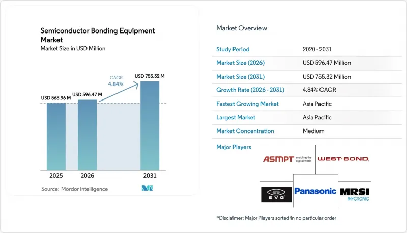
預計到 2026 年,半導體鍵合設備市場價值將達到 5.9647 億美元,高於 2025 年的 5.6896 億美元,預計到 2031 年將達到 7.5532 億美元。
預計從 2026 年到 2031 年,其複合年成長率將達到 4.84%。
需求成長反映了產業從平面小型化向垂直堆疊的轉變,在這一領域,異質整合策略需要精確的晶圓間和晶片間連接。領先的晶片製造商正在加速對先進封裝生產線的資本投資,以提高人工智慧加速器和高效能運算設備的頻寬、延遲和能源效率。隨著3奈米以下節點進入風險生產階段,混合銅-銅製程正在取代傳統的焊線,對準精度要求提高到10微米以下。同時,汽車電氣化和物聯網小型化正在擴大應用範圍,增加了永久性、臨時性和混合平台的累積訂單。然而,高昂的總擁有成本和更嚴格的揮發性有機化合物(VOC)環境法規增加了維持70%以上運轉率的壓力,促使買家協商全方位服務合約和預測性維護方案。
全球半導體鍵結設備市場趨勢及洞察
IDM 和代工廠的資本支出 (CAPEX) 增加
全球半導體製造設備投資預計將在2024年達到1,100億美元,並在2026年達到1,300億美元。光是台積電一家就已在2025年累計380億至420億美元用於設備升級,其中大部分資金將用於先進封裝和鍵結生產線。三星和英特爾的類似擴張凸顯了晶圓級整合對於支援高頻寬記憶體和晶片設計的巨大競爭需求。目前,資本投入主要集中在亞微米級光學對準模組、真空鍵結腔和人工智慧驅動的製程控制等領域。隨著裝置製造商為未來的設計變更做好準備,提供模組化升級方案的供應商正逐漸成為首選供應商。投資的增加透過縮短更換週期和擴大前端及後端晶圓廠的部署範圍,正在重振半導體鍵合設備市場。
汽車和物聯網設備中半導體使用量的激增
電動動力傳動系統、高級駕駛輔助系統 (ADAS) 和區域架構的普及將推動每輛車的半導體平均價值在 2024 年達到 950 美元。電動車車型採用碳化矽 (SiC) 和氮化鎵 (GaN) 功率裝置,需要高功率、高溫鍵合頭和強大的助焊劑管理系統。同時,物聯網穿戴式裝置和智慧家庭節點需要晶圓級晶片封裝,以縮小尺寸並延長電池壽命。這些多樣化的需求在設備層面趨於融合,要求可配置鍵合機能夠在高功率壓力曲線和精細的 MEMS 處理之間切換。供應商正在透過自適應夾具設計、卡盤平整度即時回饋和基於配方的壓力曲線來彌補這一差距。這一趨勢正在推動半導體鍵合設備市場出貨量的成長,同時也使汽車一級供應商和消費性電子原始設備製造商 (OEM) 的收入來源更加多元化。
擁有成本高,且總擁有成本 (TCO) 存在不確定性。
最先進的混合鍵合機售價超過300萬美元,但加上包括備件、耗材和校準在內的年度運行成本,其生命週期成本可能高達800萬美元。小規模OSAT(外包半導體組裝公司)在運轉率低於70%時會面臨困境,尤其是在家用電子電器淡季。藍圖的快速更新進一步加劇了財務建模的複雜性,因為即使是能夠處理10µm套刻精度的設備,也可能在短短兩個產品週期後就需要升級套件。儘管租賃方案、基於績效的服務合約和風險分擔定價模式正在興起,但財務總監仍然認為殘值不確定性是半導體鍵合設備市場新訂單的一大阻力。
細分市場分析
混合系統以5.88%的複合年成長率(CAGR)呈現最快成長,支持晶圓減薄和TSV(通孔向量)形成,並提供機械支撐所需的可逆黏附。混合系統同樣以5.88%的複合年成長率呈現最快成長,其目標是實現3nm或更小的整合,透過銅對銅直接連接最大限度地降低電阻和電遷移。預計到本十年末,混合平台半導體鍵合設備市場規模將從目前的小規模成長到與固定式設備相當的水平。製造商正透過兩級對準光學系統、主動調平卡盤和閉合迴路壓力控制等技術實現差異化,這些技術相結合可將貼片誤差控制在500nm以下。買家更傾向於能夠適應未來配方擴展的多模式設備,從而降低資本風險。這種轉變正在推動對能夠承受反覆熱循環而不發生分層的散熱材料以及軟性底部填充劑化學成分的積極研發。競爭也體現在產量上,目前,我們的旗艦機型透過平行夾臂和預測伺服調諧,承諾將循環時間縮短 20%。
這種轉變也導致設備更換週期延長。生產線經理在檢查老舊的共晶鍵合機時發現,維修成本每年成長12%。改用混合鍵合機無需二次工序,提高了車間利用率。然而,相關人員要求新設備與製造執行系統 (MES) 和工廠自動化層無縫整合,以實現晶片序號層級的可追溯性。供應商正透過整合 OPC-UA 閘道和邊緣分析功能,並將製程資料匯總到基於人工智慧的良率儀表板中來解決這個問題。這種生態系統相容性正在加速混合鍵合機在各工廠的部署,並提升其在半導體鍵合設備市場中的佔有率。
先進封裝仍將是核心細分市場,預計到2025年將佔銷售額的35.42%,主要得益於晶片處理器、高頻寬記憶體和高階智慧型手機SoC專案的支援。功率IC鍵結雖然不如先進封裝那樣引人注目,但其嚴格的空隙控制協議和高壓熱壓頭確保了穩定的產量。矽光電是一個成長快速的細分市場,複合年成長率高達5.73%。與開關ASIC共封裝的光引擎需要將鍺檢測器和III-V族雷射器以微米級精度放置在矽載片上,這就要求採用特殊的接合製程,並將溫升控制在250 度C以下。這種強勁的需求已經使矽光電在半導體鍵合設備整體市場的佔有率從個位數成長到兩位數。
MEMS感測器,尤其是用於汽車LiDAR和工業自動化的感測器,需要能夠承受高達1000次溫度波動的密封件。這種應力特性非常適合玻璃粉鍵合和陽極鍵合,從而維持了利基設備供應商的市場地位。 CMOS影像感測器正在追求更高的對準精度以確保光軸對準,這推動了對整合到鍵合頭中的先進自動對焦光學元件的訂單。同時,射頻元件引入了獨特的電阻,需要低損耗的佈線金屬,這影響了下一代設備的材料供應子系統。這種廣泛且新興的應用領域的整合保護了供應商免受市場波動的影響,並使半導體鍵合設備市場保持穩定的成長態勢。
區域分析
預計到2025年,亞太地區將佔全球銷售額的52.64%,主要得益於中國設備投資年增35%,達到496億美元。韓國緊隨其後,投資額為205億美元,而台灣地區儘管受到暫時性庫存調整的影響,仍貢獻了166億美元的銷售額。各地區的政策組合包括稅額扣抵、關稅豁免和基礎設施補貼,這些措施降低了混合鍵合機的實際採購價格,並鞏固了其在半導體鍵合設備市場的主導地位。台積電和三星等主要企業正在推動3D和混合技術的應用,提升了該地區的技術水平,並重新定義了精密卡盤和超平坦載片晶圓的供應鏈預期。
2024年,北美地區的銷售額達到137億美元,年增14%,主要得益於《晶片法案》(CHIPS Act)撥款,該法案旨在擴大國內產能。英特爾、德克薩斯德州儀器已宣佈在亞利桑那州、俄亥俄州和德克薩斯州開展多年封裝項目。雖然補貼獎勵策略正在加速訂單,但隨著津貼逐步減少,人們越來越擔心長期成本競爭力。然而,該地區具有靠近超大規模資料中心客戶的優勢,這些客戶正在尋求用於人工智慧工作負載的低延遲中介層,而人工智慧工作負載的低延遲中介層正在半導體鍵合設備市場創造對高價值混合鍵合機的需求。在歐洲,投資集中在德國和荷蘭,類比、電源和極紫外光微影設備供應商也集中於此。諸如IPCEI-ME/CT之類的聯合計畫正在將歐盟資金投入到汽車電源模組的3D整合技術中,這些模組對可靠性有著特別嚴格的要求。中東和非洲地區仍在發展中,但沙烏地阿拉伯的「2030願景」和阿拉伯聯合大公國的戰略技術基金正在為化合物半導體的試點生產線撥款。這些初步發展表明,半導體鍵合設備市場正在經歷更廣泛的區域多元化,並可能逐步擴展到傳統的亞太地區(APAC)之外。
其他好處:
- Excel格式的市場預測(ME)表
- 3個月的分析師支持
目錄
第1章:引言
- 研究假設和市場定義
- 調查範圍
第2章:調查方法
第3章執行摘要
第4章 市場狀況
- 市場概覽
- 市場促進因素
- IDM 和代工廠增加資本投資
- 汽車和物聯網設備中半導體使用量的激增
- 先進的2.5D/3D封裝平台的快速普及
- 政府主導的「CHIPS」補貼和稅收優惠
- CIS 和 3D-NAND 混合晶圓鍵結技術的商業化部署
- 用於人工智慧資料中心的矽光子中介層驅動晶圓鍵合技術設備
- 市場限制因素
- 擁有成本高,且總擁有成本 (TCO) 存在不確定性。
- 對準公差小於10µm的製程複雜性
- 超薄晶圓供應鏈瓶頸
- 加強揮發性有機化合物和黏合劑化學品的環境法規
- 產業價值鏈分析
- 監理情勢
- 技術展望
- 波特五力分析
- 供應商的議價能力
- 買方的議價能力
- 新進入者的威脅
- 替代品的威脅
- 競爭公司之間的競爭
- 宏觀經濟因素對市場的影響
第5章 市場規模與成長預測
- 透過裝置
- 永久黏合設備
- 臨時黏合裝置
- 混合鍵合設備
- 透過使用
- 先進包裝
- 功率積體電路與分離元件
- 光子裝置
- MEMS感測器和執行器
- 工程基板
- 射頻設備
- CMOS影像感測器
- 透過鍵合技術
- 熱壓黏接
- 共晶/焊點
- 黏合劑/聚合物黏合
- 超音波/熱超音波黏合
- 陽極鍵結/熔焊
- 按晶圓尺寸
- 200毫米或更小
- 200~300 mm
- 超過 300 毫米
- 最終用戶
- 整合設備製造商(IDM)
- 鑄造廠
- 半導體組裝和測試服務提供者(OSAT)
- 地區
- 北美洲
- 美國
- 北美其他地區
- 南美洲
- 歐洲
- 德國
- 法國
- 其他歐洲地區
- 亞太地區
- 中國
- 日本
- 韓國
- 印度
- 亞太其他地區
- 中東
- 非洲
- 北美洲
第6章 競爭情勢
- 市場集中度
- 策略趨勢
- 市佔率分析
- 公司簡介
- EV Group(EVG)
- ASMPT Semiconductor Solutions
- Mycronic AB(MRSI Systems)
- WestBond, Inc.
- Panasonic Holdings Corporation
- Palomar Technologies, Inc.
- Dr. Tresky AG
- BE Semiconductor Industries NV
- Fasford Technology Co., Ltd.
- Kulicke & Soffa Industries, Inc.
- DIAS Automation(HK)Ltd.
- Shibaura Mechatronics Corporation
- SUSS MicroTec SE
- Tokyo Electron Limited
- DISCO Corporation
- TOWA Corporation
- Hanmi Semiconductor Co., Ltd.
- Toray Engineering Co., Ltd.
- Hesse GmbH
- Finetech GmbH & Co. KG
第7章 市場機會與未來展望
The semiconductor bonding equipment market size in 2026 is estimated at USD 596.47 million, growing from 2025 value of USD 568.96 million with 2031 projections showing USD 755.32 million, growing at 4.84% CAGR over 2026-2031.
Demand growth mirrors the industry shift from planar scaling to vertical stacking, where heterogeneous integration strategies require precise wafer-to-wafer and die-to-wafer connections. Leading chipmakers have accelerated capital spending on advanced packaging lines to improve bandwidth, latency, and energy efficiency for AI accelerators and high-performance computing devices. Hybrid copper-to-copper processes are eclipsing conventional wire bonding as sub-3 nm nodes move into risk production, raising alignment-accuracy demands below 10 µm. At the same time, automotive electrification and IoT miniaturization widen the application footprint, expanding order books for permanent, temporary, and hybrid platforms. However, the high total cost of ownership and tighter environmental rules on volatile organic compounds add pressure to sustain utilization levels above 70%, prompting buyers to negotiate full-service contracts and predictive-maintenance packages.
Global Semiconductor Bonding Equipment Market Trends and Insights
Increasing CAPEX by IDMs and Foundries
Global semiconductor equipment spending hit USD 110 billion in 2024 and is on track for USD 130 billion by 2026. TSMC alone earmarked USD 38-42 billion for 2025 facility upgrades, a substantial portion of which funds advanced packaging and bonding lines. Comparable expansions by Samsung and Intel emphasize the competitive need for wafer-level integration that supports high-bandwidth memory and chiplet designs. Capital allocation now targets line items such as sub-micrometer optical alignment modules, vacuum bond chambers, and AI-enabled process control. Vendors that provide modular upgrade paths are gaining preferred-supplier status as device makers hedge against future design pivots. The investment uptick stimulates the semiconductor bonding equipment market by shortening replacement cycles and broadening the installed base across both front-end and back-end fabs.
Surging Semiconductor Content in Automotive and IoT Devices
Average semiconductor value per vehicle climbed to USD 950 in 2024, driven by electrified powertrains, advanced driver-assistance systems, and zonal architectures. Electric models specify silicon-carbide and gallium-nitride power devices that need high-force, high-temperature bonding heads and robust flux-management systems. In parallel, IoT wearables and smart home nodes demand wafer-level chip-scale packages that shrink footprint and extend battery life. These divergent requirements converge at the equipment level, where configurable bonders must toggle between high-power pressure profiles and delicate MEMS handling. Suppliers are addressing the gap with adaptive clamp designs, real-time chuck-planarity feedback, and recipe-driven force curves. The trend raises unit shipments in the semiconductor bonding equipment market while diversifying revenue streams across automotive Tier-1s and consumer OEMs.
High Cost of Ownership and TCO Uncertainty
State-of-the-art hybrid bonders list above USD 3 million, while annual running costs including spares, consumables, and calibration can lift lifetime spend to USD 8 million. Smaller OSATs struggle when utilization drifts below 70%, especially in consumer-electronics off-seasons. Rapid roadmap updates further complicate financial modeling because a tool qualified for 10 µm overlay may need retrofit kits after only two product cycles. Leasing programs, outcome-based service contracts, and shared-risk pricing models are emerging, yet CFOs still cite uncertain residual value as a brake on new orders within the semiconductor bonding equipment market.
Other drivers and restraints analyzed in the detailed report include:
- Rapid Adoption of Advanced 2.5D/3D Packaging Platforms
- Government-Backed "CHIPS" Subsidies and Tax Incentives
- Process Complexity at Sub-10 µm Alignment Tolerances
For complete list of drivers and restraints, kindly check the Table Of Contents.
Segment Analysis
Permanent bonders accounted for 38.74% of 2025 revenue, underpinned by their proven reliability in legacy device packaging. Temporary bonding tools cater to wafer thinning and TSV creation, providing the reversible adhesion needed for mechanical support. Hybrid systems register the quickest climb at 5.88% CAGR, targeting sub-3 nm integration where copper-to-copper direct attach minimizes resistance and electromigration. That growth lifts the semiconductor bonding equipment market size for hybrid platforms from a modest base toward parity with permanent tools before the decade closes. Manufacturers differentiate through dual-stage alignment optics, active levelling chucks, and closed-loop pressure control that collectively push placement error below 500 nm. Buyers favor multi-modal units that accept future recipe add-ons, lowering capital risk. The pivot intensifies R&D around heat-spreader materials and compliant under-fill chemistries that withstand repeated thermal cycles without delamination. Competition also hinges on throughput, with flagship machines now promising 20% cycle-time reductions achieved via parallel clamp arms and predictive servo tuning.
A broader equipment refresh cycle accompanies the shift. Line managers audited older eutectic stations and discovered maintenance outlays rising 12% per year. Swapping to hybrid bonders eliminates dual-pass processes, improving floor utilization. Yet stakeholders insist that new gear integrate seamlessly with MES and factory automation layers that handle traceability down to die serial number. Vendors respond by embedding OPC-UA gateways and edge analytics that channel process data into AI-based yield dashboards. Such ecosystem compatibility accelerates factory-wide adoption, reinforcing the hybrid segment's contribution to the semiconductor bonding equipment market.
Advanced packaging maintained 35.42% of 2025 revenue and remains the anchor segment, buttressed by chiplet processors, high-bandwidth memory, and premium smartphone SoC programs. Power IC bonding, while less glamorous, delivers stable volumes that depend on rigorous void-control protocols and high-pressure thermocompression heads. Silicon photonics is the standout high-velocity niche at a 5.73% CAGR. Optical engines co-packaged with switch ASICs need micron-accurate placement of germanium photodetectors and III-V lasers onto silicon carrier wafers, driving specialized bond recipes with controlled temperature ramps under 250 °C. The strong demand trajectory has already lifted the silicon-photonics slice from single digits toward a double-digit share of the overall semiconductor bonding equipment market size.
MEMS sensors, notably for automotive lidar and industrial automation, require hermetic seals that endure 1,000-cycle temperature swings. These stress profiles favor glass-frit or anodic bonding, sustaining a market foothold for niche tool vendors. CMOS image sensors push alignment fidelity to safeguard optical axis integrity, stoking orders for advanced auto-focus optics built into bond heads. RF devices, meanwhile, introduce unique impedances that compel low-loss interconnect metallurgy, influencing material-delivery subsystems on next-gen machines. The blend of widespread and emerging uses buffers suppliers from cyclical swings and keeps the semiconductor bonding equipment market on a stable growth path.
The Semiconductor Bonding Equipment Market Report is Segmented by Equipment Type (Permanent, Temporary, and Hybrid), Application (Advanced Packaging, Power IC and Discrete, and More), Bonding Technology (Thermocompression, Eutectic/Solder, and More), Wafer Size (<=200mm, and More), End User (IDMs, Foundries, and OSAT), and Geography (North America, Europe, and More). The Market Forecasts are Provided in Terms of Value (USD).
Geography Analysis
Asia-Pacific held 52.64% of 2025 revenue, underlined by USD 49.6 billion in equipment spending from China alone, up 35% year over year. South Korea followed with USD 20.5 billion, and Taiwan contributed USD 16.6 billion despite temporary inventory corrections. Regional policy packages include tax deductions, duty exemptions, and infrastructure subsidies that lower effective purchase prices of hybrid bonders, sustaining leadership in the semiconductor bonding equipment market. Local champions such as TSMC and Samsung spearhead 3D and hybrid adoption, elevating regional technical standards and reshaping supply-chain expectations for precision chucks and ultra-flat carrier wafers.
North America posted USD 13.7 billion in 2024 sales, advancing 14% alongside CHIPS Act allocations targeting domestic capacity expansion. Intel, Micron, and Texas Instruments have announced multiyear packaging projects anchored in Arizona, Ohio, and Texas. The subsidy stimulus accelerates inbound orders but raises concerns over long-term cost competitiveness once grants taper. Yet the region benefits from proximity to hyperscale-data-center customers demanding low-latency interposers for AI workloads, a segment that outlets more value-added hybrid bonders into the semiconductor bonding equipment market. Europe concentrates spending in Germany and the Netherlands where analog, power, and EUV tool vendors cluster. Collaborative programs like IPCEI-ME/CT channel EUR funding into 3D integration, especially for automotive power modules that require stringent reliability. Middle East and Africa remain nascent, though Saudi Arabia's Vision 2030 and the UAE's strategic tech funds have earmarked pilot lines for compound semiconductors. These early moves hint at wider regional diversification that could incrementally enlarge the semiconductor bonding equipment market beyond its traditional APAC stronghold.,
- EV Group (EVG)
- ASMPT Semiconductor Solutions
- Mycronic AB (MRSI Systems)
- WestBond, Inc.
- Panasonic Holdings Corporation
- Palomar Technologies, Inc.
- Dr. Tresky AG
- BE Semiconductor Industries N.V.
- Fasford Technology Co., Ltd.
- Kulicke & Soffa Industries, Inc.
- DIAS Automation (HK) Ltd.
- Shibaura Mechatronics Corporation
- SUSS MicroTec SE
- Tokyo Electron Limited
- DISCO Corporation
- TOWA Corporation
- Hanmi Semiconductor Co., Ltd.
- Toray Engineering Co., Ltd.
- Hesse GmbH
- Finetech GmbH & Co. KG
Additional Benefits:
- The market estimate (ME) sheet in Excel format
- 3 months of analyst support
TABLE OF CONTENTS
1 INTRODUCTION
- 1.1 Study Assumptions and Market Definition
- 1.2 Scope of the Study
2 RESEARCH METHODOLOGY
3 EXECUTIVE SUMMARY
4 MARKET LANDSCAPE
- 4.1 Market Overview
- 4.2 Market Drivers
- 4.2.1 Increasing CAPEX by IDMs and foundries
- 4.2.2 Surging semiconductor content in automotive and IoT devices
- 4.2.3 Rapid adoption of advanced 2.5D/3D packaging platforms
- 4.2.4 Government-backed "CHIPS" subsidies and tax incentives
- 4.2.5 Commercial roll-out of hybrid wafer-to-wafer bonding in CIS and 3D-NAND
- 4.2.6 Silicon-photonic interposers for AI datacenters driving wafer bonding tools
- 4.3 Market Restraints
- 4.3.1 High cost of ownership and TCO uncertainty
- 4.3.2 Process complexity at sub-10 µm alignment tolerances
- 4.3.3 Supply-chain bottlenecks for ultra-flat carrier wafers
- 4.3.4 Stricter VOC / adhesive-chemistry environmental regulations
- 4.4 Industry Value Chain Analysis
- 4.5 Regulatory Landscape
- 4.6 Technological Outlook
- 4.7 Porter's Five Forces Analysis
- 4.7.1 Bargaining Power of Suppliers
- 4.7.2 Bargaining Power of Buyers
- 4.7.3 Threat of New Entrants
- 4.7.4 Threat of Substitutes
- 4.7.5 Intensity of Competitive Rivalry
- 4.8 Impact of Macroeconomic Factors on the Market
5 MARKET SIZE AND GROWTH FORECASTS (VALUE)
- 5.1 By Equipment Type
- 5.1.1 Permanent Bonding Equipment
- 5.1.2 Temporary Bonding Equipment
- 5.1.3 Hybrid Bonding Equipment
- 5.2 By Application
- 5.2.1 Advanced Packaging
- 5.2.2 Power IC and Discrete
- 5.2.3 Photonic Devices
- 5.2.4 MEMS Sensors and Actuators
- 5.2.5 Engineered Substrates
- 5.2.6 RF Devices
- 5.2.7 CMOS Image Sensors
- 5.3 By Bonding Technology
- 5.3.1 Thermocompression Bonding
- 5.3.2 Eutectic/Solder Bonding
- 5.3.3 Adhesive/Polymer Bonding
- 5.3.4 Ultrasonic / Thermosonic Bonding
- 5.3.5 Anodic / Fusion Bonding
- 5.4 By Wafer Size
- 5.4.1 Less than equal to 200 mm
- 5.4.2 200-300 mm
- 5.4.3 Greater than 300 mm
- 5.5 By End User
- 5.5.1 Integrated Device Manufacturers (IDMs)
- 5.5.2 Foundries
- 5.5.3 Outsourced Semiconductor Assembly and Test (OSAT)
- 5.6 Geography
- 5.6.1 North America
- 5.6.1.1 United States
- 5.6.1.2 Rest of North America
- 5.6.2 South America
- 5.6.3 Europe
- 5.6.3.1 Germany
- 5.6.3.2 France
- 5.6.3.3 Rest of Europe
- 5.6.4 Asia-Pacific
- 5.6.4.1 China
- 5.6.4.2 Japan
- 5.6.4.3 South Korea
- 5.6.4.4 India
- 5.6.4.5 Rest of Asia-Pacific
- 5.6.5 Middle East
- 5.6.6 Africa
- 5.6.1 North America
6 COMPETITIVE LANDSCAPE
- 6.1 Market Concentration
- 6.2 Strategic Moves
- 6.3 Market Share Analysis
- 6.4 Company Profiles (includes Global level Overview, Market level overview, Core Segments, Financials as available, Strategic Information, Market Rank/Share for key companies, Products and Services, and Recent Developments)
- 6.4.1 EV Group (EVG)
- 6.4.2 ASMPT Semiconductor Solutions
- 6.4.3 Mycronic AB (MRSI Systems)
- 6.4.4 WestBond, Inc.
- 6.4.5 Panasonic Holdings Corporation
- 6.4.6 Palomar Technologies, Inc.
- 6.4.7 Dr. Tresky AG
- 6.4.8 BE Semiconductor Industries N.V.
- 6.4.9 Fasford Technology Co., Ltd.
- 6.4.10 Kulicke & Soffa Industries, Inc.
- 6.4.11 DIAS Automation (HK) Ltd.
- 6.4.12 Shibaura Mechatronics Corporation
- 6.4.13 SUSS MicroTec SE
- 6.4.14 Tokyo Electron Limited
- 6.4.15 DISCO Corporation
- 6.4.16 TOWA Corporation
- 6.4.17 Hanmi Semiconductor Co., Ltd.
- 6.4.18 Toray Engineering Co., Ltd.
- 6.4.19 Hesse GmbH
- 6.4.20 Finetech GmbH & Co. KG
7 MARKET OPPORTUNITIES AND FUTURE OUTLOOK
- 7.1 White-space and Unmet-need Assessment
 半導體晶圓鍵合技術市場分析及預測至 2035 年:按類型、產品類型、技術、應用、材料類型、製程、最終用戶、設備和解決方案分類。
 半導體鍵合市場:2026-2032年全球市場預測(依設備類型、鍵結方法、封裝結構、基板材料、應用、最終用戶和產業分類)半導體鍵結市場分析及預測(至2035年):類型、產品、技術、應用、材料類型、裝置、製程、最終用戶、設備、解決方案
 半導體鍵結市場規模、佔有率、成長及全球產業分析:依類型、應用和地區劃分的洞察與預測(2026-2034年)
 半導體鍵結市場-全球產業規模、佔有率、趨勢、機會與預測:按類型、製程類型、鍵結技術、應用、地區和競爭格局分類,2021-2031年
 半導體鍵合市場,按鍵合技術、鍵結材料、最終用戶和地區分類
 全球混合鍵結市場按封裝架構、設備類型和整合度分類-預測至2032年
 TCB鍵合機:全球市佔率排名、總銷售額與需求預測(2025-2031年)
 全球半導體鍵結市場混合鍵合技術市場(按技術、基板材料、最終用戶產業和應用分類)- 2025 年至 2030 年全球預測