


 |
市場調查報告書
商品編碼
2035097
面板級包裝:市場佔有率分析、產業趨勢與統計、成長預測(2026-2031 年)Panel Level Packaging - Market Share Analysis, Industry Trends & Statistics, Growth Forecasts (2026 - 2031) |
||||||
※ 本網頁內容可能與最新版本有所差異。詳細情況請與我們聯繫。
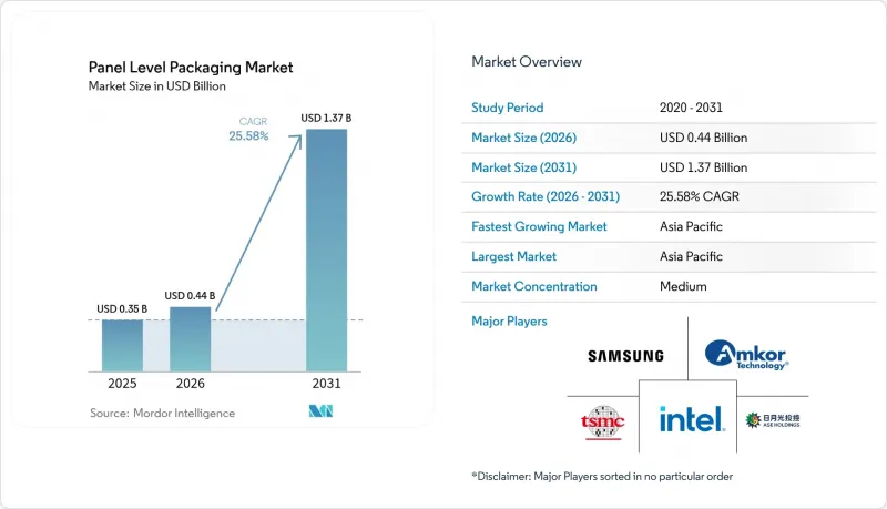
預計面板級包裝市場將從 2025 年的 3.5 億美元成長到 2026 年的 4.4 億美元,到 2031 年將達到 13.7 億美元,2026 年至 2031 年的複合年成長率為 25.58%。
這種快速成長軌跡反映了半導體產業從以晶圓為中心轉向以面板為中心的架構轉變,這一轉變實現了規模經濟,並滿足了人工智慧和高效能運算的激增需求。面板格式在多晶片設計中可實現高達 40% 的基板利用率提升,從而緩解了邏輯和儲存節點小型化至 5 奈米以下時的成本壓力。基板創新,特別是向玻璃芯的轉變,有望實現更精確的尺寸控制和更高的熱穩定性,從而支持不斷增加的輸入輸出數量。設備供應商正在積極回應,推出能夠實現 10 微米以下微結構的 600 毫米 × 600 毫米微影術系統,突破了傳統解析度的限制,並擴大了下一代整合技術的目標市場。供應鏈合作也不斷加強,這體現在主要代工廠的垂直整合策略以及代工廠與 OSAT 合作夥伴之間的合作產能擴張。
全球面板級包裝市場趨勢及洞察
成本降低與晶圓級封裝的比較
轉向面板封裝形式可將多晶片設計中的基板利用率提高高達 40%,即使考慮到昂貴的模具成本,也能降低單位成本。日月光 (ASE) 投資 2 億美元建設 310mm x 310mm 生產線,表明其致力於擴大生產規模,為大規模生產的消費電子產品提供所需的晶圓開片數量,從而在產品較短的生命週期內攤銷模具成本。亞洲契約製造製造商透過將基板製造、線路重布(RDL) 處理和最終測試整合到同一園區內,獲得了更多優勢並降低了物流成本。產量較低的西方製造商則面臨更陡峭的成本曲線,競爭差距也日益擴大。因此,面板優先策略在承包封裝競標中越來越起訂單作用。
人工智慧/高效能運算晶片需求激增
大規模語言模型推理和訓練環境對GPU叢集密度的需求比以往任何時候都更高,這推動了向更大尺寸、無中介層的封裝的轉變,以保持頻寬。台積電的CoWoS(晶片封裝於基板面板之上)藍圖計劃於2027年開始試生產,該路線圖將在保持恆定熱阻的同時,將CoWoS的掩模尺寸擴大一倍。到2026年,代工廠正以每年超過60%的速度擴大CoWoS的產能,但高頻寬記憶體(HBM)生產線的訂單預計仍然存在,這將迫使一級客戶考慮下一代加速卡在面板級封裝市場上的替代方案。能夠展示面板級封裝中超過20kW的貨架級散熱能力的領先公司將最有希望獲得多年供貨合約。
高昂的資本投資成本和翹曲問題
一條600毫米生產線運作運轉需要超過5億美元的沉積、圖形化和測量設備投資。面板基板在熱負荷下會膨脹,若不進行補償,翹曲度可超過2毫米。 SK Key Foundry和LB Semicon的Direct-RDL製程透過在固化過程中固定面板邊緣來抑制翹曲,但這種設備改造會使工具成本增加15%。小規模的OSAT(外包半導體組裝公司)難以資金籌措這些升級費用,阻礙了全球供應的擴張。在低模量介電材料和主動式翹曲校正卡盤實現實用化之前,良率降低仍將是短期內進軍面板級封裝市場的一大障礙。
細分市場分析
到2025年,扇出型面板級封裝將佔銷售額的44.60%,成為消費性電子和行動裝置的旗艦產品,滿足中等I/O密度的需求。預計到2031年,該細分市場的面板級封裝規模將達到1.6億美元,並以19.80%的年均成長率成長。領先的OSAT(外包半導體工廠任務)廠商正利用成熟的晶片面朝下(DFD)製程實現超過97%的良率,每月晶圓產量超過2萬片,成本比晶圓扇出封裝方法低兩位數百分比。然而,頻寬密集型加速器正在突破該方法的焊盤間距極限,促使創新者轉向2.5D/3D面板解決方案。
2.5D/3D面板整合在2025年僅佔總營收的19.10%,但卻是成長最快的細分市場,複合年成長率高達29.20%。異質堆疊技術透過將運算、儲存和類比晶片排列在被動式玻璃基板上,可將互連長度縮短高達70%。早期商業化應用主要集中在人工智慧推理卡上,每個封裝包含16個或更多晶片。隨著2.5D/3D技術走出資料中心的小眾市場,並滲透到汽車網域控制器領域,預計2031年,其在面板級封裝領域的市佔率將達到31.80%。
有機層壓板受益於低成本樹脂體系和成熟的供應鏈,預計2025年將維持56.10%的市場佔有率,市場規模達到2億美元。然而,該細分市場的複合年成長率僅20.40%,落後於整體面板級封裝市場。這反映了層數的物理限制以及熱膨脹係數(CTE)的不匹配。相較之下,去年市佔率僅12.30%的玻璃芯材預計到2031年將以28.90%的複合年成長率成長。三星的H玻璃藍圖旨在2026年實現量產,尺寸漂移控制在0.3 ppm/ 度C(僅為有機材料的十分之一),並可實現線寬小於5µm的線路重布。矽和模塑重建面板仍屬於小眾產品,主要用於高功率或超低成本應用。
區域分析
預計到2025年,亞太地區將佔全球銷售額的69.20%,並將繼續以27.60%的複合年成長率(CAGR)推動面板級封裝市場的發展,直至2031年。中國正透過政府獎勵投資面板封裝生產線,以配合國家人工智慧晶片計畫;日本的資本投資在2024年成長了82%,達到70億美元,以支持其國內製程能力的提升。韓國正在推動玻璃芯基板的研發,而台灣的台積電則在推廣一體化代工封裝流程,將CoWoS、CoPoS和測試整合到一個晶圓廠叢集中。
北美地區也緊追在後,主要得益於《晶片封裝和整合法案》(CHIPS Act)撥出的16億美元資金,用於先進封裝技術的發展。安姆科(Amcor)位於亞利桑那州、投資4億美元的工廠將於2026年運作,該工廠與台積電(TSMC)新建的Fab 21工廠位置同一廠址,將縮短美國客戶的生產週期。同樣,SK海力士(SK Hynix)也已在印第安納州撥款4.5億美元用於HBM封裝技術,這表明各州都在積極吸引高附加價值後端企業。
儘管歐洲的市場佔有率仍維持在個位數,但對國內生產的擔憂正推動當地契約製造(OSAT)公司的建立,從而帶動其市場佔有率的上升趨勢。富士康和泰雷茲決定投資2.5億歐元,為航太和國防領域新建一座扇出型半導體製造廠。同時,英飛凌正與安姆科合作,擴大在葡萄牙的面板產能,該計畫計劃於2025年中期運作。中東、非洲和南美洲目前仍主要由消費主導,組裝基地有限,但沙烏地阿拉伯和巴西的獎勵計畫可能會在本十年後半期改變這種局面。
其他好處:
- Excel格式的市場預測(ME)表
- 3個月的分析師支持
目錄
第1章:引言
- 市場分析與定義的前提條件
- 分析範圍
第2章 分析方法
第3章執行摘要
第4章 市場狀況
- 市場概覽
- 市場促進因素
- 降低成本和晶圓層次電子構裝
- 人工智慧/高效能運算晶片需求激增
- 5G/6G和邊緣設備的普及
- 採用尼康 600 x 600 毫米數位微影術。
- 2026年起過渡到玻璃芯基板
- 歐盟和美國關於先進包裝的回流補貼
- 市場限制因素
- 高資本密集度和扭曲問題
- 製程整合複雜度超過 300 毫米
- 大尺寸面板中亞微米級微影術的良率急劇下降。
- ABF-GCP介電薄膜供應瓶頸
- 產業價值鏈分析
- 監理情勢
- 技術展望
- 波特五力分析
- 供應商議價能力
- 買方的議價能力
- 新進入者的威脅
- 替代品的威脅
- 競爭公司之間的競爭關係
第5章 市場規模與成長預測
- 產品技術
- 扇出型面板級封裝(FOPLP)
- 嵌入式橋接器(eBridge)
- 2.5D/3D面板整合
- 扇入式面板級封裝
- 按基板
- 有機層壓
- 玻璃芯
- 矽
- 模製和重新配置的面板
- 按面板尺寸
- 300 毫米 × 300 毫米或更小
- 301-510 毫米 × 510 毫米
- 511 毫米 × 600 毫米或更大
- 透過工業應用
- 家用電子電器
- 汽車(ADAS、電動車電源)
- 通訊(5G/6G基礎設施)
- 航太/國防
- 工業物聯網
- 按地區
- 北美洲
- 美國
- 加拿大
- 墨西哥
- 南美洲
- 巴西
- 阿根廷
- 南美洲其他地區
- 歐洲
- 德國
- 英國
- 法國
- 義大利
- 其他歐洲國家
- 亞太地區
- 中國
- 日本
- 韓國
- 印度
- 亞太其他地區
- 中東
- 沙烏地阿拉伯
- 阿拉伯聯合大公國
- 其他中東國家
- 非洲
- 南非
- 其他非洲地區
- 北美洲
第6章 競爭情勢
- 市場集中度
- 策略趨勢
- 市佔率分析
- 公司簡介
- Samsung Electronics Co., Ltd.
- Taiwan Semiconductor Manufacturing Company Limited(TSMC)
- Intel Corporation
- ASE Technology Holding Co., Ltd.
- Amkor Technology, Inc.
- Powertech Technology Inc.
- Nepes Corporation
- Unimicron Technology Corp.
- DECA Technologies, Inc.
- JCET Group Co., Ltd.
- Fraunhofer Institute for Reliability and Microintegration IZM
- Nikon Corporation
- Ajinomoto Fine-Techno Co., Inc.
- Shinko Electric Industries Co., Ltd.
- LG Innotek Co., Ltd.
- K&S(Kulicke & Soffa Industries, Inc.)
- Veeco Instruments Inc.
- Applied Materials, Inc.
- Ultratech(Veeco)
- Tokyo Electron Limited
- Brewer Science, Inc.
第7章 市場機會與未來展望
The panel-level packaging market size is expected to grow from USD 0.35 billion in 2025 to USD 0.44 billion in 2026 and is forecast to reach USD 1.37 billion by 2031 at 25.58% CAGR over 2026-2031.
The steep trajectory mirrors the semiconductor sector's shift from wafer-centric to panel-centric architectures, a move that unlocks scale advantages and aligns with burgeoning AI and high-performance computing demand. Panel formats deliver up to 40% better substrate utilization for multi-die designs, easing cost pressure as logic and memory nodes scale below 5 nm. Substrate innovation, notably the transition toward glass cores, promises tighter dimensional control and improved thermal stability, which together support rising input/output counts. Equipment vendors have responded with 600 mm X 600 mm lithography systems capable of sub-10 µm features, erasing a former resolution ceiling and widening the addressable market for next-generation integration. Supply-chain coordination is intensifying, illustrated by vertically integrated strategies from leading foundries and by cooperative capacity expansions between foundry and OSAT partners.
Global Panel Level Packaging Market Trends and Insights
Cost Reduction Versus Wafer-Level Packaging
Moving to panel formats yields up to 40% better substrate utilization for multi-die designs, cutting cost per placement even after accounting for expensive tooling. ASE's USD 200 million investment in 310 mm X 310 mm lines signals a commitment to volume scaling, and high-volume consumer devices supply the wafer starts needed to amortize tools across short life cycles. Asian contract manufacturers gain further leverage by clustering substrate fabrication, redistribution-layer processing, and final test inside single campuses, reducing logistics overhead. Western houses with lower volumes face a steeper cost curve, widening the competitiveness gap. As a result, panel-first strategies increasingly determine win rates in turnkey package bids.
Surge of AI/HPC Chip Demand
Large language-model inference and training floors require ever-denser GPU clusters, driving packaging toward larger interposer-free footprints that sustain bandwidth. TSMC's Chip-on-Panel-on-Substrate (CoPoS) roadmap, slated for 2027 risk production, doubles reticle-limited dimensions of CoWoS while holding thermal resistance steady. The foundry is expanding CoWoS capacity more than 60% annually through 2026, yet still projects backlog in high-bandwidth memory (HBM) lines, pushing Tier-1 customers to evaluate panel-level packaging market alternatives for next-generation accelerator cards. Early movers able to demonstrate >20 kW shelf-level cooling in panel packages are best positioned to secure multi-year supply agreements.
High Capital Intensity and Warpage Issues
A full 600 mm line demands more than USD 500 million in deposition, patterning, and metrology gear. Panel substrates expand under thermal load, generating a bow that can exceed 2 mm if not compensated. SK Key Foundry and LB Semicon's Direct-RDL flow clamps panel edges during cure to limit deflection, but equipment retrofits add 15% to tool cost. Smaller OSATs struggle to finance those upgrades, constraining global supply expansion. Until low-modulus dielectrics or active warp-compensation chucks mature, yield drag remains a check on near-term penetration of the panel-level packaging market.
Other drivers and restraints analyzed in the detailed report include:
- Proliferation of 5G/6G and Edge Devices
- Nikon 600 X 600 mm digital lithography adoption
- Process-Integration Complexity Beyond 300 mm
For complete list of drivers and restraints, kindly check the Table Of Contents.
Segment Analysis
Fan-Out Panel Level Packaging commanded 44.60% of 2025 revenue, making it the workhorse for consumer and mobile devices where moderate I/O density is sufficient. The panel-level packaging market size for this segment reached USD 0.16 billion and is projected to grow at 19.80% through 2031. Large OSATs leverage mature die-face-down flows to drive yields above 97%, beating wafer fan-out costs by double-digit margins on runs above 20,000 panels per month. Nevertheless, bandwidth-hungry accelerators are stretching the approach's pad pitch limits, pressing innovators toward 2.5D/3D panel solutions.
2.5D/3D panel integration, while holding only 19.10% of 2025 sales, is the fastest mover at a 29.20% CAGR. Heterogeneous stacking places compute, memory, and analog tiles on passive glass carriers, cutting interconnect length by up to 70%. Early commercial wins center on AI inference cards where a single package hosts >16 chiplets. The panel-level packaging market share for 2.5D/3D approaches is expected to hit 31.80% by 2031 as the technique escapes datacenter niches and filters into automotive domain controllers.
Organic laminate retained a 56.10% share in 2025, valued at USD 0.20 billion, benefiting from low-cost resin systems and entrenched supply chains. However, the segment's 20.40% CAGR lags the overall panel-level packaging market, reflecting physical limits on layer count and CTE mismatch. Glass cores, in contrast, posted only an 12.30% share last year but will grow at a 28.90% CAGR to 2031. Samsung's H-glass roadmap targets volume ramp in 2026, offering 0.3 ppm/°C dimensional drift, one-tenth that of organics, unlocking sub-5 µm line-width redistribution layers. Silicon and molded reconstituted panels remain niche, serving high-power or ultra-low-cost corners.
The Panel Level Packaging Market Report is Segmented by Packaging Technology (Fan-Out Panel Level Packaging, Embedded Bridge, and More), Substrate Material (Organic Laminate, Glass Core, and More), Panel Size (<=300mmX300mm, 301-510mmX510mm, >=511mmX600mm), Industry Application (Consumer Electronics, Automotive, and More), and Geography (North America, Europe, and More). The Market Forecasts are Provided in Terms of Value (USD).
Geography Analysis
Asia-Pacific captured 69.20% of 2025 revenue and continues to lead the panel-level packaging market at a 27.60% CAGR through 2031. China funnels state incentives toward panel packaging lines aligned with sovereign AI chip programs, and Japan's equipment outlays rose 82% in 2024 to USD 7 billion, underpinning domestic process capability. South Korea advances glass-core substrates, while Taiwan's TSMC pushes integrated foundry-packaging flows that bundle CoWoS, CoPoS, and testing in a single fab cluster.
North America follows, anchored by CHIPS-Act funding of USD 1.6 billion earmarked for advanced packaging. Amkor's USD 400 million Arizona plant comes online in 2026, co-located with TSMC's new Fab 21 to shorten cycle times for U.S. customers. SK Hynix likewise has earmarked USD 450 million for HBM packaging in Indiana, demonstrating that states are bidding aggressively for high-value backend operations.
Europe's share remains single-digit but is rising as sovereignty concerns spur local OSAT formation. Foxconn and Thales committed EUR 250 million to a new fan-out facility aimed at aerospace and defense, while Infineon partnered with Amkor to add panel capacity in Portugal that comes online mid-2025. Middle East and Africa and South America remain consumption-centric, with limited assembly footprints yet, though incentive schemes in Saudi Arabia and Brazil could shift that balance later in the decade.
- Samsung Electronics Co., Ltd.
- Taiwan Semiconductor Manufacturing Company Limited (TSMC)
- Intel Corporation
- ASE Technology Holding Co., Ltd.
- Amkor Technology, Inc.
- Powertech Technology Inc.
- Nepes Corporation
- Unimicron Technology Corp.
- DECA Technologies, Inc.
- JCET Group Co., Ltd.
- Fraunhofer Institute for Reliability and Microintegration IZM
- Nikon Corporation
- Ajinomoto Fine-Techno Co., Inc.
- Shinko Electric Industries Co., Ltd.
- LG Innotek Co., Ltd.
- K&S (Kulicke & Soffa Industries, Inc.)
- Veeco Instruments Inc.
- Applied Materials, Inc.
- Ultratech (Veeco)
- Tokyo Electron Limited
- Brewer Science, Inc.
Additional Benefits:
- The market estimate (ME) sheet in Excel format
- 3 months of analyst support
TABLE OF CONTENTS
1 Introduction
- 1.1 Study Assumptions and Market Definition
- 1.2 Scope of the Study
2 Research Methodology
3 Executive Summary
4 Market Landscape
- 4.1 Market Overview
- 4.2 Market Drivers
- 4.2.1 Cost reduction versus wafer-level packaging
- 4.2.2 Surge of AI/HPC chip demand
- 4.2.3 Proliferation of 5G/6G and edge devices
- 4.2.4 Nikon 600 x 600 mm digital lithography adoption
- 4.2.5 Shift to glass-core substrates >=2026
- 4.2.6 EU/US reshoring subsidies tied to advanced packaging
- 4.3 Market Restraints
- 4.3.1 High capital intensity and warpage issues
- 4.3.2 Process-integration complexity beyond 300 mm
- 4.3.3 Sub-1 µm lithography yield cliff on large panels
- 4.3.4 Supply bottleneck for ABF-GCP dielectric films
- 4.4 Industry Value Chain Analysis
- 4.5 Regulatory Landscape
- 4.6 Technological Outlook
- 4.7 Porter's Five Forces Analysis
- 4.7.1 Bargaining Power of Suppliers
- 4.7.2 Bargaining Power of Buyers
- 4.7.3 Threat of New Entrants
- 4.7.4 Threat of Substitutes
- 4.7.5 Intensity of Rivalry
5 Market Size and Growth Forecasts (Value)
- 5.1 By Packaging Technology
- 5.1.1 Fan-Out Panel Level Packaging (FOPLP)
- 5.1.2 Embedded Bridge (eBridge)
- 5.1.3 2.5D/3D Panel Integration
- 5.1.4 Fan-In Panel Level Packaging
- 5.2 By Substrate Material
- 5.2.1 Organic Laminate
- 5.2.2 Glass Core
- 5.2.3 Silicon
- 5.2.4 Molded Reconstituted Panel
- 5.3 By Panel Size
- 5.3.1 <=300 mm X 300 mm
- 5.3.2 301 - 510 mm X 510 mm
- 5.3.3 >=511 mm X 600 mm
- 5.4 By Industry Application
- 5.4.1 Consumer Electronics
- 5.4.2 Automotive (ADAS, EV Power)
- 5.4.3 Telecommunications (5G/6G Infrastructure)
- 5.4.4 Aerospace and Defense
- 5.4.5 Industrial and IoT
- 5.5 By Geography
- 5.5.1 North America
- 5.5.1.1 United States
- 5.5.1.2 Canada
- 5.5.1.3 Mexico
- 5.5.2 South America
- 5.5.2.1 Brazil
- 5.5.2.2 Argentina
- 5.5.2.3 Rest of South America
- 5.5.3 Europe
- 5.5.3.1 Germany
- 5.5.3.2 United Kingdom
- 5.5.3.3 France
- 5.5.3.4 Italy
- 5.5.3.5 Rest of Europe
- 5.5.4 Asia-Pacific
- 5.5.4.1 China
- 5.5.4.2 Japan
- 5.5.4.3 South Korea
- 5.5.4.4 India
- 5.5.4.5 Rest of Asia-Pacific
- 5.5.5 Middle East
- 5.5.5.1 Saudi Arabia
- 5.5.5.2 United Arab Emirates
- 5.5.5.3 Rest of Middle East
- 5.5.6 Africa
- 5.5.6.1 South Africa
- 5.5.6.2 Rest of Africa
- 5.5.1 North America
6 Competitive Landscape
- 6.1 Market Concentration
- 6.2 Strategic Moves
- 6.3 Market Share Analysis
- 6.4 Company Profiles (includes Global level Overview, Market level overview, Core Segments, Financials as available, Strategic Information, Market Rank/Share for key companies, Products and Services, and Recent Developments)
- 6.4.1 Samsung Electronics Co., Ltd.
- 6.4.2 Taiwan Semiconductor Manufacturing Company Limited (TSMC)
- 6.4.3 Intel Corporation
- 6.4.4 ASE Technology Holding Co., Ltd.
- 6.4.5 Amkor Technology, Inc.
- 6.4.6 Powertech Technology Inc.
- 6.4.7 Nepes Corporation
- 6.4.8 Unimicron Technology Corp.
- 6.4.9 DECA Technologies, Inc.
- 6.4.10 JCET Group Co., Ltd.
- 6.4.11 Fraunhofer Institute for Reliability and Microintegration IZM
- 6.4.12 Nikon Corporation
- 6.4.13 Ajinomoto Fine-Techno Co., Inc.
- 6.4.14 Shinko Electric Industries Co., Ltd.
- 6.4.15 LG Innotek Co., Ltd.
- 6.4.16 K&S (Kulicke & Soffa Industries, Inc.)
- 6.4.17 Veeco Instruments Inc.
- 6.4.18 Applied Materials, Inc.
- 6.4.19 Ultratech (Veeco)
- 6.4.20 Tokyo Electron Limited
- 6.4.21 Brewer Science, Inc.
7 Market Opportunities and Future Outlook
- 7.1 White-space and Unmet-need Assessment

