


 |
市場調查報告書
商品編碼
1687765
半導體蝕刻設備:市場佔有率分析、行業趨勢和統計、成長預測(2025-2030 年)Semiconductor Etch Equipment - Market Share Analysis, Industry Trends & Statistics, Growth Forecasts (2025 - 2030) |
||||||
※ 本網頁內容可能與最新版本有所差異。詳細情況請與我們聯繫。
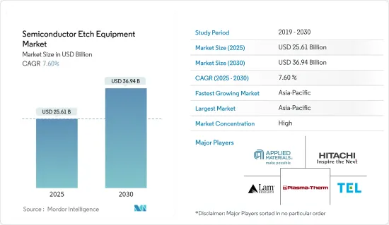
預計半導體蝕刻設備市場規模在 2025 年將達到 256.1 億美元,在 2030 年將達到 369.4 億美元,預測期內(2025-2030 年)的複合年成長率為 7.6%。
主要亮點
- 資本投資推動半導體蝕刻設備的成長:由於半導體加工的資本投資增加,半導體蝕刻設備市場正在經歷強勁成長。全球對半導體產業的投資正在激增,其中法國投資19億美元,德國投資120億美元用於微電子計劃。美國公司佔據市場主導地位,控制主要製造製程設備類別的50%以上,而日本則佔了光阻劑加工市場的90%。投資激增推動了對生產更小、更薄、更快的設備至關重要的先進蝕刻技術的需求。
- 中國投資:中國宣布計劃在 2020 年至 2025 年期間投資 1.4 兆美元,重點投資包括半導體在內的先進技術。
- 在日本聯合投資:台積電和索尼公司共同投資70億美元在日本新建晶片工廠。
- 歐盟重點關注數位基礎設施:歐盟已將其 9,170 億美元新冠疫情復甦基金中的 20% 分配給數位基礎設施,重點是微電子技術。
- 英特爾的巨額投資:英特爾宣布計劃在歐洲投資 880 億美元,包括在德國建立一個新的大型晶圓廠。
- 技術進步重塑市場格局:快速的技術進步正在重塑半導體蝕刻設備市場,明顯轉向消費量更少化學品且更適合自動化晶圓廠製造的電漿蝕刻系統。這種演變是由對更節能和更高性能電子設備日益成長的需求所驅動,從而刺激了小型化半導體積體電路 (IC) 的發展。
- 選擇性蝕刻:2022 年 2 月,Lam Research 宣布推出一款選擇性蝕刻設備,該設備採用創新的晶圓製造技術,用於全柵 (GAA) 電晶體架構。
- 表面處理技術:ClassOne Technology 於 2022 年 7 月在其 Solstice 自動化單晶圓平台中擴展了表面處理 (SP) 技術。
- 熱處理創新:Plasma-Therm 憑藉其 Heatpulse 快速熱處理 (RTP) 平台進行創新,贏得了全球晶片製造商的多項採購。
- FPD設備開發:我們正在開發能夠處理電視、智慧型手機和其他設備的高解析度和低耗電量的FPD製造設備。
- 反映多種應用的市場細分:半導體蝕刻設備市場根據產品類型、蝕刻膜類型和應用進行細分。高密度蝕刻設備引領市場,預計到 2027 年營收將達到 192.8961 億美元。預計導體蝕刻部分在 2022 年至 2027 年期間的複合年成長率為 4.55%,到預測期結束時將達到 125.5446 億美元。
- 關鍵促進因素:鑄造、MEMS、感測器和電力設備是推動市場成長的主要應用領域。
- 智慧型設備和物聯網:物聯網的採用和對智慧設備日益成長的需求正在推動半導體小型化的需求,從而刺激蝕刻設備市場的發展。
- 太陽能電池濕蝕刻:濕蝕刻因其高選擇性和材料保存特性,在太陽能電池製造中不斷被應用。
- 投資分析凸顯市場潛力:半導體蝕刻設備市場正在進行大量投資,反映了其成長潛力。各公司正在擴大製造能力並加強研發力度,以滿足對先進半導體技術日益成長的需求。
- Lam Research 擴張:Lam Research 於 2021 年 8 月在馬來西亞開設了最大的工廠,加強了其全球製造地。
- 美國半導體投資:美國政府核准對半導體產業投資500億美元,重點投資生產、研究和設計。
- 印度的半導體推動:印度已決定在半導體製造業投資 100 億美元,並計劃建立各種製造工廠。
- MIT.nano 擴大研發:2021 年 7 月,MIT.nano 收購了新的 SAMCO感應耦合電漿(ICP) 反應離子刻蝕 (RIE) 工具,以加強對新材料的研究。
半導體蝕刻設備市場趨勢
高密度蝕刻設備領域佔主要市場佔有率
- 主導市場佔有率和強勁成長:高密度蝕刻設備領域佔最大的市場佔有率,佔2021年半導體蝕刻設備市場的63.59%,達到125.441億美元。預計到 2027 年,該領域規模將成長至 192.896 億美元,複合年成長率為 5.66%。
- 科技進步推動需求:隨著各行各業推動萬物智慧化,對更小、更有效率設備的需求正在激增。這一趨勢正在推動半導體製造技術在高溫化學過程中實現精確度,而清潔度和精確的化學劑量是關鍵。
- 轉向先進的蝕刻技術:該行業正在從傳統的濕蝕刻轉向更高效、更適合單晶圓自動化的等電漿蝕刻系統。這種轉變對於開發為更節能的設備供電的緊湊型半導體積體電路至關重要。
- 研發投入:在半導體領域,大量的研發投入至關重要。例如,美國承諾將對半導體相關領域的研究投入增加一倍,旨在推動人工智慧、量子運算和先進無線技術等領域的創新。
產業創新
- ClassOne 的 Solstice 擴充:2022 年 7 月,ClassOne Technology 將新的表面處理技術融入其 Solstice 平台。
- Plasma-Therm 的 RTP 平台:經過最近的全面改革,Plasma-Therm 的旗艦產品 Heatpulse RTP 平台已被多家全球領先的晶片製造商收購。
亞太地區成長強勁
- 市場領導地位與快速成長:2021 年亞太地區佔半導體蝕刻設備市場的 84.72%,價值 167.1 億美元。預計該地區的複合年成長率為 4.52%,到 2029 年達到 238 億美元。
- 中國力爭自力更生:中國在 7nm 晶片生產方面取得了長足進步,在多個半導體製造領域開發了工具和技術。這種自給自足的動力是該地區半導體蝕刻設備投資和創新的主要驅動力。
- 策略投資和合作夥伴關係:該地區吸引了國內外參與者的大量投資。例如,台積電宣布投資28億美元,以提高在中國的汽車晶片產量。同樣,印度也在蓬勃發展,ISMC 計劃投資 30 億美元建造一座半導體製造工廠。
- 在地化製造:全球公司擴大在亞太地區進行在地化生產。 2022年2月,Lam Research開始在韓國生產下一代核心設備,加強了與三星電子在記憶體和系統半導體製造的合作。
- 汽車產業推動需求:全自動駕駛汽車的發展預計將對半導體產業產生重大影響,尤其是在亞太地區。隨著汽車和半導體行業致力於增強自動駕駛技術,預計對半導體蝕刻設備的需求將激增。
半導體蝕刻設備產業概況
全球領導者主導整合市場:半導體蝕刻設備市場高度整合,由全球參與者和專業公司組成。資本和技術專長方面的高進入門檻意味著最大的參與者佔據相當大的市場佔有率。該市場主要由擁有強大研究能力的跨國公司推動。
創新和技術力決定市場領導者:主要的市場領先公司有應用材料公司、Lam Research、東京電子有限公司、日立高新技術美國公司等。這些公司致力於等電漿蝕刻系統和高密度感應耦合電漿(ICP)蝕刻技術的開發,並透過不斷的研發保持其地位。我們的全球擴張和與主要半導體製造商的策略夥伴關係進一步鞏固了我們的市場地位。
未來市場成功的策略:為了佔領更大的市場佔有率,市場需要專注於精度和效率的創新,特別是對於較小的節點尺寸。擴大製造能力並與研究機構和半導體製造商建立策略夥伴關係也將是關鍵。此外,滿足物聯網和人工智慧等趨勢推動的半導體日益成長的需求對於在競爭激烈的市場中取得成功也至關重要。
其他福利
- Excel 格式的市場預測 (ME) 表
- 3個月的分析師支持
目錄
第1章 引言
- 研究假設和市場定義
- 研究範圍
第2章調查方法
第3章執行摘要
第4章 市場洞察
- 市場概覽
- 產業吸引力-波特五力分析
- 供應商的議價能力
- 買家的議價能力
- 新進入者的威脅
- 替代品的威脅
- 競爭對手之間的競爭強度
- COVID-19 市場影響評估
第5章市場動態
- 市場促進因素
- 增加對半導體製程的資本投資
- 快速的技術進步與轉型
- 市場限制
- 貿易問題和半導體記憶體市場
第6章市場區隔
- 依產品類型
- 高密度蝕刻設備
- 低密度蝕刻設備
- 蝕刻膜類型
- 導體蝕刻
- 介電蝕刻
- 多晶矽蝕刻
- 按應用
- 鑄件
- MEMS
- 感應器
- 功率元件
- 按地區
- 北美洲
- 歐洲
- 亞洲
- 澳洲和紐西蘭
- 拉丁美洲
- 中東和非洲
第7章競爭格局
- 公司簡介
- Applied Materials Inc.
- Hitachi High Technologies America, Inc.
- Lam Research Corporation
- Tokyo Electron Limited
- Plasma-Therm LLC
- Panasonic Corporation
- SPTS Technologies Limited(Orbotech)
- Suzhou Delphi Laser Co., Ltd
- ULVAC Inc.
第8章投資分析
第9章 市場機會與未來趨勢
The Semiconductor Etch Equipment Market size is estimated at USD 25.61 billion in 2025, and is expected to reach USD 36.94 billion by 2030, at a CAGR of 7.6% during the forecast period (2025-2030).
Key Highlights
- Capital Spending Drives Semiconductor Etch Equipment Growth: The Semiconductor Etch Equipment Market is experiencing robust growth, fueled by increased capital spending on semiconductor processing. Global investments in the semiconductor industry have surged, with countries like France allocating USD 1.9 billion and Germany investing USD 12 billion into microelectronics projects. US firms dominate the market, controlling over 50% of major manufacturing process equipment categories, while Japan commands 90% of the photoresist processing market. This investment surge is propelling demand for advanced etching technologies, critical for producing smaller, thinner, and faster devices.
- China's Investment: China announced plans to invest USD 1.4 trillion between 2020 and 2025, focusing on advanced technologies, including semiconductors.
- Joint Investment in Japan: TSMC and Sony Corp. jointly invested USD 7 billion in a new chip factory in Japan.
- EU's Digital Infrastructure Focus: The European Union allocated up to 20% of its USD 917 billion Covid recovery fund toward digital infrastructure, focusing on microelectronics.
- Intel's Mega Investment: Intel unveiled plans for a USD 88 billion investment across Europe, including a new "megafab" in Germany.
- Technological Advancements Reshape Market Landscape: Rapid technological advancements are reshaping the Semiconductor Etch Equipment Market, with a clear shift towards plasma etch systems, which consume fewer chemicals and are more suited for automating single wafer manufacturing. This evolution is driven by the growing demand for energy-efficient electronic devices with improved performance, spurring the development of miniature semiconductor integrated circuits (ICs).
- Selective Etching: Lam Research introduced selective etch devices in February 2022, employing innovative wafer fabrication techniques for gate-all-around (GAA) transistor architectures.
- Surface Preparation Tech: ClassOne Technology expanded its Solstice automated single-wafer platform with surface preparation (SP) technologies in July 2022.
- Thermal Processing Innovation: Plasma-Therm revamped its Heatpulse Rapid Thermal Processing (RTP) platform, securing multiple purchases from global chipmakers.
- FPD Equipment Development: Tokyo Electron continues to evolve its FPD production equipment, optimizing it for higher resolutions and ultra-low power consumption for TVs, smartphones, and other devices.
- Market Segmentation Reflects Diverse Applications: The Semiconductor Etch Equipment Market is segmented by product type, etching film type, and application. High-density etch equipment leads the market, with revenue expected to reach USD 19,289.61 million by 2027. The conductor etching segment is forecasted to grow at a CAGR of 4.55% from 2022 to 2027, reaching USD 12,554.46 million by the end of the forecast period.
- Key Growth Drivers: Foundries, MEMS, sensors, and power devices are key application areas driving market growth.
- Smart Devices and IoT: The adoption of IoT and growing demand for smart devices are increasing the need for miniature semiconductors, fueling the etch equipment market.
- Wet Etching for Solar Cells: Wet etching continues to find applications in solar cell manufacturing due to its high selectivity and material preservation properties.
- Investment Analysis Reveals Market Potential: Significant investments are pouring into the Semiconductor Etch Equipment Market, reflecting its potential for growth. Companies are scaling up manufacturing capacities and boosting R&D efforts to meet the rising demand for advanced semiconductor technologies.
- Lam Research's Expansion: Lam Research Corporation opened its largest facility in Malaysia in August 2021, enhancing its global manufacturing footprint.
- US Semiconductor Investment: The US government approved a USD 50 billion investment in the semiconductor industry, focusing on production, research, and design.
- India's Semiconductor Push: India greenlit a USD 10 billion investment in semiconductor manufacturing, aiming to establish a variety of fabrication plants.
- MIT.nano's R&D Expansion: MIT.nano acquired a new SAMCO inductively coupled plasma (ICP) reactive-ion etching (RIE) system in July 2021, boosting research into novel materials.
Semiconductor Etch Equipment Market Trends
High-Density Etch Equipment Segment Holds Significant Market Share
- Dominant Market Share and Robust Growth: The high-density etch equipment segment holds the largest market share, comprising 63.59% of the semiconductor etch equipment market in 2021, valued at USD 12,544.1 million. Projections indicate that this segment will grow to USD 19,289.6 million by 2027, at a compound annual growth rate (CAGR) of 5.66%.
- Technological Advancements Driving Demand: As industries push for "smart everything," demand for smaller, more efficient devices is soaring. This trend is propelling semiconductor manufacturing technologies to deliver precision in high-temperature chemical processes, where cleanliness and precise chemical dosing are key.
- Shift to Advanced Etching Technologies: The industry has largely transitioned from traditional wet etching to plasma etch systems, which are more efficient and better suited for automating single wafer manufacturing. This shift is essential for the development of miniature semiconductor ICs, which power energy-efficient devices.
- Investment in Research and Development: Heavy R&D investment is critical in the semiconductor sector. The United States, for instance, has committed to doubling research investments in semiconductor-related fields, aiming to spur innovation in artificial intelligence, quantum computing, and advanced wireless technologies.
Industry Innovations:
- ClassOne's Solstice Expansion: ClassOne Technology incorporated new surface preparation technologies into its Solstice platform in July 2022.
- Plasma-Therm's RTP Platform: Plasma-Therm's flagship Heatpulse RTP platform saw multiple purchases from major global chipmakers after its recent overhaul.
Asia-Pacific to Witness Significant Growth
- Market Leadership and Rapid Growth: Asia Pacific dominates the semiconductor etch equipment market with an 84.72% market share in 2021, valued at USD 16.71 billion. This region is projected to grow at a CAGR of 4.52%, reaching USD 23.80 billion by 2029.
- China's Push for Self-Reliance: China has made substantial progress towards self-reliance in 7nm chip production, developing tools and know-how for several semiconductor manufacturing segments. This drive for self-sufficiency is a major factor propelling investments and innovations in semiconductor etch equipment in the region.
- Strategic Investments and Collaborations: The region has attracted significant investment from both domestic and international players. For example, TSMC announced a USD 2.8 billion investment in China to ramp up automotive chip production. Similarly, India is making strides with ISMC's planned USD 3 billion semiconductor manufacturing facility.
- Localization of Manufacturing: Global companies are increasingly localizing production in Asia Pacific. In February 2022, Lam Research started manufacturing next-generation core equipment in South Korea, strengthening its ties with Samsung Electronics' memory and system semiconductor production.
- Automotive Industry Driving Demand: The development of fully-autonomous vehicles is expected to significantly impact the semiconductor industry, particularly in Asia Pacific. As the automotive and semiconductor industries work to enhance technologies for autonomous driving, demand for semiconductor and etch equipment is expected to rise sharply.
Semiconductor Etch Equipment Industry Overview
Global Leaders Dominate Consolidated Market: The Semiconductor Etch Equipment Market is highly consolidated, dominated by global players and specialized companies. The largest players hold significant market shares, owing to the high barriers to entry in terms of capital and technological expertise. Large, multinational corporations with extensive research capabilities primarily drive the market.
Innovation and Technological Prowess Define Market Leaders: Key market leaders include Applied Materials Inc., Lam Research Corporation, Tokyo Electron Limited, and Hitachi High-Technologies America Inc. These companies maintain their positions through continuous R&D, focusing on advancing plasma etch systems and high-density inductively coupled plasma (ICP) etching technologies. Their global reach and strategic partnerships with key semiconductor manufacturers further solidify their market dominance.
Strategies for Future Success in the Market: To gain a larger market share, players must focus on innovation in precision and efficiency, particularly for smaller node sizes. Expanding manufacturing capacity and forming strategic partnerships with research institutions and semiconductor manufacturers will also be key. Moreover, adapting to the growing demand for semiconductors driven by trends like IoT and AI will be essential for success in this competitive market.
Additional Benefits:
- The market estimate (ME) sheet in Excel format
- 3 months of analyst support
TABLE OF CONTENTS
1 INTRODUCTION
- 1.1 Study Assumptions and Market Definition
- 1.2 Scope of the Study
2 RESEARCH METHODOLOGY
3 EXECUTIVE SUMMARY
4 MARKET INSIGHTS
- 4.1 Market Overview
- 4.2 Industry Attractiveness - Porter's Five Forces Analysis
- 4.2.1 Bargaining Power of Suppliers
- 4.2.2 Bargaining Power of Buyers
- 4.2.3 Threat of New Entrants
- 4.2.4 Threat of Substitute Products
- 4.2.5 Intensity of Competitive Rivalry
- 4.3 Assessment of the Impact of COVID-19 on the Market
5 MARKET DYNAMICS
- 5.1 Market Drivers
- 5.1.1 Increase in Capital Spending on Semiconductor Processing
- 5.1.2 Rapid Technological Advances and Transition
- 5.2 Market Restraints
- 5.2.1 Trade Uncertainties and Semiconductor Memory Markets
6 MARKET SEGMENTATION
- 6.1 By Product Type
- 6.1.1 High-density Etch Equipment
- 6.1.2 Low-density Etch Equipment
- 6.2 By Etching Film Type
- 6.2.1 Conductor Etching
- 6.2.2 Dielectric Etching
- 6.2.3 Polysilicon Etching
- 6.3 By Application
- 6.3.1 Foundries
- 6.3.2 MEMS
- 6.3.3 Sensors
- 6.3.4 Power Devices
- 6.4 By Geography
- 6.4.1 North America
- 6.4.2 Europe
- 6.4.3 Asia
- 6.4.4 Australia and New Zealand
- 6.4.5 Latin America
- 6.4.6 Middle East and Africa
7 COMPETITIVE LANDSCAPE
- 7.1 Company Profiles
- 7.1.1 Applied Materials Inc.
- 7.1.2 Hitachi High Technologies America, Inc.
- 7.1.3 Lam Research Corporation
- 7.1.4 Tokyo Electron Limited
- 7.1.5 Plasma-Therm LLC
- 7.1.6 Panasonic Corporation
- 7.1.7 SPTS Technologies Limited (Orbotech)
- 7.1.8 Suzhou Delphi Laser Co., Ltd
- 7.1.9 ULVAC Inc.
8 INVESTMENT ANALYSIS
9 MARKET OPPORTUNITIES AND FUTURE TRENDS
 介質蝕刻設備市場-2025年至2030年預測
 乾式蝕刻設備:全球市佔率及排名、總收入及需求預測(2025-2031年)晶圓乾式蝕刻設備-全球市佔率及排名、總收入及需求預測(2025-2031年)半導體蝕刻設備腔室襯墊:全球市場佔有率和排名、總收入和需求預測(2025-2031年)
 2025年全球乾蝕刻設備市場報告
 介質蝕刻設備市場(依最終用戶、技術、設備類型、晶圓尺寸和應用分類)-2025-2032年全球預測2025年全球蝕刻機市場報告2025年全球半導體蝕刻設備市場報告
 全球半導體蝕刻腔室內襯市場:2025年半導體蝕刻設備市場 - 預測 2025-2030