

 |
市場調查報告書
商品編碼
2019126
半導體測量與測試市場:商業機會、成長要素、產業趨勢分析及2026-2035年預測Semiconductor Metrology and Inspection Market Opportunity, Growth Drivers, Industry Trend Analysis, and Forecast 2026 - 2035 |
||||||
全球半導體測量和測試市場預計到 2025 年將達到 103 億美元,並以 7.1% 的複合年成長率成長,到 2035 年將達到 202 億美元。
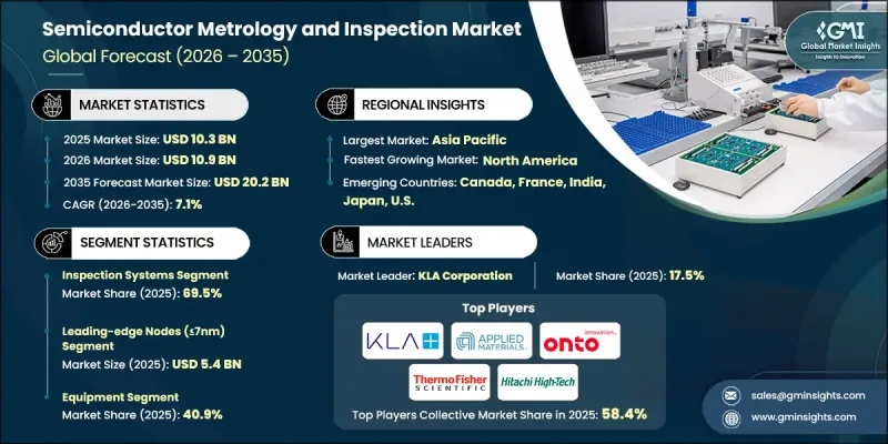
市場擴張的驅動力來自先進半導體節點日益複雜的發展、EUV和高數值孔徑微影術的應用,以及人工智慧和機器學習晶片需求的成長。向3D NAND和GAA架構的轉變也推動了對高精度測量和檢測解決方案的需求。先進的封裝和多層半導體結構需要高解析度、高可靠性的偵測系統來管理隨機缺陷並維持產量比率。此外,亞太地區代工廠產能的擴張以及混合測量解決方案在大批量生產設施中的普及也促進了市場成長。技術進步使得奈米級測量更加精確,從而改進了製程控制並最大限度地減少了缺陷造成的損失。這對於高效能運算和下一代半導體的生產至關重要。
| 市場範圍 | |
|---|---|
| 開始年份 | 2025 |
| 預測期 | 2026-2035 |
| 上市時的市場規模 | 103億美元 |
| 預測金額 | 202億美元 |
| 複合年成長率 | 7.1% |
EUV光刻技術的日益普及是半導體測量和檢測市場的主要驅動力。尤其是在7nm以下的製程節點,隨機缺陷和圖案偏差使得超高解析度偵測系統勢在必行。人工智慧/機器學習晶片需求的不斷成長,也要求更嚴格的製程控制,因為即使是奈米尺度的微小偏差也會對裝置效率和良率產生負面影響。先進封裝解決方案的產能擴張、製程節點向5nm以下的微型化以及對多層檢測日益成長的需求,都是推動市場成長的關鍵因素。在大批量晶圓廠中引入混合測量技術,能夠實現更快、更精確的測量,從而確保在複雜的製造環境中實現產量比率最佳化和製程一致性。
到2025年,檢測系統市佔率將達到69.5%。這些系統對於晶圓、遮罩和封裝層上的高精度缺陷檢測至關重要。檢測平台在提高產量比率、監控生產流程以及確保符合嚴格的先進節點製造標準方面發揮關鍵作用。它們使半導體製造商能夠有效地識別、分析和消除其整個量產生產線上的缺陷,因此對於希望在高性能晶片和人工智慧晶片生產領域保持競爭力的晶圓廠而言,這是一項必不可少的投資。
預計到2025年,7奈米以下(尖端節點)晶片市場規模將達54億美元,反映出市場對先進測量和檢測解決方案的旺盛需求。這些尖端節點需要極其精確的測量來支援極紫外光微影、多重圖形化技術以及GAA和FinFET架構。嚴格的缺陷接受度和複雜的製造流程使得先進的檢測和測量系統對於確保產量比率、裝置性能以及在高階運算應用中的競爭力至關重要。
到2025年,北美半導體測量和檢測市場佔有率將達到31.6%。這一區域成長主要得益於對本土半導體製造和製程精度的高度重視。人工智慧驅動的檢測系統、混合測量解決方案和製程線上監控技術的應用,為先進節點和大規模生產設施提供了有力支援。政府主導的措施、合作研究和產業夥伴關係正在加速關鍵尺寸測量、缺陷檢測和多層分析領域的創新。隨著北美晶圓廠優先考慮精度、產能最佳化和產量比率提升,該地區正逐步成為下一代測量和檢測技術的領導者。
目錄
第1章:調查方法和範圍
第2章執行摘要
第3章業界考察
- 生態系分析
- 供應商情況
- 利潤率
- 成本結構
- 每個階段增加的價值
- 影響價值鏈的因素
- 中斷
- 影響產業的因素
- 促進因素
- EUV微影術的複雜性要求檢測精度很高。
- 在小於 5nm 的節點上,對缺陷密度的敏感度會提高。
- 3D NAND 和 GAA 架構需要多層測量技術。
- 汽車晶片的製造標準要求零缺陷。
- 人工智慧/機器學習晶片需要更嚴格的製程控制公差。
- 產業潛在風險與挑戰
- 高昂的資本投資成本阻礙了中小企業採用該技術。
- 大規模生產製造中設備的吞吐量限制
- 市場機遇
- 異構和晶片封裝測試的成長
- 印度和東南亞新興的製造業正在尋求工具。
- 促進因素
- 成長潛力分析
- 監理情勢
- 北美洲
- 歐洲
- 亞太地區
- 拉丁美洲
- 中東和非洲
- 波特五力分析
- PESTEL 分析
- 科技與創新趨勢
- 當前技術趨勢
- 新興技術
- 價格趨勢
- 按地區
- 依產品
- 定價策略
- 新興經營模式
- 合規要求
- 專利和智慧財產權分析
第4章 競爭情勢
- 介紹
- 企業市佔率分析
- 按地區
- 北美洲
- 歐洲
- 亞太地區
- 拉丁美洲
- 中東和非洲
- 市場集中度分析
- 按地區
- 主要企業的競爭標竿分析
- 財務績效比較
- 銷售量
- 利潤率
- 研究與開發
- 產品系列比較
- 產品線寬度
- 科技
- 創新
- 區域擴張比較
- 全球擴張分析
- 服務網路覆蓋
- 按地區分類的市場滲透率
- 競爭定位矩陣
- 領導者
- 挑戰者
- 追蹤者
- 小眾玩家
- 戰略展望矩陣
- 財務績效比較
- 主要進展
- 併購
- 夥伴關係與合作
- 技術進步
- 擴張和投資策略
- 數位轉型計劃
- 新興競爭對手和Start-Ups競爭對手的發展趨勢
第5章 市場估算與預測:依設備類型分類,2022-2035年
- 測量系統
- 光學測量
- 電子束測量
- X光測量
- AFM 和其他
- 檢查系統
- 晶圓檢測
- 掩模/光罩測試
第6章 市場估計與預測:依衡量參數分類,2022-2035年
- 關鍵尺寸 (CD) 測量
- 疊加測量
- 薄膜厚度和材料測量
- 其他
第7章 市場估算與預測:依節點技術分類,2022-2035年
- 最先進節點(≤7nm)
- 先進節點(8-28nm)
- 成熟節點(28nm以上)
第8章 市場估算與預測:依產品類型分類,2022-2035年
- 裝置
- 軟體
- 服務
第9章 市場估計與預測:依應用領域分類,2022-2035年
- 晶圓製造
- 線上控制
- 離線控制
- 掩模/光罩製造
- 線上控制
- 離線控制
- 先進包裝
- 晶圓層次電子構裝(WLP)
- 3D IC
- 面板級包裝
第10章 市場估價與預測:依最終用戶分類,2022-2035年
- IDM
- 專業鑄造廠
- OSAT
第11章 市場估價與預測:按地區分類,2022-2035年
- 北美洲
- 美國
- 加拿大
- 歐洲
- 德國
- 英國
- 法國
- 西班牙
- 義大利
- 亞太地區
- 中國
- 印度
- 日本
- 澳洲
- 韓國
- 拉丁美洲
- 巴西
- 墨西哥
- 阿根廷
- 中東和非洲
- 南非
- 沙烏地阿拉伯
- 阿拉伯聯合大公國
第12章:公司簡介
- 主要企業
- Applied Materials, Inc.
- ASML Holding NV
- KLA Corporation
- Hitachi Ltd.
- Thermo Fisher Scientific Inc.
- 按地區分類的主要企業
- 北美洲
- Advantest Corporation
- Bruker Corporation
- Onto Innovation, Inc
- Nova Measuring Instruments Ltd.
- 亞太地區
- JEOL Ltd.
- Nikon Corporation
- Lasertec Corporation
- Toray Engineering Co., Ltd.
- Park Systems Corp.
- 歐洲
- Camtek Ltd.
- Olympus(EVIDENT)
- Zygo Corporation
- 北美洲
The Global Semiconductor Metrology and Inspection Market was valued at USD 10.3 billion in 2025 and is estimated to grow at a CAGR of 7.1% to reach USD 20.2 billion by 2035.
Market expansion is fueled by the increasing complexity of advanced semiconductor nodes, the adoption of EUV and High-NA lithography, and the rising demand for AI and machine learning chips. The shift toward 3D NAND and GAA architectures is also driving the need for precise metrology and inspection solutions. Advanced packaging and multi-layer semiconductor structures require high-resolution, reliable inspection systems to manage stochastic defects and maintain yield. Growth is further supported by increasing foundry capacities in APAC and the widespread adoption of hybrid metrology solutions in high-volume manufacturing facilities. Technological advancements are enabling more accurate nanoscale measurements, improving process control, and minimizing defect-related losses, which is critical for high-performance computing and next-generation semiconductor production.
| Market Scope | |
|---|---|
| Start Year | 2025 |
| Forecast Year | 2026-2035 |
| Start Value | $10.3 Billion |
| Forecast Value | $20.2 Billion |
| CAGR | 7.1% |
The increasing adoption of EUV lithography is a major driver of the semiconductor metrology and inspection market, particularly for sub-7nm nodes where stochastic defects and pattern variability demand ultra-high-resolution inspection systems. The growing requirement for AI/ML chips necessitates tighter process control, as even minor nanoscale variations can disrupt device efficiency and output. Rising production of advanced packaging solutions, scaling to sub-5nm nodes, and multi-layer inspection needs are key factors supporting market growth. The integration of hybrid metrology in high-volume fabs allows for faster, more accurate measurements, ensuring yield optimization and process consistency across complex manufacturing environments.
The inspection systems segment held a 69.5% share in 2025. These systems are crucial for detecting defects across wafers, masks, and packaging layers with high precision. Inspection platforms play a vital role in yield enhancement, process monitoring, and compliance with stringent advanced-node manufacturing standards. They allow semiconductor manufacturers to identify, analyze, and mitigate defects efficiently across high-volume production lines, making them an essential investment for fabs aiming to maintain competitiveness in high-performance and AI chip production.
The leading-edge nodes segment (<=7nm) held a market value of USD 5.4 billion in 2025, reflecting high demand for advanced metrology and inspection solutions. These cutting-edge nodes require extremely precise measurements to support EUV lithography, multi-patterning techniques, and GAA or FinFET architectures. Tight defect tolerances and complex production processes make advanced inspection and metrology systems indispensable for ensuring yield, device performance, and competitiveness in high-end computing applications.
North America Semiconductor Metrology and Inspection Market accounted for 31.6% share in 2025. Growth in this region is driven by a strong focus on domestic semiconductor manufacturing and process precision. The adoption of AI-driven inspection systems, hybrid metrology solutions, and in-line process monitoring supports advanced nodes and high-volume production facilities. Government initiatives, collaborative research, and industry partnerships are accelerating innovation in critical dimension measurement, defect detection, and multi-layer analysis. North American fabs emphasize precision, throughput optimization, and yield improvement, positioning the region as a leader in next-generation metrology and inspection technologies.
Key players operating in the Global Semiconductor Metrology and Inspection Market include Advantest Corporation, Applied Materials, Inc., ASML Holding N.V, Bruker Corporation, Camtek Ltd., Hitachi Ltd., JEOL Ltd., KLA Corporation, Lasertec Corporation, Nikon Corporation, Nova Measuring Instruments Ltd., Olympus (EVIDENT), Onto Innovation, Inc., Park Systems Corp., Thermo Fisher Scientific Inc., Toray Engineering Co., Ltd., and Zygo Corporation. Companies in the Semiconductor Metrology and Inspection Market are implementing strategies to strengthen market presence and expand global reach. They are investing in research and development to improve inspection resolution, metrology accuracy, and process integration for advanced nodes. Partnerships with semiconductor foundries, fabless companies, and equipment manufacturers enhance collaborative innovation and adoption of hybrid solutions. Firms are also focusing on expanding service portfolios, including in-line process control, predictive maintenance, and data analytics, to increase value for high-volume fabs. Geographic expansion, particularly in APAC and North America, ensures access to growing production facilities.
Table of Contents
Chapter 1 Methodology and Scope
- 1.1 Market scope and definition
- 1.2 Research design
- 1.2.1 Research approach
- 1.2.2 Data collection methods
- 1.3 Data mining sources
- 1.3.1 Global
- 1.3.2 Regional/Country
- 1.4 Base estimates and calculations
- 1.4.1 Base year calculation
- 1.4.2 Key trends for market estimation
- 1.5 Primary research and validation
- 1.5.1 Primary sources
- 1.6 Forecast model
- 1.7 Research assumptions and limitations
Chapter 2 Executive Summary
- 2.1 Industry 360° synopsis, 2022 - 2035
- 2.2 Key market trends
- 2.2.1 Equipment type trends
- 2.2.2 Measurement parameter trends
- 2.2.3 Node technology trends
- 2.2.4 Offering type trends
- 2.2.5 Application trends
- 2.2.6 End-user type trends
- 2.2.7 Regional trends
- 2.3 TAM Analysis, 2026-2035
- 2.4 CXO perspectives: Strategic imperatives
Chapter 3 Industry Insights
- 3.1 Industry ecosystem analysis
- 3.1.1 Supplier Landscape
- 3.1.2 Profit Margin
- 3.1.3 Cost structure
- 3.1.4 Value addition at each stage
- 3.1.5 Factor affecting the value chain
- 3.1.6 Disruptions
- 3.2 Industry impact forces
- 3.2.1 Growth drivers
- 3.2.1.1 EUV lithography complexity requires advanced inspection precision
- 3.2.1.2 Sub-5nm nodes increase defect density sensitivity
- 3.2.1.3 3D NAND and GAA architectures need multi-layer metrology
- 3.2.1.4 Automotive chips demand zero-defect manufacturing standards
- 3.2.1.5 AI/ML chips require tighter process control tolerances
- 3.2.2 Industry pitfalls and challenges
- 3.2.2.1 High capital cost limits SME adoption
- 3.2.2.2 Tool throughput constraints in high-volume fabs
- 3.2.3 Market opportunities
- 3.2.3.1 Growth in heterogeneous and chiplet packaging inspection
- 3.2.3.2 Emerging fabs in India and Southeast Asia demand tools
- 3.2.1 Growth drivers
- 3.3 Growth potential analysis
- 3.4 Regulatory landscape
- 3.4.1 North America
- 3.4.2 Europe
- 3.4.3 Asia Pacific
- 3.4.4 Latin America
- 3.4.5 Middle East & Africa
- 3.5 Porter's analysis
- 3.6 PESTEL analysis
- 3.7 Technology and Innovation landscape
- 3.7.1 Current technological trends
- 3.7.2 Emerging technologies
- 3.8 Price trends
- 3.8.1 By region
- 3.8.2 By product
- 3.9 Pricing Strategies
- 3.10 Emerging Business Models
- 3.11 Compliance Requirements
- 3.12 Patent and IP analysis
Chapter 4 Competitive Landscape, 2025
- 4.1 Introduction
- 4.2 Company market share analysis
- 4.2.1 By region
- 4.2.1.1 North America
- 4.2.1.2 Europe
- 4.2.1.3 Asia Pacific
- 4.2.1.4 Latin America
- 4.2.1.5 Middle East & Africa
- 4.2.2 Market concentration analysis
- 4.2.1 By region
- 4.3 Competitive benchmarking of key players
- 4.3.1 Financial performance comparison
- 4.3.1.1 Revenue
- 4.3.1.2 Profit margin
- 4.3.1.3 R&D
- 4.3.2 Product portfolio comparison
- 4.3.2.1 Product range breadth
- 4.3.2.2 Technology
- 4.3.2.3 Innovation
- 4.3.3 Geographic presence comparison
- 4.3.3.1 Global footprint analysis
- 4.3.3.2 Service network coverage
- 4.3.3.3 Market penetration by region
- 4.3.4 Competitive positioning matrix
- 4.3.4.1 Leaders
- 4.3.4.2 Challengers
- 4.3.4.3 Followers
- 4.3.4.4 Niche players
- 4.3.5 Strategic outlook matrix
- 4.3.1 Financial performance comparison
- 4.4 Key developments
- 4.4.1 Mergers and acquisitions
- 4.4.2 Partnerships and collaborations
- 4.4.3 Technological advancements
- 4.4.4 Expansion and investment strategies
- 4.4.5 Digital transformation initiatives
- 4.5 Emerging/ startup competitors landscape
Chapter 5 Market Estimates and Forecast, By Equipment Type, 2022 - 2035 (USD Million)
- 5.1 Key trends
- 5.2 Metrology systems
- 5.2.1 Optical metrology
- 5.2.2 E-beam metrology
- 5.2.3 X-ray metrology
- 5.2.4 AFM & others
- 5.3 Inspection systems
- 5.3.1 Wafer inspection
- 5.3.2 Mask/reticle inspection
Chapter 6 Market Estimates and Forecast, By Measurement Parameter, 2022 - 2035 (USD Million)
- 6.1 Key trends
- 6.2 Critical dimension (CD) metrology
- 6.3 Overlay metrology
- 6.4 Film thickness & material metrology
- 6.5 Others
Chapter 7 Market Estimates and Forecast, By Node Technology, 2022 - 2035 (USD Million)
- 7.1 Key trends
- 7.2 Leading-edge nodes (<=7nm)
- 7.3 Advanced nodes (8-28nm)
- 7.4 Mature nodes (>28nm)
Chapter 8 Market Estimates and Forecast, By Offering Type, 2022 - 2035 (USD Million)
- 8.1 Key trends
- 8.2 Equipment
- 8.3 Software
- 8.4 Services
Chapter 9 Market Estimates and Forecast, By Application, 2022 - 2035 (USD Million)
- 9.1 Key trends
- 9.2 Wafer fabrication
- 9.2.1 Inline control
- 9.2.2 Offline control
- 9.3 Mask/reticle fabrication
- 9.3.1 Inline control
- 9.3.2 Offline control
- 9.4 Advanced Packaging
- 9.4.1 Wafer-level packaging (WLP)
- 9.4.2 3D IC
- 9.4.3 Panel-level packaging
Chapter 10 Market Estimates and Forecast, By End-User Type, 2022 - 2035 (USD Million)
- 10.1 Key trends
- 10.2 IDMs
- 10.3 Pure-play foundries
- 10.4 OSATs
Chapter 11 Market Estimates and Forecast, By Region, 2022 - 2035 (USD Million)
- 11.1 Key trends
- 11.2 North America
- 11.2.1 U.S.
- 11.2.2 Canada
- 11.3 Europe
- 11.3.1 Germany
- 11.3.2 UK
- 11.3.3 France
- 11.3.4 Spain
- 11.3.5 Italy
- 11.4 Asia Pacific
- 11.4.1 China
- 11.4.2 India
- 11.4.3 Japan
- 11.4.4 Australia
- 11.4.5 South Korea
- 11.5 Latin America
- 11.5.1 Brazil
- 11.5.2 Mexico
- 11.5.3 Argentina
- 11.6 Middle East and Africa
- 11.6.1 South Africa
- 11.6.2 Saudi Arabia
- 11.6.3 UAE
Chapter 12 Company Profiles
- 12.1 Global Key Players
- 12.1.1 Applied Materials, Inc.
- 12.1.2 ASML Holding N.V
- 12.1.3 KLA Corporation
- 12.1.4 Hitachi Ltd.
- 12.1.5 Thermo Fisher Scientific Inc.
- 12.2 Regional key players
- 12.2.1 North America
- 12.2.1.1 Advantest Corporation
- 12.2.1.2 Bruker Corporation
- 12.2.1.3 Onto Innovation, Inc
- 12.2.1.4 Nova Measuring Instruments Ltd.
- 12.2.2 Asia Pacific
- 12.2.2.1 JEOL Ltd.
- 12.2.2.2 Nikon Corporation
- 12.2.2.3 Lasertec Corporation
- 12.2.2.4 Toray Engineering Co., Ltd.
- 12.2.2.5 Park Systems Corp.
- 12.2.3 Europe
- 12.2.3.1 Camtek Ltd.
- 12.2.3.2 Olympus (EVIDENT)
- 12.2.3.3 Zygo Corporation
- 12.2.1 North America
 全球半導體測量與測試市場:機會與策略展望(至2035年)
 半導體計量與測試市場分析及預測(至2035年):依類型、產品類型、服務、技術、組件、應用、裝置、製程及最終用戶分類
 半導體測量和測試設備市場:按測試類型、技術、晶圓廠類型、製程節點、國家和地區分類-全球產業分析、市場規模、市場佔有率和預測(2025-2032 年)
 半導體計量和檢測設備市場規模、佔有率、成長及全球產業分析:依類型、應用和地區劃分的洞察與預測(2026-2034)
 按技術、光罩類型、晶圓尺寸、應用和最終用途行業分類的光罩檢測和計量設備市場 - 全球預測 2026-2032半導體計量和檢測設備市場-2025-2030年預測
 模具分類設備:全球市佔率及排名、總收入及需求預測(2025-2031年)光罩檢測和計量設備 - 全球市場佔有率和排名、總收入和需求預測(2025-2031 年)
 半導體計量和檢測設備市場預測至2032年:按設備類型、技術、應用、最終用戶和地區分類的全球分析
 半導體計量和檢測設備市場規模、佔有率和趨勢分析報告:按技術、尺寸、製程節點、晶圓廠類型、地區和細分市場預測,2025 年至 2033 年