

 |
市場調查報告書
商品編碼
1721471
雷射光掩模市場機會、成長動力、產業趨勢分析及 2025 - 2034 年預測Laser Photomask Market Opportunity, Growth Drivers, Industry Trend Analysis, and Forecast 2025 - 2034 |
||||||
2024 年全球雷射光掩模市場價值為 48 億美元,預計到 2034 年將以 3% 的複合年成長率成長,達到 64 億美元。這一成長是由對先進半導體晶片組的需求不斷成長、電子元件的持續小型化以及消費性電子產品的激增所推動的。隨著半導體技術節點不斷縮小至3奈米以下水平,光刻製程的精確度變得更加重要。雷射光掩模對於這種轉變至關重要,它能夠將複雜的電路圖案精確地轉移到矽晶片上。這種對精確度的需求正在推動光掩模製造領域的重大創新和投資。
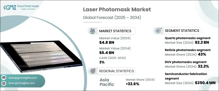
市場正在見證光掩模技術的重大進步,特別是針對日益複雜的半導體應用。隨著晶片製造商不斷突破製造界限,對高性能光掩模的需求也日益成長,到 2024 年,光罩光掩模市場的價值將達到 20 億美元。由於該領域在生產尖端光刻技術所需的高解析度圖案方面發揮著重要作用,因此其應用範圍正在不斷擴大。隨著極紫外線 (EUV) 和高 NA 光刻技術的興起,確保無缺陷掩模已成為重中之重,從而導致了能夠檢測奈米級缺陷的基於 AI 的檢測系統的整合。這不僅提高了生產良率,也提高了掩模修復精度。
| 市場範圍 | |
|---|---|
| 起始年份 | 2024 |
| 預測年份 | 2025-2034 |
| 起始值 | 48億美元 |
| 預測值 | 64億美元 |
| 複合年成長率 | 3% |
石英光掩模市場規模在 2024 年將達到 22 億美元,仍是市場的主要組成部分,預計到 2034 年複合年成長率將達到 3.2%。該材料卓越的熱性能和光學性能使其成為深紫外線 (DUV) 和 EUV 微影製程的理想選擇。最近的進展包括使用混合石英坯料結構來最大限度地減少光吸收不一致性,從而顯著提高光掩模的品質。這在人工智慧處理器、記憶體模組和其他高精度電子元件的生產中尤其重要,因為光罩的保真度直接影響設備效能。
預計美國雷射光掩模市場到 2024 年將創造 10 億美元的產值,到 2034 年的複合年成長率將達到 3.6%。這一成長主要得益於本地化半導體製造需求的不斷成長,以及政策激勵和技術進步的支持。對人工智慧運算的需求不斷成長,增加了對先進半導體節點的需求,進一步推動了光掩模的消費。隨著美國境內更多半導體工廠的建設,對最先進光掩模的需求預計將持續上升。
應用材料公司(Applied Materials Inc.)、Photronics Inc.、KLA Corporation 等領先公司處於市場前沿。為了保持競爭優勢,這些公司正在採用先進的自動化和人工智慧技術來簡化檢查流程、提高產量並最大限度地減少缺陷。他們還專注於開發與 EUV 相容的光掩模,並與半導體代工廠合作,為 3nm 以下節點量身定做掩模。擴大半導體中心的生產設施和增加下一代掩模材料的研發支出是滿足不斷成長的產業需求和確保市場領導地位的核心策略。
目錄
第1章:方法論與範圍
第2章:執行摘要
第3章:行業洞察
- 產業生態系統分析
- 供應商矩陣
- 利潤率分析
- 技術與創新格局
- 專利分析
- 重要新聞和舉措
- 產業衝擊力
- 成長動力
- 半導體晶片組需求不斷成長
- 電子元件快速小型化
- 消費性電子產品市場的擴張
- 提升品牌形象與市場差異化
- 增加半導體研發投入
- 產業陷阱與挑戰
- 高資本支出和生產成本
- 矽供應鏈的脆弱性
- 成長動力
- 成長潛力分析
- 波特的分析
- PESTEL分析
- 未來市場趨勢
- 監管格局
第4章:市場估計與預測:按光掩模類型,2021 年至 2034 年
- 主要趨勢
- 光罩
- 主光掩模
- 複製光掩模
第5章:市場估計與預測:依基板材料,2021 年至 2034 年
- 主要趨勢
- 石英光掩模
- 鈉鈣光掩模
- 薄膜光掩模
第6章:市場估計與預測:按技術,2021 年至 2034 年
- 主要趨勢
- EUV(極紫外線)光掩模
- DUV(深紫外線)光掩模
- 二元光掩模
- 相移光掩模
第7章:市場估計與預測:按應用,2021 年至 2034 年
- 主要趨勢
- 半導體製造
- 平面顯示器製造
- MEMS(微機電系統)
- IC封裝
- 光電子
- 其他
第8章:市場估計與預測:按最終用途產業,2021 年至 2034 年
- 主要趨勢
- 消費性電子產品
- 汽車
- 醫療保健和醫療器械
- 航太與國防
- 電信
- 其他
第9章:市場估計與預測:按地區,2021–2034
- 主要趨勢
- 北美洲
- 美國
- 加拿大
- 歐洲
- 德國
- 英國
- 法國
- 西班牙
- 義大利
- 歐洲其他地區
- 亞太地區
- 日本
- 中國
- 印度
- 韓國
- 澳新銀行
- 亞太其他地區
- 拉丁美洲
- 巴西
- 墨西哥
- 拉丁美洲其他地區
- 中東和非洲
- 南非
- 阿拉伯聯合大公國
- 沙烏地阿拉伯
- 中東和非洲其他地區
第10章:公司簡介
- Applied Materials Inc.
- KLA Corporation
- Photronics Inc.
- Toppan Photomasks, Inc.
- Dai Nippon Printing Co., Ltd. (DNP)
- Hoya Corporation
- LG Innotek Co., Ltd.
- SK-Electronics Co., Ltd.
- Compugraphics
- Nippon Filcon Co., Ltd.
- Lasertec Corporation
- Taiwan Mask Corporation (TMC)
- Qingyi Photomask Limited
- Hua Hong Semiconductor
- SUSS MicroTec SE
- Mycronic AB
- Carl Zeiss SMT GmbH
- Canon Inc.
- ASML Holding NV
- Nikon Corporation
- JEOL Ltd.
- Veeco Instruments Inc.
The Global Laser Photomask Market was valued at USD 4.8 billion in 2024 and is estimated to grow at a CAGR of 3% to reach USD 6.4 billion by 2034. This growth is being driven by the increasing demand for advanced semiconductor chipsets, the ongoing miniaturization of electronic components, and a surge in consumer electronics. As semiconductor technology nodes continue shrinking to sub-3nm levels, precision in lithographic processes has become more critical. Laser photomasks are crucial to this transformation, enabling the accurate transfer of complex circuit patterns onto silicon wafers. This need for precision is fueling significant innovation and investment in the photomask manufacturing sector.
The market is witnessing significant advancements in photomask technology, particularly in response to the growing complexity of semiconductor applications. As chipmakers push the boundaries of fabrication, there is an increasing demand for high-performance photomasks, with the reticle photomask segment valued at USD 2 billion in 2024. This segment is seeing greater adoption due to its essential role in producing the high-resolution patterns needed for cutting-edge lithography. With the rise of extreme ultraviolet (EUV) and high-NA lithography, ensuring defect-free masks has become a top priority, leading to the integration of AI-based inspection systems that can detect defects at the nanometer scale. This not only enhances production yield but also improves mask repair accuracy.
| Market Scope | |
|---|---|
| Start Year | 2024 |
| Forecast Year | 2025-2034 |
| Start Value | $4.8 Billion |
| Forecast Value | $6.4 Billion |
| CAGR | 3% |
Quartz photomasks, accounting for USD 2.2 billion in 2024, remain a dominant segment in the market, projected to grow at a CAGR of 3.2% through 2034. The material's exceptional thermal and optical properties make it ideal for deep ultraviolet (DUV) and EUV lithography processes. Recent advancements include the use of hybrid quartz-blank structures to minimize light absorption inconsistencies, significantly improving the quality of photomasks. This is especially important in the production of AI processors, memory modules, and other high-precision electronic components, where the fidelity of the mask directly affects device performance.
The United States Laser Photomask Market is estimated to generate USD 1 billion in 2024, growing at a CAGR of 3.6% through 2034. This growth is fueled by the rising demand for localized semiconductor manufacturing, supported by policy incentives and technological advances. The accelerating need for AI-powered computing has increased demand for advanced semiconductor nodes, further driving photomask consumption. With the construction of more semiconductor fabs within the U.S., the demand for state-of-the-art photomasks is expected to continue rising.
Leading companies such as Applied Materials Inc., Photronics Inc., and KLA Corporation are at the forefront of the market. To maintain a competitive edge, these companies are adopting advanced automation and AI technologies to streamline inspection processes, improve yield, and minimize defects. They are also focusing on developing EUV-compatible photomasks and collaborating with semiconductor foundries to create masks tailored for sub-3nm nodes. Expanding production facilities in semiconductor hubs and increasing R&D spending on next-gen mask materials are central strategies to meet growing industry demands and secure market leadership.
Table of Contents
Chapter 1 Methodology & Scope
- 1.1 Market scope & definitions
- 1.2 Research design
- 1.2.1 Research approach
- 1.2.2 Data collection methods
- 1.3 Base estimates & calculations
- 1.3.1 Base year calculation
- 1.3.2 Key trends for market estimation
- 1.4 Forecast model
- 1.5 Primary research and validation
- 1.5.1 Primary sources
- 1.5.2 Data mining sources
Chapter 2 Executive Summary
- 2.1 Industry 3600 synopsis
Chapter 3 Industry Insights
- 3.1 Industry ecosystem analysis
- 3.2 Vendor matrix
- 3.3 Profit margin analysis
- 3.4 Technology & innovation landscape
- 3.5 Patent analysis
- 3.6 Key news and initiatives
- 3.7 Industry impact forces
- 3.7.1 Growth drivers
- 3.7.1.1 Growing demand for semiconductor chipsets
- 3.7.1.2 Rapid miniaturization of electronic components
- 3.7.1.3 Expansion of the consumer electronics market
- 3.7.1.4 Enhanced Brand Image and Market Differentiation
- 3.7.1.5 Increased investment in semiconductor R&D
- 3.7.2 Industry pitfalls & challenges
- 3.7.2.1 High capital expenditure and production costs
- 3.7.2.2 Vulnerability to the silicon supply chain
- 3.7.1 Growth drivers
- 3.8 Growth potential analysis
- 3.9 Porter’s analysis
- 3.10 PESTEL analysis
- 3.11 Future market trends
- 3.12 Regulatory landscape
Chapter 4 Market Estimates and Forecast, By Photomask Type, 2021 – 2034 (USD Million & Million Units)
- 4.1 Key trends
- 4.2 Reticle photomasks
- 4.3 Master photomasks
- 4.4 Replicated photomasks
Chapter 5 Market Estimates and Forecast, By Substrate Material, 2021 – 2034 (USD Million & Million Units)
- 5.1 Key trends
- 5.2 Quartz photomasks
- 5.3 Soda-lime photomasks
- 5.4 Film photomasks
Chapter 6 Market Estimates and Forecast, By Technology, 2021 – 2034 (USD Million & Million Units)
- 6.1 Key trends
- 6.2 EUV (Extreme Ultraviolet) photomasks
- 6.3 DUV (Deep Ultraviolet) photomasks
- 6.4 Binary photomasks
- 6.5 Phase shift photomasks
Chapter 7 Market Estimates and Forecast, By Application, 2021 – 2034 (USD Million & Million Units)
- 7.1 Key trends
- 7.2 Semiconductor fabrication
- 7.3 Flat panel display manufacturing
- 7.4 MEMS (Micro-Electromechanical Systems)
- 7.5 IC packaging
- 7.6 Optoelectronics
- 7.7 Other
Chapter 8 Market Estimates and Forecast, By End Use Industry, 2021 – 2034 (USD Million & Million Units)
- 8.1 Key trends
- 8.2 Consumer electronics
- 8.3 Automotive
- 8.4 Healthcare & medical devices
- 8.5 Aerospace & defense
- 8.6 Telecommunication
- 8.7 Others
Chapter 9 Market Estimates and Forecast, By Region, 2021– 2034 (USD Million & Million Units)
- 9.1 Key trends
- 9.2 North America
- 9.2.1 U.S.
- 9.2.2 Canada
- 9.3 Europe
- 9.3.1 Germany
- 9.3.2 UK
- 9.3.3 France
- 9.3.4 Spain
- 9.3.5 Italy
- 9.3.6 Rest of Europe
- 9.4 Asia Pacific
- 9.4.1 Japan
- 9.4.2 China
- 9.4.3 India
- 9.4.4 South Korea
- 9.4.5 ANZ
- 9.4.6 Rest of Asia Pacific
- 9.5 Latin America
- 9.5.1 Brazil
- 9.5.2 Mexico
- 9.5.3 Rest of Latin America
- 9.6 Middle East and Africa
- 9.6.1 South Africa
- 9.6.2 UAE
- 9.6.3 Saudi Arabia
- 9.6.4 Rest of Middle East and Africa
Chapter 10 Company Profiles
- 10.1 Applied Materials Inc.
- 10.2 KLA Corporation
- 10.3 Photronics Inc.
- 10.4 Toppan Photomasks, Inc.
- 10.5 Dai Nippon Printing Co., Ltd. (DNP)
- 10.6 Hoya Corporation
- 10.7 LG Innotek Co., Ltd.
- 10.8 SK-Electronics Co., Ltd.
- 10.9 Compugraphics
- 10.10 Nippon Filcon Co., Ltd.
- 10.11 Lasertec Corporation
- 10.12 Taiwan Mask Corporation (TMC)
- 10.13 Qingyi Photomask Limited
- 10.14 Hua Hong Semiconductor
- 10.15 SUSS MicroTec SE
- 10.16 Mycronic AB
- 10.17 Carl Zeiss SMT GmbH
- 10.18 Canon Inc.
- 10.19 ASML Holding N.V.
- 10.20 Nikon Corporation
- 10.21 JEOL Ltd.
- 10.22 Veeco Instruments Inc.
 薄膜光掩模市場報告:趨勢、預測及競爭分析(至2035年)
 全球光掩模市場規模、佔有率、趨勢和成長分析報告(2026-2034)
 光掩模雷射修復系統市場:依產品類型、技術、最終用戶和應用分類-2026-2032年全球預測
 光掩模市場規模、佔有率、趨勢和預測:按產品類型、掩模加工類型、應用和地區分類(2026-2034 年)半導體掩模服務市場:依最終用戶、應用、製程節點、服務、掩模類型和晶圓尺寸分類,全球預測,2026-2032年
 全球先進光掩模技術市場:預測(至2034年)-按類型、材料、技術、應用、最終用戶和地區分類的分析
 2026年全球雷射光掩模市場報告全球晶片光掩模市場報告(2026 年)
 光掩模:市場佔有率分析、產業趨勢與統計、成長預測(2026-2031)光掩模清洗系統市場按產品類型、清洗技術、掩模類型和最終用戶分類 - 全球預測 2026-2032