


 |
市場調查報告書
商品編碼
2163332
先進包裝檢測系統:市場佔有率分析、產業趨勢與統計、成長預測(2026-2031)Advanced Packaging Inspection Systems - Market Share Analysis, Industry Trends & Statistics, Growth Forecasts (2026 - 2031) |
||||||

※ 本網頁內容可能與最新版本有所差異。詳細情況請與我們聯繫。
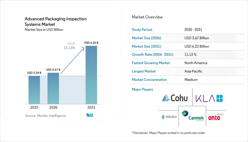
根據 Mordor Intelligence 預測,先進包裝偵測系統市場規模預計將在 2025 年達到 33.4 億美元,2026 年達到 36.7 億美元,到 2031 年達到 62.2 億美元,2026 年至 2031 年的複合年成長率為 11.13%。
全球先進包裝檢測系統市場趨勢及洞察
人工智慧和高效能運算正在推動異質融合。
由於人工智慧加速器封裝融合了多個晶片、高密度互連結構以及不同製程歷史的材料,因此是檢測難度最大的裝置之一。每個封裝晶圓在用於高價值系統之前,都必須經過檢測,包括進料基板品質、銅線路重布圖形化、微凸塊共面性、晶片佈局以及最終封裝完整性。 KLA 表示,預計其半導體製程控制產品組合中的先進封裝銷售額將從 2025 年的 6.35 億美元成長到 2026 年的 10 億美元。這項預測將製程控制支出與封裝產能的提升以及異質封裝中測量步驟的增加連結起來。隨著產能的提升,先進封裝檢測系統市場將受益,因為檢測需要在製造的多個階段進行,而不僅依賴最終檢測。此外,對於昂貴的多晶片封裝而言,每個成品更廣泛的檢測範圍降低了先進封裝檢測系統市場對晶片出貨量的依賴。
混合鍵結和細間距互連技術的廣泛應用
混合鍵結需要能夠同時處理極其精細的結構、嵌入式介面、表面狀況和生產吞吐量的檢測方法。根據電子元件失效分析協會 (ASM) 的研究,目前尚無任何單一方法能夠同時滿足所有混合鍵合製程所需的奈米級解析度、全區域覆蓋、亞表面可見性和生產吞吐量。因此,先進封裝檢測系統市場的製造商並未將混合鍵結檢測視為單一工具,而是在鍵合製程的每個階段採用不同的方法——光學、紅外線、聲學和 X光。 Onto Innovation 公司說明了一款線上混合鍵結工具,該工具結合了用於測量顆粒高度的 3D 測量技術和能夠識別介電層內空隙的紅外線檢測技術。 2026 年 7 月,Nova 公司宣布,一家全球領先的晶圓代工廠在經過競爭性評估後,選擇其 WMC 平台作為先進封裝測量的標準工具。這一趨勢正在推動先進封裝檢測系統市場的擴張,因為混合鍵合將單一的檢測點轉變為涉及多種物理測量要求的廣泛製程控制序列。
高資本投資與總擁有成本
當生產線上採用多種檢測技術時,先進封裝檢測系統需要大量的資本投入。此外,設備必須與無塵室的操作和維護流程整合。混合鍵結生產線可能需要光學、紅外線、聲學和X光系統等設備,每種系統都符合不同的物理測量要求。對於設備預算有限、財務能力不足以全面覆蓋線上檢測的半導體組裝和測試承包商而言,這種成本負擔尤其具有挑戰性。 2026年3月,Onto Innovation推出了Dragonfly G5,這是一款光學和照明系統,旨在支援單一平台上的多種HBM4相關應用。該平台設計體現了客戶對更廣泛功能的需求,無需為每個應用添加單獨的設備,同時保持先進封裝工作流程所需的靈敏度。如果難以資金籌措全面的線上檢測,小規模的先進封裝檢測系統市場參與企業可能會繼續採用抽樣檢測。然而,抽樣檢測可能會增加複雜多晶片產品的良率風險。
細分市場分析
2025年,光學檢測和測量系統佔據了先進封裝檢測系統市場42.51%的佔有率。這一領先地位反映了其高吞吐量、在晶圓級和組裝後流程中的廣泛應用,以及在晶圓廠和外包組裝廠的成熟部署。這些系統能夠測量多種封裝類型中線路重布的關鍵尺寸、進行凸塊共面性檢查、晶片偏移檢測和宏觀缺陷篩檢。在扇出型和覆晶生產中使用這些系統,符合大批量生產過程中對檢測速度和成本進行有效控制的需求。 2026年3月,Onto Innovation推出了先進封裝應用的Dragonfly G5,該產品具有150奈米缺陷靈敏度和多模照明功能。
紅外線和熱成像系統可偵測堆疊晶片結構內部的亞表面空隙和分層,而聲學系統則可識別表面光學無法偵測到的底部填充和封裝問題。電子束檢測可提供穿透矽通孔(TSV) 和後端互連的電學對比度圖像,SPIE 會議上的一篇論文報告稱,透過人工智慧驅動的計算採樣,缺陷晶片的檢測率提高了 4.3 倍。預計到 2031 年,X 光和電腦斷層掃描 (CT) 檢測系統將以 14.80% 的複合年成長率成長,成為該領域成長最快的技術。根據《微電子可靠性研究》期刊報導,高解析度奈米 CT 在 30 秒的概覽掃描中即可檢測到 20µm 微凸塊內的亞微米級空隙和裂縫。這項技術能夠檢測光學系統無法直接評估的嵌入式結、HBM 導電性和混合鍵結介面。
截至2025年,組裝後檢測將佔先進封裝檢測系統市場34.26%的佔有率。這一佔有率反映了自動化光學檢測(AOI)和3D檢測系統在切割後和封裝組裝過程中的應用。這些工具可在出貨前評估封裝的外觀、焊點相關特性、對準情況以及其他可透過視覺驗證的條件。對於所有封裝,包括採用成熟封裝製程製造的裝置,此類檢測仍然至關重要。此外,在處理多個客戶專案的大量生產的外包組裝業務中,也會用到此類檢測。
預計到2031年,先進封裝檢測系統中的晶圓級檢測市場將以14.29%的複合年成長率成長。這是因為在晶片貼裝前檢測缺陷可以防止成品多晶片封裝中的損耗。 2025年12月發表在《製造科學與工程雜誌》(Journal of Manufacturing Science and Engineering)上的一篇綜述指出,穿透矽通孔(TSV)、混合鍵結界面和微凸塊陣列正在推動對錶面和亞表面檢測需求的成長。 2025年8月,Nova公司發布了WMC,這是一款模組化光學測量平台,支援2.5D和3D整合、混合鍵結以及各種尺寸的晶圓。晶片級檢測可以防止已知有缺陷的晶片混入多晶片組件中,同時檢測結果會透過最終檢驗和失效分析回饋給上游製程團隊。 Cohu公司表示,其Neon平台將於2026年在其位於台灣的組裝基地進行HBM3、HBM4和HBM4E應用的認證測試。
區域分析
預計到2025年,亞太地區將佔據先進封裝檢測系統市場59.81%的佔有率。這一地位主要歸功於該地區在先進封裝能力、記憶體生產和半導體代工組裝業務方面的集中優勢。根據《台北時報》報道,工研院數據顯示,到2024年,台灣地區在全球IC封裝和測試生產中佔比將接近50%,韓國也開展重要的HBM封裝業務。日本則提供精密光學設備、電子束設備、半導體組裝代工製造及記憶體封裝生產能力。這些生產基地的存在使該地區在引進新設備和提供現場服務方面佔據了至關重要的地位。
中國在先進包裝檢測系統市場擁有大規模的傳統包裝基礎,對國產檢測設備的需求日益成長。根據Camtech的報告顯示,預計到2026年,中國市場將佔該公司銷售額的45%。隨著台灣以外地區代工組裝產能的擴張,馬來西亞、越南和新加坡的重要性日益凸顯。當現有工廠的前置作業時間延長時,這些國家的產能可以滿足部分需求。
預計到2031年,北美先進封裝檢測系統市場將以14.50%的複合年成長率成長,成為成長最快的地區。 SK海力士於2026年8月在印第安納州舉行了HBM封裝工廠的奠基儀式,該工廠預計將於2030年成為北美HBM生產基地。美國政府津貼支持封裝研究、中試生產能力、基板開發和材料研究。加拿大支持封裝研究,而墨西哥則在後端組裝和測試方面發揮作用。歐洲市場規模相對較小,主要由德國和荷蘭供應商主導,這些供應商主要服務X光、X光螢光和原子力顯微鏡應用。南美、中東和非洲市場規模仍然小規模,其需求與合約組裝和測試方面的投資密切相關。
其他好處:
- Excel格式的市場預測(ME)表
- 3個月的分析師支持
目錄
第1章:引言
- 研究假設和市場定義
- 調查範圍
第2章:調查方法
第3章執行摘要
第4章 市場狀況
- 市場概覽
- 市場促進因素
- 人工智慧和高效能運算正在推動異質融合。
- 混合鍵結和細間距互連技術的廣泛應用
- HBM 和 3D 記憶體堆疊技術的擴展
- 政府獎勵措施促進國內先進封裝產能
- 面板級封裝和玻璃芯基板生長
- 提高線上多模態檢測的盈利。
- 市場限制因素
- 初始投資和總擁有成本較高
- 先進包裝測量領域人員短缺
- 專用零件和供應鏈限制
- 互聯巡檢中的資料整合與網路安全風險
- 宏觀經濟因素對市場的影響
- 產業價值鏈分析
- 監理情勢
- 技術展望
- 光學和頻譜檢測
- 紅外線和地下檢測
- 2D、3D和X光電腦斷層掃描
- 人工智慧驅動的缺陷分類與預測過程控制
- 混合鍵結和晶片測試
- 現場檢查和線上檢查
- 面板級和玻璃基板檢測
- 波特五力分析
第5章 市場規模與成長預測
- 透過測試技術
- 光學檢測與測量系統
- 紅外線和熱成像檢測系統
- X光與電腦斷層掃描(CT)系統
- 電子束檢測系統
- 聲學和其他檢測系統
- 按測試階段
- 晶圓級檢測
- 晶片級和組件檢測
- 組裝後檢驗
- 最終檢驗和故障分析
- 透過包裝平台
- 2.5D中介層封裝
- 3D積體電路和HBM封裝
- 扇出包裝
- 風扇包裝
- 面板級包裝
- 系統套件
- 混合黏合包裝
- 嵌入式晶片和晶片封裝
- 按最終用戶行業分類
- 家用電子產品
- 資料中心和高效能運算
- 汽車/電動車
- 通訊與網路
- 醫療保健和醫療設備
- 航太/國防
- 研究和學術機構
- 其他終端用戶產業
- 按地區
- 北美洲
- 美國
- 加拿大
- 墨西哥
- 南美洲
- 巴西
- 阿根廷
- 其他南美國家
- 歐洲
- 德國
- 英國
- 法國
- 義大利
- 西班牙
- 其他歐洲國家
- 亞太地區
- 中國
- 日本
- 印度
- 韓國
- ASEAN
- 其他亞太國家
- 中東和非洲
- 中東
- 沙烏地阿拉伯
- 阿拉伯聯合大公國
- 土耳其
- 其他中東國家
- 非洲
- 南非
- 奈及利亞
- 其他非洲國家
- 中東
- 北美洲
第6章 競爭情勢
- 市場集中度
- 策略趨勢
- 市佔率分析
- 公司簡介
- KLA Corporation
- Onto Innovation Inc.
- Camtek Ltd.
- Cohu, Inc.
- Intekplus Co., Ltd.
- Semiconductor Technologies and Instruments Pte. Ltd.
- Lasertec Corporation
- Unity Semiconductor SAS
- Shenzhen Skyverse Technology Co., Ltd.
- Cheng Mei Instrument Technology Co., Ltd.
- Chroma ATE Inc.
- Toray Engineering Co., Ltd.
- TASMIT, Inc.
- Confovis GmbH
- Nova Ltd.
- Bruker Corporation
- Nearfield Instruments BV
- Comet Yxlon GmbH
- Hitachi High-Tech Corporation
- Tokyo Electron Limited
- JEOL Ltd.
第7章 市場機會與未來展望
According to Mordor Intelligence, the advanced packaging inspection systems market size was USD 3.34 billion in 2025, and USD 3.67 billion in 2026, and is projected to reach USD 6.22 billion by 2031, growing at a CAGR of 11.13% during 2026-2031.
Global Advanced Packaging Inspection Systems Market Trends and Insights
AI and High-Performance Computing Driving Heterogeneous Integration
AI accelerator packages are among the most difficult devices to inspect because they combine several dies, dense interconnect structures, and materials with different process histories. Every packaging wafer requires checks of incoming substrate quality, copper redistribution layer patterning, micro-bump coplanarity, die placement, and final package integrity before it can support a high-value system. KLA stated that advanced packaging revenue in its semiconductor process control portfolio was expected to rise from USD 635 million in 2025 to USD 1 billion in 2026. This company result links process-control spending to added packaging capacity and to the larger number of measurement steps used on heterogeneous packages. The advanced packaging inspection systems market benefits when capacity additions require inspection at multiple manufacturing stages rather than relying on a final check alone. Tool demand in the advanced packaging inspection systems market also becomes less dependent on chip volumes because costly multi-die packages require greater inspection coverage for each finished unit.
Rising Hybrid Bonding and Fine-Pitch Interconnect Adoption
Hybrid bonding requires inspection methods that can address very small features, buried interfaces, surface conditions, and production throughput at the same time. An ASM Electronic Device Failure Analysis Society study found that no single method provides nanoscale resolution, full-field coverage, subsurface visibility, and manufacturing-compatible throughput across all hybrid-bonding stages. Manufacturers in the advanced packaging inspection systems market, therefore, use optical, infrared, acoustic, and X-ray approaches at distinct points in the bonding flow, rather than treating hybrid-bond inspection as one tool purchase. Onto Innovation described in-line hybrid-bonding tools that combine 3D metrology for particle-height measurement with infrared inspection that can identify voids in dielectric layers. Nova announced in July 2026 that a leading global foundry had selected its WMC platform as its tool of record for advanced packaging measurements following a competitive evaluation. This shift expands the advanced packaging inspection systems market because hybrid bonding transforms a single inspection point into a broader process-control sequence with multiple physical measurement requirements.
High Capital and Total Cost of Ownership
Advanced packaging inspection systems require significant capital outlay when a production line uses several inspection technologies, and the equipment must also be integrated with cleanroom operations and maintenance practices. A hybrid-bonding line may need optical, infrared, acoustic, and X-ray tools, with each system serving a different physical measurement requirement. That cost burden is especially difficult for outsourced semiconductor assembly and test providers with narrower equipment budgets and less room to fund full inline coverage. Onto Innovation launched Dragonfly G5 in March 2026 with an optics and illumination design intended to support several HBM4-related applications on one platform. The platform's design reflects customer demand for broader capability without adding a separate tool for every application, while preserving the sensitivity needed for advanced package workflows. Smaller participants in the advanced packaging inspection systems market may continue to use sampling where comprehensive inline inspection is difficult to fund, even though sampling can leave more yield risk in complex multi-die products.
Other drivers and restraints analyzed in the detailed report include:
- Expansion of HBM and 3D Memory Stacking
- Government Incentives for Domestic Advanced Packaging Capacity
- Shortage of Advanced Packaging Metrology Talent
For complete list of drivers and restraints, kindly check the Table Of Contents.
Segment Analysis
Optical-based inspection and metrology systems held 42.51% of the advanced packaging inspection systems market share in 2025. Their leading position reflects high throughput, broad use across wafer-level and post-assembly flows, and an established installed base at wafer fabs and outsourced assembly sites. These systems support redistribution layer critical-dimension measurement, bump coplanarity checks, die-shift detection, and macro-defect screening across several package types. Their use in fan-out and flip-chip production aligns with the need to manage inspection speed and cost in high-volume flows. Onto Innovation launched Dragonfly G5 in March 2026 with stated 150 nm defect sensitivity and multi-mode illumination for advanced packaging applications.
Infrared and thermal systems find subsurface voids and delamination in stacked-die structures, while acoustic systems identify underfill and encapsulant issues beyond the reach of surface optical methods. Electron-beam inspection provides electrical-contrast imaging for through-silicon vias and back-end interconnects, and an SPIE paper reported defective-die capture rates up to 4.3 times higher through AI-guided computational sampling. X-ray and computed tomography inspection systems are projected to grow at a 14.80% CAGR through 2031, the highest rate in this segmentation. Research in Microelectronics Reliability showed that high-resolution nano-CT detected sub-micron voids and cracks in 20 µm micro-bumps during a 30-second overview scan. This capability supports inspection of buried joints, HBM continuity, and hybrid-bond interfaces that optical systems cannot directly assess.
Post-assembly inspection held 34.26% of the share in the advanced packaging inspection systems sector in 2025. Its position reflects the installed base of automated optical inspection and 3D inspection systems used after dicing and during package assembly. These tools assess package appearance, solder-related features, alignment, and other visible conditions before shipment. The category remains necessary for every package, including devices made through mature packaging methods. It also serves outsourced assembly operations that process high volumes across multiple customer programs.
Wafer-level inspection in the advanced packaging inspection systems market is projected to expand at a 14.29% CAGR through 2031 because defects found before die attach can prevent loss in a completed multi-die package. A December 2025 review in the Journal of Manufacturing Science and Engineering found that through-silicon vias, hybrid bonding interfaces, and micro-bump arrays are raising requirements for surface and subsurface inspection. Nova released the WMC in August 2025 as a modular optical metrology platform for 2.5D and 3D integration, hybrid bonding, and different wafer sizes. Die-level inspection prevents known-defective dies from entering multi-die assemblies, while final inspection and failure analysis feed findings back to upstream process teams. Cohu stated that its Neon platform was being qualified at a Taiwan-based outsourced assembly site for HBM3, HBM4, and HBM4E applications in 2026.
Complete Report Scope:
- By Inspection Technology
- Optical-Based Inspection and Metrology Systems
- Infrared and Thermal Inspection Systems
- X-Ray and Computed Tomography Inspection Systems
- Electron-Beam Inspection Systems
- Acoustic and Other Inspection Systems
- By Inspection Stage
- Wafer-Level Inspection
- Die-Level and Component Inspection
- Post-Assembly Inspection
- Final Inspection and Failure Analysis
- By Packaging Platform
- 2.5D Interposer Packaging
- 3D Integrated Circuit and HBM Packaging
- Fan-Out Packaging
- Fan-In Packaging
- Panel-Level Packaging
- System-in-Package
- Hybrid-Bonded Packaging
- Embedded-Die and Chiplet Packaging
- By End-User Industries
- Consumer Electronics
- Data Centers and High-Performance Computing
- Automotive and Electric Vehicles
- Telecommunications and Networking
- Healthcare and Medical Devices
- Aerospace and Defense
- Research and Academic Institutions
- Other End-User Industries
- By Geography
- North America
- United States
- Canada
- Mexico
- South America
- Brazil
- Argentina
- Rest of South America
- Europe
- Germany
- United Kingdom
- France
- Italy
- Spain
- Rest of Europe
- Asia-Pacific
- China
- Japan
- India
- South Korea
- ASEAN
- Rest of Asia-Pacific
- Middle East and Africa
- Middle East
- Saudi Arabia
- United Arab Emirates
- Turkey
- Rest of the Middle East
- Africa
- South Africa
- Nigeria
- Rest of Africa
- Middle East
- North America
Geography Analysis
Asia-Pacific held 59.81% of the share in the advanced packaging inspection systems sector in 2025. Its position follows the region's concentration of advanced packaging capacity, memory production, and outsourced semiconductor assembly operations. Taiwan accounted for nearly 50% of global IC packaging and testing output in 2024, based on ITRI data reported by the Taipei Times, and South Korea adds major HBM packaging activity. Japan contributes precision optics, electron-beam suppliers, outsourced assembly operations, and memory packaging capacity. These production centers make the region important for new equipment installations and field service.
China has a large legacy packaging base within the advanced packaging inspection systems market and an increasing interest in domestically sourced inspection equipment. Camtek reported that China represented 45% of its 2026 revenue. Malaysia, Vietnam, and Singapore are gaining relevance as outsourced assembly capacity expands beyond Taiwan. Their capacity can absorb part of the demand when lead times at established facilities lengthen.
North America in the advanced packaging inspection systems market is projected to grow at a 14.50% CAGR through 2031, making it the fastest-growing geography. SK Hynix held a groundbreaking ceremony in August 2026 for an HBM packaging facility in Indiana that was expected to be a North American HBM production base by 2030. U.S. public awards support packaging research, pilot capacity, substrate development, and materials work. Canada supports packaging research, and Mexico has a role in back-end assembly and test. Europe has a more modest position, led by German and Dutch suppliers serving X-ray, X-ray fluorescence, and atomic-force-metrology applications. South America and the Middle East and Africa remain smaller markets where demand follows contract assembly and test investment.
- KLA Corporation
- Onto Innovation Inc.
- Camtek Ltd.
- Cohu, Inc.
- Intekplus Co., Ltd.
- Semiconductor Technologies and Instruments Pte. Ltd.
- Lasertec Corporation
- Unity Semiconductor SAS
- Shenzhen Skyverse Technology Co., Ltd.
- Cheng Mei Instrument Technology Co., Ltd.
- Chroma ATE Inc.
- Toray Engineering Co., Ltd.
- TASMIT, Inc.
- Confovis GmbH
- Nova Ltd.
- Bruker Corporation
- Nearfield Instruments B.V.
- Comet Yxlon GmbH
- Hitachi High-Tech Corporation
- Tokyo Electron Limited
- JEOL Ltd.
Additional Benefits:
- The market estimate (ME) sheet in Excel format
- 3 months of analyst support
TABLE OF CONTENTS
1 INTRODUCTION
- 1.1 Study Assumptions and Market Definition
- 1.2 Scope of the Study
2 RESEARCH METHODOLOGY
3 EXECUTIVE SUMMARY
4 MARKET LANDSCAPE
- 4.1 Market Overview
- 4.2 Market Drivers
- 4.2.1 AI and High-Performance Computing Driving Heterogeneous Integration
- 4.2.2 Rising Hybrid Bonding and Fine-Pitch Interconnect Adoption
- 4.2.3 Expansion of HBM and 3D Memory Stacking
- 4.2.4 Government Incentives for Domestic Advanced Packaging Capacity
- 4.2.5 Growth of Panel-Level Packaging and Glass-Core Substrates
- 4.2.6 Increasing Yield Economics of Inline Multimodal Inspection
- 4.3 Market Restraints
- 4.3.1 High Capital and Total Cost of Ownership
- 4.3.2 Shortage of Advanced Packaging Metrology Talent
- 4.3.3 Specialty Component and Supply-Chain Constraints
- 4.3.4 Data-Integration and Cybersecurity Risk in Connected Inspection
- 4.4 Impact of Macroeconomic Factors on the Market
- 4.5 Industry Value-Chain Analysis
- 4.6 Regulatory Landscape
- 4.7 Technological Outlook
- 4.7.1 Optical and Multispectral Inspection
- 4.7.2 Infrared and Subsurface Inspection
- 4.7.3 2D, 3D, and X-Ray Computed Tomography
- 4.7.4 AI-Based Defect Classification and Predictive Process Control
- 4.7.5 Hybrid Bonding and Chiplet Inspection
- 4.7.6 In-Situ and Inline Inspection
- 4.7.7 Panel-Level and Glass-Substrate Inspection
- 4.8 Porter's Five Forces Analysis
- 4.8.1 Bargaining Power of Suppliers
- 4.8.2 Bargaining Power of Buyers
- 4.8.3 Threat of New Entrants
- 4.8.4 Threat of Substitutes
- 4.8.5 Intensity of Competitive Rivalry
5 MARKET SIZE AND GROWTH FORECASTS (VALUE)
- 5.1 By Inspection Technology
- 5.1.1 Optical-Based Inspection and Metrology Systems
- 5.1.2 Infrared and Thermal Inspection Systems
- 5.1.3 X-Ray and Computed Tomography Inspection Systems
- 5.1.4 Electron-Beam Inspection Systems
- 5.1.5 Acoustic and Other Inspection Systems
- 5.2 By Inspection Stage
- 5.2.1 Wafer-Level Inspection
- 5.2.2 Die-Level and Component Inspection
- 5.2.3 Post-Assembly Inspection
- 5.2.4 Final Inspection and Failure Analysis
- 5.3 By Packaging Platform
- 5.3.1 2.5D Interposer Packaging
- 5.3.2 3D Integrated Circuit and HBM Packaging
- 5.3.3 Fan-Out Packaging
- 5.3.4 Fan-In Packaging
- 5.3.5 Panel-Level Packaging
- 5.3.6 System-in-Package
- 5.3.7 Hybrid-Bonded Packaging
- 5.3.8 Embedded-Die and Chiplet Packaging
- 5.4 By End-User Industries
- 5.4.1 Consumer Electronics
- 5.4.2 Data Centers and High-Performance Computing
- 5.4.3 Automotive and Electric Vehicles
- 5.4.4 Telecommunications and Networking
- 5.4.5 Healthcare and Medical Devices
- 5.4.6 Aerospace and Defense
- 5.4.7 Research and Academic Institutions
- 5.4.8 Other End-User Industries
- 5.5 By Geography
- 5.5.1 North America
- 5.5.1.1 United States
- 5.5.1.2 Canada
- 5.5.1.3 Mexico
- 5.5.2 South America
- 5.5.2.1 Brazil
- 5.5.2.2 Argentina
- 5.5.2.3 Rest of South America
- 5.5.3 Europe
- 5.5.3.1 Germany
- 5.5.3.2 United Kingdom
- 5.5.3.3 France
- 5.5.3.4 Italy
- 5.5.3.5 Spain
- 5.5.3.6 Rest of Europe
- 5.5.4 Asia-Pacific
- 5.5.4.1 China
- 5.5.4.2 Japan
- 5.5.4.3 India
- 5.5.4.4 South Korea
- 5.5.4.5 ASEAN
- 5.5.4.6 Rest of Asia-Pacific
- 5.5.5 Middle East and Africa
- 5.5.5.1 Middle East
- 5.5.5.1.1 Saudi Arabia
- 5.5.5.1.2 United Arab Emirates
- 5.5.5.1.3 Turkey
- 5.5.5.1.4 Rest of the Middle East
- 5.5.5.2 Africa
- 5.5.5.2.1 South Africa
- 5.5.5.2.2 Nigeria
- 5.5.5.2.3 Rest of Africa
- 5.5.5.1 Middle East
- 5.5.1 North America
6 COMPETITIVE LANDSCAPE
- 6.1 Market Concentration
- 6.2 Strategic Moves
- 6.3 Market Share Analysis
- 6.4 Company Profiles (includes Global Level Overview, Market Level Overview, Core Segments, Financials as available, Strategic Information, Market Rank/Share, Products and Services, Recent Developments)
- 6.4.1 KLA Corporation
- 6.4.2 Onto Innovation Inc.
- 6.4.3 Camtek Ltd.
- 6.4.4 Cohu, Inc.
- 6.4.5 Intekplus Co., Ltd.
- 6.4.6 Semiconductor Technologies and Instruments Pte. Ltd.
- 6.4.7 Lasertec Corporation
- 6.4.8 Unity Semiconductor SAS
- 6.4.9 Shenzhen Skyverse Technology Co., Ltd.
- 6.4.10 Cheng Mei Instrument Technology Co., Ltd.
- 6.4.11 Chroma ATE Inc.
- 6.4.12 Toray Engineering Co., Ltd.
- 6.4.13 TASMIT, Inc.
- 6.4.14 Confovis GmbH
- 6.4.15 Nova Ltd.
- 6.4.16 Bruker Corporation
- 6.4.17 Nearfield Instruments B.V.
- 6.4.18 Comet Yxlon GmbH
- 6.4.19 Hitachi High-Tech Corporation
- 6.4.20 Tokyo Electron Limited
- 6.4.21 JEOL Ltd.
7 MARKET OPPORTUNITIES AND FUTURE OUTLOOK
- 7.1 White-Space and Unmet-Need Assessment

 包裝測試市場:依產品類型、材料、技術、終端用戶產業及地區分類
 先進包裝檢測與測量設備:全球市佔率及排名、總收入及需求預測(2026-2032年)
 包裝測試市場:依測試類型、包裝類型、最終用途產業和供應商類型分類-2026-2032年全球預測包裝實體性能測試設備市場(按設備類型、材料、技術、最終用戶和銷售管道),全球預測(2026-2032年)按封裝形式、測試服務、材料、終端用戶產業和保護技術分類的元件封裝和測試市場,全球預測,2026-2032年
 全球包裝測試市場規模、佔有率、趨勢和成長分析報告(2026-2034年)
 先進包裝檢測系統:全球市場佔有率和排名、總收入和需求預測(2025-2031 年)包裝測試機:全球市佔率排名、總銷售額和需求預測(2025-2031年)
 包裝測試市場機會、成長動力、產業趨勢分析和 2024 年至 2032 年預測