


 |
市場調查報告書
商品編碼
2123403
薄膜封裝:市場佔有率分析、產業趨勢與統計資料、成長預測(2026-2031)Thin Film Encapsulation - Market Share Analysis, Industry Trends & Statistics, Growth Forecasts (2026 - 2031) |
||||||

※ 本網頁內容可能與最新版本有所差異。詳細情況請與我們聯繫。
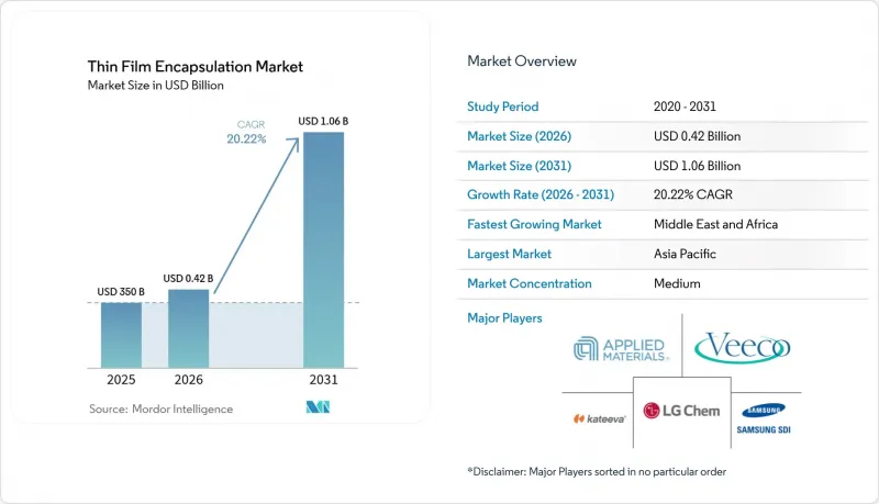
據 Mordor Intelligence 稱,薄膜封裝市場預計到 2026 年價值 4.2077 億美元,高於 2025 年的 3.5 億美元,預計到 2031 年將達到 10.6 億美元。
預計 2026 年至 2031 年的複合年成長率為 20.22%。
本報告按技術(例如,等離子體增強化學氣相沉積、原子層沉積)、層級構造(例如,無機多層阻擋層、有機多層阻擋層)、應用(例如,軟性OLED顯示器)、沉積設備類型(例如,叢集PECVD系統)、終端用戶產業(例如,家用電子電器、可再生能源)和地區進行分類。
全球薄膜封裝市場趨勢與洞察
韓國和中國 AMOLED 產能的擴張帶動了 ALD-TFE 設備的訂單。
三星顯示器公司正投資30億美元建造第8.6代IT OLED生產線,目標是2026年投產;京東方也投資87億美元興建類似工廠。這些項目帶動了ALD封裝設備訂單的激增,因為這項技術能夠提供低溫、均勻且無針孔的隔離層,而這對於下一代IT和汽車面板至關重要。日益激烈的競爭使韓國製造商重新奪回了出貨量的主導,同時亞太地區各代工廠對ALD的需求也在不斷成長。
歐盟和北美強制使用曲面汽車顯示螢幕
監管指南推薦採用無縫儀錶叢集,這加速了曲面OLED儀錶板設計的普及。這些模組需要一種能夠承受振動、紫外線輻射和低至-40 度C溫度循環的封裝層。三星採用先進防潮層的串聯OLED面板,正是這一轉變的標誌。預計到2026年,汽車顯示器總支出將超過顯示器面板銷售額,三星可望從中獲利。
第六代ALD叢集線的高資本投入
引進新一代ALD堆疊技術需要每條生產線超過1億美元的投資,阻礙了中型製造商進入市場,並減緩了技術的普及應用。許多亞洲製造工廠仍在攤銷過時的叢集設備,即使良率提升顯而易見,升級改造的經濟效益也難以承受。這種成本壁壘阻礙了薄膜封裝市場全面採用一流的封裝技術。
細分市場分析
預計到2025年,原子層沉積(ALD)的複合年成長率將達到25.85%,而等離子體增強化學氣相沉積(PECVD)的銷售額將佔38.90%,這凸顯了薄膜封裝市場正處於轉型期。 ALD薄膜的水蒸氣透過率已達到10⁻⁶ g/m²/天,延長了OLED的使用壽命,並使其能夠使用折疊式基板。卷對卷(R2R)ALD正在提高生產效率,使其達到適用於穿戴式產品生產的捲材速度,而空間ALD則正在克服基板尺寸的限制。對於需要大規模生產的剛性面板,PECVD仍然是首選。 VTE和OVPD繼續應用於一些小眾的發光堆疊領域,在這些領域,材料相容性比極致的隔離層性能更為重要。低溫ALD化學技術已於2023年獲得SID的獎勵,它使得聚醯亞胺基板能夠實用化大規模生產的折疊式裝置,進一步豐富了此技術的應用範圍。因此,ALD 設備製造商的訂單訂單創歷史新高,重振了韓國、中國和美國的區域供應商生態系統。
在薄膜封裝市場,對成本敏感的產品仍然依賴PECVD製程。這是因為PECVD反應器可以與現有的TFT生產線無縫整合。 Kateeva的噴墨封裝印刷技術減少了有機廢棄物,並實現了智慧型手錶的圖案化隔離層。在小面積微顯示器領域,裝置良率比產量更為重要,因此VTE製程仍然至關重要。在前導測試中,空間ALD製程成功處理了第15代基板,預計PECVD和ALD之間的競爭將進一步加劇,加速採用結合兩種製程的混合生產線。
結合聚對二甲苯C和ALD氧化鋁的混合層壓結構在應力鬆弛和防潮性能之間實現了平衡,預計到2025年將佔市場佔有率的46.85%。此組合材料的透濕率低於105 g/m²/天,同時保持超過10,000次的彎曲循環,滿足高階智慧型手機的規格要求。同時,單層阻隔材料目前以28.35%的複合年成長率佔據市場主導地位。這是因為含銀離子的混合薄膜在提供同等防護性能的同時,將沉積製程時間縮短了一半,從而縮短了捲材面板的生產週期。
無機多層結構具有無與倫比的抗氧性能,但在拉伸應力下容易開裂,限制了其在折疊式設備中的應用。有機多層結構具有很高的柔韌性,但其本身很少能達到預期的使用壽命。因此,在批量生產線上,層級構造需要根據不同產品類型進行客製化。智慧型手機採用混合層級構造,汽車叢集需要三層無機蓋罩層,而電子紡織品則越來越依賴先進的有機化學技術。為了解決這個問題,組件供應商提供模組化材料套件,以協調相鄰層之間的屈光、模量和黏合力,從而確保生產線的可靠性,良率超過90%。
區域分析
亞太地區在韓國和中國晶圓廠及一體化供應鏈生態系統的推動下,預計2025年將維持69.10%的市場佔有率。政府為補貼封裝資本投資成本而獎勵加速了原子層沉積(ALD)叢集的普及,而韓國企業則將業務重心轉向高附加價值產品和疊層結構,以保障利潤率。區域設備和化學品供應商紛紛在晶圓廠附近設立分支機構,縮短了認證週期,並鞏固了其在薄膜封裝市場的主導地位。
在歐洲,受汽車和建築光伏發電(BIPV)需求的推動,市場呈現強勁成長。歐盟嚴格的汽車安全指令加速了曲面OLED駕駛座的普及,而碳中和建築法規則促進了ALD隔離層在太陽能帷幕牆的應用。該研究聯盟致力於開發低溫ALD前驅體,使其性能符合循環經濟目標。
儘管中東和非洲地區的基數小規模,但預計其複合年成長率將高達26.35%,這主要得益於阿拉伯聯合大公國和沙烏地阿拉伯等國為實現經濟多元化而對電子產業叢集的投入。嚴酷的沙漠氣候使得堅固封裝技術對顯示器和太陽能電池產品至關重要,從而催生了對基於原子層沉積(ALD)的無機薄膜的高階需求。與亞洲原始設備製造商(OEM)的技術轉移夥伴關係,已幫助該地區建立了本地生產能力,並降低了全球品牌對單一地區的依賴。
儘管面板生產規模有限,北美憑藉其在材料科學和設備出口方面的領先地位,依然保持著影響力。汽車產業的法規以及量子點和微型LED的研發推動了對專用阻隔技術的需求,而卷對卷原子層沉積(ALD)新創公司則利用創業投資資金實現了穿戴式產品線的商業化。區域晶圓廠與大學合作,利用機器學習技術進行製程控制,以提高薄膜的均勻性和生產效率。
其他好處:
- Excel格式的市場預測(ME)表
- 3個月的分析師支持
目錄
第1章:引言
- 研究假設和市場定義
- 調查範圍
第2章:調查方法
第3章執行摘要
第4章 市場狀況
- 市場概覽
- 市場促進因素
- 韓國和中國 AMOLED 產能的擴張帶動了 ALD-TFE 設備的訂單。
- 歐盟和北美強制使用曲面汽車顯示螢幕
- 卷對卷ALD技術能夠實現經認證的醫療穿戴式裝置。
- 歐盟推動光伏建築整合(BIPV)實現碳中和,增加了無機材料的應用門檻。
- 低溫ALD材料可用於製造折疊式設備,榮獲SID獎。
- 中國的「新型顯示器」補貼旨在鼓勵對封裝設備的投資。
- 市場限制因素
- 第六代ALD叢集線的高資本投入
- 汽車循環測試中在低於-40 度C。
- 來自超薄軟性玻璃的競爭
- 前驅物供應瓶頸(例如,DEZ)
- 價值鏈分析
- 監管和技術展望
- 關鍵績效指標基準
- 波特五力模型
- 評估宏觀經濟因素對市場的影響
第5章 市場規模與成長預測
- 透過技術
- 等離子體增強化學氣相沉積(PECVD)
- 原子層沉積(ALD)
- 噴墨列印
- 真空熱沉澱(VTE)
- 有機氣相外延(OVPD)
- 卷對卷ALD
- 其他新興技術(聚對二甲苯、溶膠-凝膠法)
- 按層級構造
- 無機多層隔離層
- 有機多層屏障
- 混合(有機+無機)屏障
- 封裝
- 透過使用
- 軟性OLED顯示螢幕
- 薄膜太陽能電池
- 軟性OLED照明
- 穿戴式和醫療用電子設備
- 汽車顯示器和照明
- 量子點和微型LED元件
- 印刷感測器和物聯網設備
- 薄膜沉積設備類型
- 叢集PECVD系統
- 噴墨封裝印表機
- ALD反應器
- 卷對卷真空系統
- 雷射輔助薄膜沉積系統
- 按最終用途行業分類
- 家用電子產品
- 可再生能源
- 汽車和運輸業
- 醫療保健和穿戴式設備
- 工業和航太
- 按地區
- 北美洲
- 美國
- 加拿大
- 墨西哥
- 南美洲
- 巴西
- 阿根廷
- 其他南美國家
- 歐洲
- 德國
- 法國
- 英國
- 義大利
- 其他歐洲國家
- 亞太地區
- 中國
- 韓國
- 日本
- 印度
- 其他亞太國家
- 中東和非洲
- 中東
- 沙烏地阿拉伯
- 阿拉伯聯合大公國
- 土耳其
- 其他中東國家
- 非洲
- 南非
- 奈及利亞
- 其他非洲國家
- 中東
- 北美洲
第6章 競爭情勢
- 市場集中度
- 策略趨勢
- 市佔率分析
- 公司簡介
- Samsung SDI Co., Ltd.
- LG Chem Ltd.
- Universal Display Corporation
- Applied Materials Inc.
- Veeco Instruments Inc.
- 3M Inc.
- Toray Industries Inc.
- Kateeva
- BASF(Rolic)AG
- Meyer Burger Technology AG
- Encapsulix SAS
- Forge Nano Inc.
- Aixtron SE
- Angstrom Engineering Inc.
- Forge Nano Inc.
- Beneq Oy
- Picosun Oy
- Canon Tokki Corporation
- AP Systems
- EMD Electronics(Merck KGaA)
- Idemitsu Kosan Co.
- Encapsulix SAS
- Wonik IPS
- Vitriflex Inc.
第7章 市場機會與未來展望
According to Mordor Intelligence, thin film encapsulation market size in 2026 is estimated at USD 420.77 million, growing from 2025 value of USD 350 million with 2031 projections showing USD 1.06 billion, growing at 20.22% CAGR over 2026-2031.
This report is Segmented by Technology (Plasma-Enhanced Chemical Vapor Deposition, Atomic Layer Deposition, and More), by Layer Structure (Inorganic Multilayer Barriers, Organic Multilayer Barriers, and More), by Application (Flexible OLED Displays, and More), by Deposition Equipment Type (Cluster PECVD Systems, and More), by End-Use Industry (Consumer Electronics, Renewable Energy, and More), and by Geography.
Global Thin Film Encapsulation Market Trends and Insights
AMOLED capacity expansions in South Korea and China are fueling ALD-TFE tool orders
Samsung Display allocated USD 3 billion for an 8.6-generation IT OLED line targeting 2026 production, while BOE committed USD 8.7 billion for a comparable plant. These projects multiplied purchase orders for ALD encapsulation tools because the technology offers uniform, pinhole-free barriers at low temperatures, a necessity for next-generation IT and automotive panels. Heightened competition has revived Korean shipment leadership but simultaneously broadened ALD demand across Asia-Pacific foundries.
Automotive curved-display mandates in the EU and North America
Regulatory guidance favoring seamless instrument clusters has sparked accelerated design-ins of curved OLED dashboards. These modules need encapsulation stacks that withstand vibration, UV exposure, and -40 °C cycling. Samsung's adoption of tandem OLED with advanced moisture barriers exemplified the shift, positioning the firm to capture revenue as total automotive display spend is forecast to overtake monitor panel sales by 2026.
High CapEx of Gen-6 ALD cluster lines
Next-generation ALD stacks demand more than USD 100 million per line, sidelining mid-tier producers and slowing technology diffusion. Many Asian fabs still amortize older cluster tools, complicating upgrade economics even where yield benefits are clear. This cost barrier delays uniform adoption of best-in-class encapsulation across the thin film encapsulation market.
Other drivers and restraints analyzed in the detailed report include:
- Roll-to-roll ALD unlocking certified medical wearables
- EU carbon-neutral BIPV push boosting inorganic barriers
- Reliability failures under -40 °C automotive cycling
For complete list of drivers and restraints, kindly check the Table Of Contents.
Segment Analysis
ALD recorded a 25.85% CAGR outlook while PECVD held 38.90% revenue in 2025, illustrating a transition phase within the thin film encapsulation market. ALD films reached water-vapor rates at 10-6 g/m2/day that extend OLED life spans and support foldable substrates. Roll-to-roll ALD upgraded throughput to web speeds suitable for wearable production, while spatial ALD is overcoming substrate-size limits. PECVD remains preferred for rigid panels needing high volume. VTE and OVPD continue in niche emissive stacks where material compatibility overrides barrier extremity. Low-temperature ALD chemistries awarded by SID in 2023 unlocked polyimide substrates for mass foldables, deepening the technology mix. Consequently, ALD tool providers enjoy record order backlogs, lifting regional supplier ecosystems across South Korea, China, and the United States.
The thin film encapsulation market continues to rely on PECVD for cost-sensitive SKUs because the reactors integrate seamlessly with legacy TFT lines. Inkjet encapsulation printing, spearheaded by Kateeva, decreased organic material waste and enabled patterned barriers for smartwatch dials. VTE retains relevance for small-area microdisplays where device yield trumps throughput. With spatial ALD crossing 15 gen substrates in pilot tests, the competitive landscape between PECVD and ALD is expected to tighten, driving hybrid production floors that leverage both methods.
Hybrid stacks combining parylene C with ALD Al2O3 secured 46.85% sales in 2025, thanks to a proven balance of stress relief and moisture blocking. These dyads achieved sub-105 g/m2/day WVTR while sustaining flex cycles exceeding 10,000 bends, a specification demanded by premium smartphones. Single-layer barriers, however, now post the fastest 28.35% CAGR because silbione-blended hybrimer films offer comparable protection at half the deposition sequence length, cutting takt time for rollable panels.
Inorganic multi-layers deliver unmatched oxygen resistance but risk crack formation under tensile stress, limiting adoption in foldables. Organic multi-layers excel in bendability yet rarely reach lifetime targets alone. Commercial lines consequently calibrate layer architecture by product class: smartphones accept hybrid dyads, automotive clusters need triple inorganic caps, while e-textiles increasingly lean on advanced organic chemistries. Component suppliers respond with modular material kits that harmonize refractive index, modulus, and stickiness across adjoining layers, ensuring line reliability beyond 90% yield.
Complete Report Scope:
- By Technology
- Plasma-Enhanced Chemical Vapor Deposition (PECVD)
- Atomic Layer Deposition (ALD)
- Inkjet Printing
- Vacuum Thermal Evaporation (VTE)
- Organic Vapor Phase Deposition (OVPD)
- Roll-to-Roll ALD
- Other Emerging Techniques (Parylene, Sol-Gel)
- By Layer Structure
- Inorganic Multilayer Barriers
- Organic Multilayer Barriers
- Hybrid (Organic+Inorganic) Barriers
- Single-Layer Encapsulation
- By Application
- Flexible OLED Displays
- Thin-Film Photovoltaics
- Flexible OLED Lighting
- Wearable and Medical Electronics
- Automotive Displays and Lighting
- Quantum-Dot and MicroLED Devices
- Printed Sensors and IoT Devices
- By Deposition Equipment Type
- Cluster PECVD Systems
- Inkjet Encapsulation Printers
- ALD Reactors
- Roll-to-Roll Vacuum Systems
- Laser-Assisted Deposition Tools
- By End-Use Industry
- Consumer Electronics
- Renewable Energy
- Automotive and Transportation
- Healthcare and Wearables
- Industrial and Aerospace
- By Geography
- North America
- United States
- Canada
- Mexico
- South America
- Brazil
- Argentina
- Rest of South America
- Europe
- Germany
- France
- United Kingdom
- Italy
- Rest of Europe
- Asia-Pacific
- China
- South Korea
- Japan
- India
- Rest of Asia-Pacific
- Middle East and Africa
- Middle East
- Saudi Arabia
- United Arab Emirates
- Turkey
- Rest of Middle East
- Africa
- South Africa
- Nigeria
- Rest of Africa
- Middle East
- North America
Geography Analysis
Asia-Pacific retained 69.10% revenue share in 2025, driven by South Korea's and China's fab expansions and integrated supply ecosystems. Government incentives covering encapsulation capital costs accelerated ALD cluster installations, while Korean players pivoted toward high-value products and tandem stacks to defend margins. Regional tooling and chemical suppliers co-located near fabs, shortening qualification cycles and reinforcing dominance across the thin film encapsulation market.
Europe posted healthy gains built on automotive and BIPV demand. Strict EU vehicle safety directives accelerated curved OLED cockpit adoption, and carbon-neutral building rules spurred ALD barrier uptake in solar facades. Research consortia advanced low-temperature ALD precursors, aligning performance with circular-economy objectives.
The Middle East and Africa exhibited the highest 26.35% CAGR outlook from a small base, as nations like the UAE and Saudi Arabia funded electronics clusters to diversify their economies. Harsh desert climates necessitated robust encapsulation for display and solar products, creating premium demand for ALD-based inorganic layers. Technology transfer partnerships with Asian OEMs seeded local capacity, reducing single-region dependency for global brands.
North America maintained influence through materials science leadership and equipment exports despite limited panel production. Automotive mandates and quantum-dot microLED research and development anchored demand for specialized barrier know-how, while roll-to-roll ALD startups leveraged venture funding to commercialize wearable lines. Regional fabs collaborated with universities on machine-learning process control, enhancing film uniformity and throughput.
- Samsung SDI Co., Ltd.
- LG Chem Ltd.
- Universal Display Corporation
- Applied Materials Inc.
- Veeco Instruments Inc.
- 3M Inc.
- Toray Industries Inc.
- Kateeva
- BASF (Rolic) AG
- Meyer Burger Technology AG
- Encapsulix SAS
- Forge Nano Inc.
- Aixtron SE
- Angstrom Engineering Inc.
- Forge Nano Inc.
- Beneq Oy
- Picosun Oy
- Canon Tokki Corporation
- AP Systems
- EMD Electronics (Merck KGaA)
- Idemitsu Kosan Co.
- Encapsulix SAS
- Wonik IPS
- Vitriflex Inc.
Additional Benefits:
- The market estimate (ME) sheet in Excel format
- 3 months of analyst support
TABLE OF CONTENTS
1 INTRODUCTION
- 1.1 Study Assumptions and Market Definition
- 1.2 Scope of the Study
2 RESEARCH METHODOLOGY
3 EXECUTIVE SUMMARY
4 MARKET LANDSCAPE
- 4.1 Market Overview
- 4.2 Market Drivers
- 4.2.1 AMOLED Capacity Expansions in South Korea and China Fueling ALD-TFE Tool Orders
- 4.2.2 Automotive Curved-Display Mandates in EU and NA
- 4.2.3 Roll-to-Roll ALD Unlocking Certified Medical Wearables
- 4.2.4 EU Carbon-Neutral BIPV Push Boosting Inorganic Barriers
- 4.2.5 SID Award-Winning Low-Temp ALD Materials Enabling Foldables
- 4.2.6 China "New Display" Subsidies Covering Encapsulation Capex
- 4.3 Market Restraints
- 4.3.1 High Capex of Gen-6 ALD Cluster Lines
- 4.3.2 Reliability Failures under -40 °C Automotive Cycling
- 4.3.3 Competition from Ultra-Thin Flexible Glass
- 4.3.4 Precursor Supply Bottlenecks (e.g., DEZ)
- 4.4 Value Chain Analysis
- 4.5 Regulatory and Technological Outlook
- 4.6 Key Performance Indicators Benchmarked
- 4.7 Porter's Five Forces
- 4.7.1 Threat of New Entrants
- 4.7.2 Bargaining Power of Buyers
- 4.7.3 Bargaining Power of Suppliers
- 4.7.4 Threat of Substitutes
- 4.7.5 Intensity of Competitive Rivalry
- 4.8 Assessment of Impact of Macroeconomic factors on the Market
5 MARKET SIZE AND GROWTH FORECASTS (VALUE)
- 5.1 By Technology
- 5.1.1 Plasma-Enhanced Chemical Vapor Deposition (PECVD)
- 5.1.2 Atomic Layer Deposition (ALD)
- 5.1.3 Inkjet Printing
- 5.1.4 Vacuum Thermal Evaporation (VTE)
- 5.1.5 Organic Vapor Phase Deposition (OVPD)
- 5.1.6 Roll-to-Roll ALD
- 5.1.7 Other Emerging Techniques (Parylene, Sol-Gel)
- 5.2 By Layer Structure
- 5.2.1 Inorganic Multilayer Barriers
- 5.2.2 Organic Multilayer Barriers
- 5.2.3 Hybrid (Organic+Inorganic) Barriers
- 5.2.4 Single-Layer Encapsulation
- 5.3 By Application
- 5.3.1 Flexible OLED Displays
- 5.3.2 Thin-Film Photovoltaics
- 5.3.3 Flexible OLED Lighting
- 5.3.4 Wearable and Medical Electronics
- 5.3.5 Automotive Displays and Lighting
- 5.3.6 Quantum-Dot and MicroLED Devices
- 5.3.7 Printed Sensors and IoT Devices
- 5.4 By Deposition Equipment Type
- 5.4.1 Cluster PECVD Systems
- 5.4.2 Inkjet Encapsulation Printers
- 5.4.3 ALD Reactors
- 5.4.4 Roll-to-Roll Vacuum Systems
- 5.4.5 Laser-Assisted Deposition Tools
- 5.5 By End-Use Industry
- 5.5.1 Consumer Electronics
- 5.5.2 Renewable Energy
- 5.5.3 Automotive and Transportation
- 5.5.4 Healthcare and Wearables
- 5.5.5 Industrial and Aerospace
- 5.6 By Geography
- 5.6.1 North America
- 5.6.1.1 United States
- 5.6.1.2 Canada
- 5.6.1.3 Mexico
- 5.6.2 South America
- 5.6.2.1 Brazil
- 5.6.2.2 Argentina
- 5.6.2.3 Rest of South America
- 5.6.3 Europe
- 5.6.3.1 Germany
- 5.6.3.2 France
- 5.6.3.3 United Kingdom
- 5.6.3.4 Italy
- 5.6.3.5 Rest of Europe
- 5.6.4 Asia-Pacific
- 5.6.4.1 China
- 5.6.4.2 South Korea
- 5.6.4.3 Japan
- 5.6.4.4 India
- 5.6.4.5 Rest of Asia-Pacific
- 5.6.5 Middle East and Africa
- 5.6.5.1 Middle East
- 5.6.5.1.1 Saudi Arabia
- 5.6.5.1.2 United Arab Emirates
- 5.6.5.1.3 Turkey
- 5.6.5.1.4 Rest of Middle East
- 5.6.5.2 Africa
- 5.6.5.2.1 South Africa
- 5.6.5.2.2 Nigeria
- 5.6.5.2.3 Rest of Africa
- 5.6.5.1 Middle East
- 5.6.1 North America
6 COMPETITIVE LANDSCAPE
- 6.1 Market Concentration
- 6.2 Strategic Moves
- 6.3 Market Share Analysis
- 6.4 Company Profiles (includes Global level Overview, Market level overview, Core Segments, Financials as available, Strategic Information, Market Rank/Share for key companies, Products and Services, and Recent Developments)
- 6.4.1 Samsung SDI Co., Ltd.
- 6.4.2 LG Chem Ltd.
- 6.4.3 Universal Display Corporation
- 6.4.4 Applied Materials Inc.
- 6.4.5 Veeco Instruments Inc.
- 6.4.6 3M Inc.
- 6.4.7 Toray Industries Inc.
- 6.4.8 Kateeva
- 6.4.9 BASF (Rolic) AG
- 6.4.10 Meyer Burger Technology AG
- 6.4.11 Encapsulix SAS
- 6.4.12 Forge Nano Inc.
- 6.4.13 Aixtron SE
- 6.4.14 Angstrom Engineering Inc.
- 6.4.15 Forge Nano Inc.
- 6.4.16 Beneq Oy
- 6.4.17 Picosun Oy
- 6.4.18 Canon Tokki Corporation
- 6.4.19 AP Systems
- 6.4.20 EMD Electronics (Merck KGaA)
- 6.4.21 Idemitsu Kosan Co.
- 6.4.22 Encapsulix SAS
- 6.4.23 Wonik IPS
- 6.4.24 Vitriflex Inc.
7 MARKET OPPORTUNITIES AND FUTURE OUTLOOK
- 7.1 White-Space and Unmet-Need Assessment


