


 |
市場調查報告書
商品編碼
2122910
半導體雷射:市場佔有率分析、行業趨勢和統計數據、成長預測(2026-2031)Semiconductor Laser - Market Share Analysis, Industry Trends & Statistics, Growth Forecasts (2026 - 2031) |
||||||

※ 本網頁內容可能與最新版本有所差異。詳細情況請與我們聯繫。
根據 Mordor Intelligence 預測,半導體雷射器市場預計將從 2025 年的 91.7 億美元成長到 2026 年的 104 億美元,到 2031 年達到 176.4 億美元,2026 年至 2031 年的複合年預計成長率為 11.15%。
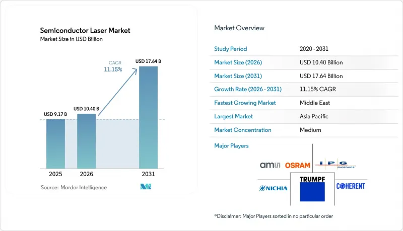
本報告按波長(紅外線雷射器、紅光雷射器、綠光雷射、藍光雷射、紫外線雷射)、雷射類型(邊發射雷射 (EEL)、垂直共振腔面射型雷射(VCSEL)、量子級聯雷射、光纖雷射)、應用領域(通訊、醫療、軍事和國防、工業、測量儀器和裝置、汽車) 5W、高於 5W)以及地區進行分類。市場預測以美元 (USD) 為單位。
全球半導體雷射器市場趨勢及洞察
家用電器中3D感測技術的快速發展
隨著智慧型手機廠商不斷擴展其臉部認證和擴增實境(AR) 功能,用於飛行時間 (ToF) 和結構光學模組的垂直腔面發射雷射 (VCSEL) 陣列的出貨量激增。這些陣列的電源效率超過 45%,並且無需主動冷卻即可在高達 150 度C 的環境下可靠運作。索尼利用其在背照式感測器方面的專業技術,將 VCSEL 晶片和 CMOS檢測器進行共封裝,從而將模組尺寸縮小了 30%,並將大批量訂單的單價控制在 2 美元以下。隨著製造商尋求確保支付功能並實現產品差異化,Android 旗艦機型的 VCSEL 採用率從 2023 年的 18% 成長到預計 2025 年的 42%。歐洲新車安全評鑑協會 (Euro NCAP) 關於車載監控的規定促使雙區 VCSEL 照明器的出現,這些照明器能夠承受 -40 度C至 +85 度C的溫度範圍,並提高了對外延均勻性的要求。穿戴式裝置也是推動市場進一步成長的重要因素,尺寸小於5毫米的VCSEL模組能夠實現手勢姿態辨識和非接觸式心率測量。預計到2028年,智慧眼鏡和健康監測器的年出貨量將超過5,000萬台。
矽光電互連領域的新需求
超大規模業者在2024年至2025年間從400G乙太網路過渡到800G以太網,將異質結III-V族雷射整合到矽晶片上,從而將每通道功耗降低到3W以下,耦合損耗降低到0.5dB以下。共封裝光學元件消除了SerDes瓶頸,並透過將雷射陣列直接放置在交換器ASIC上,將延遲降低了40ns。這在人工智慧訓練叢集中是一項極具價值的優勢。美國國防高級研究計畫局(DARPA)在2025年撥款2.03億美元,用於將異質整合良率提高到95%。目前,實際應用效率約為10%,低於風冷機架20%的熱容差要求。針對這種情況,量子點增益介質和光子晶體共振器的研究正在加緊進行,目標是到 2027 年達到 15% 的增益。克爾頻率梳正在取代離散陣列,單一微共振器可提供 80 個通道,並將都會區網路收發器組件成本降低 35%。
化合物半導體晶圓供應鏈的波動性
四家供應商控制全球78%的砷化鎵晶圓產能,使得半導體雷射市場極易受到需求劇烈波動的影響。 2023年8月,中國對鎵和鍺的出口限制導致6吋基板的前置作業時間從12週延長至26週,到2024年初,現貨價格上漲了40%。超大規模採購商已簽訂了磷化銦的長期契約,迫使規模較小的二極體製造商轉向柔軟性較低的砷化鎵替代品。雙重採購需要根據AEC-Q100和Telcordia GR-468-CORE標準進行18-24個月的檢驗,減緩了多元化採購的進程。從4吋晶圓擴大到6吋晶圓仍需要大量的資本投資,一台MOCVD反應器的成本高達400萬美元,並且需要95%的運轉率才能在五年內收回投資。
細分市場分析
到2025年,紅外線雷射將佔半導體雷射市場銷售額的42.5%,其中850nm和1550nm元件佔據消費級3D感測和長距離光纖鏈路的主導地位,為半導體雷射器市場提供支撐。儘管紫外線(UV)產品的絕對值較小,但預計到2031年,其複合年成長率將達到14.8%,這主要得益於極紫外光刻和醫用紫外線固化原型製作的出貨量成長,並且隨著先進製造工具的普及,紫外雷射器對半導體雷射器市場規模的貢獻預計也將不斷擴大。
基於VCSEL的紅外線模組可提供圓形光束,簡化耦合;而基於QCL的中紅外線光源則具備波長調諧功能,可用於氣體檢測。紫外光元件的普及仍受成本限制,但新興的266nm二極體有望帶來更高的良率和更長的使用壽命。 IEC 60825 3B類和4類等監管標準要求功率輸出超過5mW時必須採用高級互鎖裝置,這會影響設計預算和產品上市時間。隨著先進邏輯節點向3nm以下發展,微影術設備供應商預計將推動紫外光元件的需求成長,從而促進半導體雷射器市場實現兩位數成長。
透過晶圓級檢測,VCSEL成功將晶圓成本控制在0.50美元以下,從而佔據了37.8%的市場佔有率,鞏固了主導地位。同時,在中紅外紅外線監管政策的推動下,QCL正經歷快速成長,預計到2031年將以16.3%的複合年成長率成長,這表明環境和國防項目對半導體雷射器市場的規模正在產生越來越大的影響。
邊發射雷射在多千瓦工業切割領域仍佔據重要地位,但其複合年成長率僅6%,成長緩慢。光纖雷射器雖然在技術上不屬於純半導體雷射器,但由於採用二極體泵浦,其成長率維持在9%。窄線寬外共振器雷射在測量領域佔據了一席之地,該領域對線寬要求為1 MHz或更低。在預測期內,隨著汽車雷射雷達和氣體監測領域應用的不斷增加,預計垂直腔面發射雷射(VCSEL)的市場主導地位將逐漸被削弱,從而推動半導體雷射器市場收入來源的多元化。
區域分析
預計到2025年,亞太地區將佔全球收入的48.2%,這主要得益於中國在全球整體VCSEL外延晶圓市場60%的佔有率以及日本每年2億顆二極體的產量。三星的代工規模砷化鎵服務已使晶圓成本降低了20%,而印度25%的補貼政策也吸引了新的組裝。隨著新加坡、香港和東京資料中心的擴張對800Gbit收發器的需求,該地區的複合年成長率預計將達到10.8%,亞太地區預計將繼續保持其在半導體雷射器市場的中心地位。
預計到2025年,北美仍將是銷售額的重要貢獻者,這主要得益於對超大規模雲端的需求,超大規模雲佔全球矽光電出貨量的40%。儘管《晶片法案》(CHIPS Act)為國內外延晶圓生產提供了資金支持,但新晶圓廠通常需要36至48個月才能開始量產。加拿大價值1億加幣的光電叢集以及美墨加協定(USMCA)中墨西哥設備進口關稅豁免條款,正在增強北美地區的韌性。
歐洲仍是重要的收入來源,主要得益於德國通快(TRUMPF)、歐司朗(ams-OSRAM)和弗勞恩霍夫實驗室的研發投入。地平線基金會和英國的Pilotline正在加強異質整合技術,但由於認證週期長達6-12個月,RoHS和REACH法規的合規性帶來了額外的成本。中東地區12.9%的複合年成長率主要得益於NEOM公司在將LiDAR整合到行動基礎設施方面投入的5,000億美元。南美洲和非洲合計佔銷售額的6%,其中巴西是主要市場之一。
其他好處
- Excel格式的市場預測(ME)表
- 3個月的分析師支持
目錄
第1章:引言
- 研究假設和市場定義
- 調查範圍
第2章:調查方法
第3章執行摘要
第4章 市場狀況
- 市場概覽
- 市場促進因素
- 半導體雷射的應用範圍不斷擴大
- 光纖雷射應用範圍擴大
- 為什麼半導體雷射比其他光源更受歡迎
- 家用電器中3D感測技術的快速發展
- 矽光電互連領域的新需求
- 政府主導的光電製造舉措
- 市場限制因素
- 與可靠性和測試相關的挑戰
- 化合物半導體晶圓供應鏈的波動性
- 高功率下的溫度控管挑戰
- 對先進光電的嚴格出口限制
- 產業價值鏈分析
- 監理情勢
- 技術展望
- 宏觀經濟因素的影響
- 波特五力分析
第5章 市場規模與成長預測
- 波長
- 紅外線雷射
- 紅色雷射
- 綠色雷射
- 藍雷射
- 紫外線雷射
- 雷射型
- 邊發射雷射(EEL)
- 垂直共振腔面射型雷射(VCSEL)
- 量子級聯雷射
- 光纖雷射
- 其他
- 透過使用
- 溝通
- 醫學領域
- 軍事/國防
- 產業
- 測量儀器和感測器
- 車
- 其他
- 依輸出類型
- 100毫瓦或更少
- 100mW~1W
- 1W~5W
- 5瓦或以上
- 按地區
- 北美洲
- 美國
- 加拿大
- 墨西哥
- 歐洲
- 德國
- 英國
- 法國
- 義大利
- 西班牙
- 俄羅斯
- 其他歐洲國家
- 亞太地區
- 中國
- 日本
- 印度
- 韓國
- 澳洲
- 其他亞太國家
- 中東
- 沙烏地阿拉伯
- 阿拉伯聯合大公國
- 土耳其
- 其他中東國家
- 非洲
- 南非
- 奈及利亞
- 其他非洲國家
- 南美洲
- 巴西
- 阿根廷
- 南美洲其他地區
- 北美洲
第6章 競爭情勢
- 市場集中度
- 策略趨勢
- 市佔率分析
- 公司簡介
- Coherent Corp.
- Sharp Corporation
- Nichia Corporation
- IPG Photonics Corporation
- TT Electronics plc
- Sumitomo Electric Industries Ltd.
- Sheaumann Laser Inc.
- Newport Corporation(MKS Instruments Inc.)
- Panasonic Industry Co. Ltd.
- Rohm Co. Ltd.
- Hamamatsu Photonics KK
- Jenoptik AG
- TRUMPF Group
- ams-OSRAM AG
- Lumentum Holdings Inc.
- Broadcom Inc.
- Furukawa Electric Co. Ltd.
- Innolume GmbH
- MACOM Technology Solutions Holdings Inc.
- II-VI 公司(現為 Coherent 的子公司)
第7章 市場機會與未來展望
According to Mordor Intelligence, the semiconductor laser market size is expected to increase from USD 9.17 billion in 2025 to USD 10.40 billion in 2026 and reach USD 17.64 billion by 2031, growing at a CAGR of 11.15% over 2026-2031.
This report is Segmented by Wavelength (Infrared, Red, Green, Blue, and Ultraviolet), Laser Type (Edge-Emitting, VCSEL, Quantum Cascade, and Fiber), Application (Communication, Medical, Military and Defense, Industrial, Instrumentation and Sensor, and Automotive), Power Output (Below 100 MW, 100 MW To 1 W, 1 W To 5 W, and Above 5 W), and Geography. Market Forecasts are in Value (USD).
Global Semiconductor Laser Market Trends and Insights
Rapid Expansion of 3D Sensing in Consumer Electronics
VCSEL array shipments for time-of-flight and structured-light modules surged as smartphone vendors broadened facial authentication and augmented-reality features, with wall-plug efficiencies topping 45% and reliable operation up to 150 °C without active cooling . Sony leveraged its back-illuminated sensor expertise to co-package VCSEL dies and CMOS detectors, reducing module footprints by 30% and lowering unit costs to below USD 2 in high-volume orders. Android flagship adoption increased from 18% in 2023 to an estimated 42% in 2025, as manufacturers sought to secure payments and differentiate their products. Euro NCAP cabin-monitoring rules triggered dual-zone VCSEL illuminators that withstand temperatures ranging from -40 °C to +85 °C, thereby tightening epitaxial uniformity requirements. Wearables add another growth vector, with smart glasses and health monitors forecast to exceed 50 million units annually by 2028 as sub-5 mm VCSEL modules enable gesture recognition and non-contact heart-rate sensing.
Emerging Demand from Silicon Photonics Interconnects
Hyperscale operators transitioned from 400G to 800G Ethernet between 2024 and 2025, integrating heterogeneously bonded III-V lasers on silicon to achieve sub-3W lane power and coupling losses of below 0.5 dB. Co-packaged optics place laser arrays directly on switch ASICs, eliminating SerDes bottlenecks and cutting latency by 40 ns, an edge prized for AI training clusters. DARPA committed USD 203 million in 2025 to lift heterogeneous integration yields toward 95%. The current wall-plug efficiency hovers near 10%, falling short of the 20% thermal envelope for air-cooled racks, which has spurred research on quantum-dot gain media and photonic-crystal cavities aimed at achieving 15% by 2027. Kerr frequency combs are displacing discrete arrays, providing 80 channels from one micro-resonator and reducing transceiver bills of materials by 35% in metro networks.
Supply Chain Volatility of Compound Semiconductor Wafers
Four suppliers control 78% of global gallium-arsenide wafer capacity, leaving the semiconductor laser market exposed to sudden demand swings. China's August 2023 curbs on gallium and germanium stretched 6-inch substrate lead times from 12 to 26 weeks and pushed spot prices 40% higher by early 2024. Hyperscale buyers locked long-term indium-phosphide contracts, crowding smaller diode makers toward less flexible gallium-arsenide alternatives. Dual-sourcing requires 18-24 months of AEC-Q100 and Telcordia GR-468-CORE testing, which delays diversification. Scaling from 4- to 6-inch wafers remains capital-intensive; a single MOCVD reactor costs USD 4 million and needs 95% utilization for a 5-year payback.
Other drivers and restraints analyzed in the detailed report include:
- Proliferation of Semiconductor Laser Applications
- Government-Backed Photonics Manufacturing Initiatives
- Thermal Management Challenges at High Power Outputs
For complete list of drivers and restraints, kindly check the Table Of Contents.
Segment Analysis
Infrared lasers accounted for 42.5% of 2025 revenue, underpinning the semiconductor laser market through 850 nm and 1,550 nm devices that dominate consumer 3D sensing and long-haul fiber links . Ultraviolet variants, although smaller in absolute dollars, will climb at a 14.8% CAGR to 2031 on EUV lithography shipments and medical UV-curable prototyping, pointing to a rising semiconductor laser market size contribution from advanced manufacturing tools.
VCSEL-based infrared modules deliver circular beams that simplify coupling, while QCL-based mid-infrared sources provide tunability for gas sensing. Ultraviolet penetration remains cost-sensitive but emerging 266 nm diodes promise higher yields and longer lifetimes. Regulatory IEC 60825 Class 3B and Class 4 limits demand sophisticated interlocks above 5 mW, influencing design budgets and time to market. As advanced logic nodes migrate below 3 nm, lithography tool vendors will propel ultraviolet demand, reinforcing its double-digit climb within the semiconductor laser market.
VCSELs captured a 37.8% share, thanks to wafer-scale testing that reduces die cost below USD 0.50, thereby safeguarding their leadership in the semiconductor laser market. QCLs, however, are racing ahead at a 16.3% CAGR through 2031, as mid-infrared spectroscopy gains regulatory tailwinds, suggesting a growing impact on the semiconductor laser market size from environmental and defense programs.
Edge-emitting bars retain relevance for multi-kilowatt industrial cutting, yet their 6% CAGR lags. Fiber lasers, although technically outside the pure semiconductor classification, depend on diode pumping and maintain a 9% trajectory. Narrow-linewidth external-cavity diodes fill metrology niches requiring <1 MHz linewidth. Over the forecast period, design wins in automotive LiDAR and gas monitoring will help QCLs erode VCSEL dominance, diversifying revenue streams within the semiconductor laser market.
Complete Report Scope:
- By Wavelength
- Infrared Lasers
- Red Lasers
- Green Lasers
- Blue Lasers
- Ultraviolet Lasers
- By Laser Type
- Edge-Emitting Lasers (EEL)
- Vertical-Cavity Surface-Emitting Lasers (VCSEL)
- Quantum Cascade Lasers
- Fiber Lasers
- Other Types
- By Application
- Communication
- Medical
- Military and Defense
- Industrial
- Instrumentation and Sensor
- Automotive
- Other Applications
- By Power Output
- Below 100 mW
- 100 mW - 1 W
- 1 W - 5 W
- Above 5 W
- By Geography
- North America
- United States
- Canada
- Mexico
- Europe
- Germany
- United Kingdom
- France
- Italy
- Spain
- Russia
- Rest of Europe
- Asia-Pacific
- China
- Japan
- India
- South Korea
- Australia
- Rest of Asia-Pacific
- Middle East
- Saudi Arabia
- United Arab Emirates
- Turkey
- Rest of Middle East
- Africa
- South Africa
- Nigeria
- Rest of Africa
- South America
- Brazil
- Argentina
- Rest of South America
- North America
Geography Analysis
The Asia-Pacific region generated 48.2% of 2025 revenue, reflecting China's 60% share of global VCSEL epitaxial wafers and Japan's 200 million-unit annual diode output. Samsung's foundry-scale gallium-arsenide services trim wafer costs by 20%, while India's 25% subsidy attracts new assembly lines. Singapore, Hong Kong, and Tokyo data center expansions, which require 800 Gbit transceivers, are expected to support a 10.8% regional CAGR, keeping the Asia-Pacific region central to the semiconductor laser market.
North America remained a significant contributor to 2025 sales, driven by hyperscale cloud consumption, which comprises 40% of global silicon photonics shipments. The CHIPS Act will fund domestic epitaxial wafers; however, new fabs typically require 36 to 48 months to reach volume production. Canada's CAD 100 million photonics cluster and Mexico's duty-free equipment imports under USMCA strengthen continental resilience.
Europe remained a significant revenue contributor, anchored by Germany's TRUMPF and ams-OSRAM plus Fraunhofer R&D. Horizon funds and UK pilot lines enhance heterogeneous integration, while RoHS and REACH compliance add six-to-twelve-month qualification overhead. The Middle East's 12.9% CAGR is driven by NEOM's USD 500 billion investment, which incorporates LiDAR into mobility infrastructure. South America and Africa together supply 6% of the revenue, with Brazil's.
- Coherent Corp.
- Sharp Corporation
- Nichia Corporation
- IPG Photonics Corporation
- TT Electronics plc
- Sumitomo Electric Industries Ltd.
- Sheaumann Laser Inc.
- Newport Corporation (MKS Instruments Inc.)
- Panasonic Industry Co. Ltd.
- Rohm Co. Ltd.
- Hamamatsu Photonics K.K.
- Jenoptik AG
- TRUMPF Group
- ams-OSRAM AG
- Lumentum Holdings Inc.
- Broadcom Inc.
- Furukawa Electric Co. Ltd.
- Innolume GmbH
- MACOM Technology Solutions Holdings Inc.
- II-VI Incorporated (now part of Coherent)
Additional Benefits:
- The market estimate (ME) sheet in Excel format
- 3 months of analyst support
TABLE OF CONTENTS
1 INTRODUCTION
- 1.1 Study Assumptions and Market Definition
- 1.2 Scope of the Study
2 RESEARCH METHODOLOGY
3 EXECUTIVE SUMMARY
4 MARKET LANDSCAPE
- 4.1 Market Overview
- 4.2 Market Drivers
- 4.2.1 Proliferation of Semiconductor Laser Applications
- 4.2.2 Growth in Fiber Laser Adoption
- 4.2.3 Preference for Semiconductor Lasers over Other Light Sources
- 4.2.4 Rapid Expansion of 3D Sensing in Consumer Electronics
- 4.2.5 Emerging Demand from Silicon Photonics Interconnects
- 4.2.6 Government-Backed Photonics Manufacturing Initiatives
- 4.3 Market Restraints
- 4.3.1 Difficulties Regarding Reliability and Testing
- 4.3.2 Supply Chain Volatility of Compound Semiconductor Wafers
- 4.3.3 Thermal Management Challenges at High Power Outputs
- 4.3.4 Stringent Export Controls on Advanced Photonics
- 4.4 Industry Value Chain Analysis
- 4.5 Regulatory Landscape
- 4.6 Technological Outlook
- 4.7 Impact of Macroeconomic Factors
- 4.8 Porter's Five Forces Analysis
- 4.8.1 Threat of New Entrants
- 4.8.2 Bargaining Power of Suppliers
- 4.8.3 Bargaining Power of Buyers
- 4.8.4 Threat of Substitutes
- 4.8.5 Competitive Rivalry
5 MARKET SIZE AND GROWTH FORECASTS (VALUE)
- 5.1 By Wavelength
- 5.1.1 Infrared Lasers
- 5.1.2 Red Lasers
- 5.1.3 Green Lasers
- 5.1.4 Blue Lasers
- 5.1.5 Ultraviolet Lasers
- 5.2 By Laser Type
- 5.2.1 Edge-Emitting Lasers (EEL)
- 5.2.2 Vertical-Cavity Surface-Emitting Lasers (VCSEL)
- 5.2.3 Quantum Cascade Lasers
- 5.2.4 Fiber Lasers
- 5.2.5 Other Types
- 5.3 By Application
- 5.3.1 Communication
- 5.3.2 Medical
- 5.3.3 Military and Defense
- 5.3.4 Industrial
- 5.3.5 Instrumentation and Sensor
- 5.3.6 Automotive
- 5.3.7 Other Applications
- 5.4 By Power Output
- 5.4.1 Below 100 mW
- 5.4.2 100 mW - 1 W
- 5.4.3 1 W - 5 W
- 5.4.4 Above 5 W
- 5.5 By Geography
- 5.5.1 North America
- 5.5.1.1 United States
- 5.5.1.2 Canada
- 5.5.1.3 Mexico
- 5.5.2 Europe
- 5.5.2.1 Germany
- 5.5.2.2 United Kingdom
- 5.5.2.3 France
- 5.5.2.4 Italy
- 5.5.2.5 Spain
- 5.5.2.6 Russia
- 5.5.2.7 Rest of Europe
- 5.5.3 Asia-Pacific
- 5.5.3.1 China
- 5.5.3.2 Japan
- 5.5.3.3 India
- 5.5.3.4 South Korea
- 5.5.3.5 Australia
- 5.5.3.6 Rest of Asia-Pacific
- 5.5.4 Middle East
- 5.5.4.1 Saudi Arabia
- 5.5.4.2 United Arab Emirates
- 5.5.4.3 Turkey
- 5.5.4.4 Rest of Middle East
- 5.5.5 Africa
- 5.5.5.1 South Africa
- 5.5.5.2 Nigeria
- 5.5.5.3 Rest of Africa
- 5.5.6 South America
- 5.5.6.1 Brazil
- 5.5.6.2 Argentina
- 5.5.6.3 Rest of South America
- 5.5.1 North America
6 COMPETITIVE LANDSCAPE
- 6.1 Market Concentration
- 6.2 Strategic Moves
- 6.3 Market Share Analysis
- 6.4 Company Profiles (includes Global level Overview, Market level overview, Core Segments, Financials as available, Strategic Information, Market Rank/Share for key companies, Products and Services, and Recent Developments)
- 6.4.1 Coherent Corp.
- 6.4.2 Sharp Corporation
- 6.4.3 Nichia Corporation
- 6.4.4 IPG Photonics Corporation
- 6.4.5 TT Electronics plc
- 6.4.6 Sumitomo Electric Industries Ltd.
- 6.4.7 Sheaumann Laser Inc.
- 6.4.8 Newport Corporation (MKS Instruments Inc.)
- 6.4.9 Panasonic Industry Co. Ltd.
- 6.4.10 Rohm Co. Ltd.
- 6.4.11 Hamamatsu Photonics K.K.
- 6.4.12 Jenoptik AG
- 6.4.13 TRUMPF Group
- 6.4.14 ams-OSRAM AG
- 6.4.15 Lumentum Holdings Inc.
- 6.4.16 Broadcom Inc.
- 6.4.17 Furukawa Electric Co. Ltd.
- 6.4.18 Innolume GmbH
- 6.4.19 MACOM Technology Solutions Holdings Inc.
- 6.4.20 II-VI Incorporated (now part of Coherent)
7 MARKET OPPORTUNITIES AND FUTURE OUTLOOK
- 7.1 White-Space and Unmet-Need Assessment

 磷化銦雷射積體電路市場分析與預測(至2035年):類型、產品類型、技術、組件、應用、材料類型、裝置、製程、最終用戶、功能
 2026年全球半導體雷射器市場報告
 半導體雷射器市場機會、成長要素、產業趨勢分析及2026-2035年預測。
 電吸收調變器市場:運行原理、波導管結構、波段、應用和最終用戶分類-2026-2032年全球市場預測半導體雷射器市場分析及預測(至2035年):類型、產品類型、技術、組件、應用、材料類型、製程、最終用戶、功能、振盪模式半導體雷射市場:依發射結構、結構、半導體材料、波長頻寬、工作模式、光纖耦合、應用和銷售管道分類-2026-2032年全球預測
 半導體雷射器市場規模、佔有率、成長及全球產業分析:按類型、應用和地區的洞察,2026-2034年的預測多層半導體雷射市場:按雷射類型、波長、工作模式、功率輸出和應用分類-全球預測,2026-2032年固體半導體雷射感測市場分析及至2035年的預測:依類型、產品、技術、組件、應用、材料類型、最終用戶、功能、安裝類型及解決方案分類
 電吸收調製雷射 (EML) - 全球市場佔有率和排名、總收入和需求預測(2026-2032 年)