


 |
市場調查報告書
商品編碼
2122664
NAND快閃記憶體:市場佔有率分析、產業趨勢與統計資料、成長預測(2026-2031年)NAND Flash Memory - Market Share Analysis, Industry Trends & Statistics, Growth Forecasts (2026 - 2031) |
||||||

※ 本網頁內容可能與最新版本有所差異。詳細情況請與我們聯繫。
根據 Mordor Intelligence 估計,2026 年NAND快閃記憶體體市值將達到 586.9 億美元,高於 2025 年的 557.3 億美元,預計到 2031 年將達到 760.3 億美元。
預計從 2026 年到 2031 年,其複合年成長率將達到 5.32%。
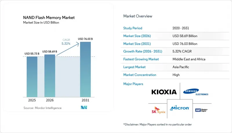
本報告依類型(SLC(單層單元)、MLC(多層單元)、TLC(三層單元)、QLC(四層單元))、結構(2D(平面)NAND、3D NAND)、介面(SATA、PCIe/NVMe、UFS/eMMC)、應用程式(智慧型手機、固態硬碟(PC/遊戲機)、企業/其他地區進行資料區/區域/電腦)、企業/機組進行系統/版圖、3////////eMMC)。市場預測以美元計價。
全球NAND快閃記憶體體市場趨勢及洞察
資料中心人工智慧/機器學習儲存的激增
超大規模營運商正在重新設計其儲存層級,將NVMe SSD池部署在更靠近GPU叢集的位置,從而為搜尋、擴展和產生工作負載保持每秒千兆位元組的吞吐量。西部數據預計,到2029年,僅5G終端的NAND閃存累積需求就將達到Petabyte,這凸顯了閃存在彌合內存和冷藏保管之間性能差距方面的重要性。採購藍圖正日益優先考慮30TB至100TB的企業級硬碟,三星將於2024年發布的128TB BM1743 SSD就體現了這一轉變。由此產生的連鎖反應正在加速層數創新和控制器級壓縮技術的發展,從而推動NAND快閃記憶體快閃記憶體市場持續成長。
5G和大規模物聯網設備的普及
獨立組網5G的部署將推動邊緣分析、智慧工廠、聯網汽車和智慧電網等應用場景的發展,而這些應用都需要本地非揮發性儲存來支援即時決策引擎。西部數據發布的白皮書預測,一旦儲存容量超過8GB,工業級模組將出現從NOR快閃記憶體向NAND快閃記憶體的轉變。半導體產業的發展藍圖目前優先考慮寬溫域QLC晶片和車規級NVMe設計,這將使NAND快閃記憶體市場在交通運輸和基礎設施領域佔據更大的佔有率。
高密度電池的耐久極限
QLC快閃記憶體1000-3000次的寫入/擦除循環次數閾值對於擁有龐大日誌量的資料庫而言仍然不足,迫使用戶過度配置,從而削弱了成本效益。 Hackaday指出,隨著300層堆疊中電子陷阱的磨損加速,物理極限正在逼近。雖然先進的糾錯和損耗均衡演算法可以緩解劣化,但PLC和交叉點等替代記憶體仍處於發展階段,並且在它們的耐久性得到驗證之前,可能會繼續限制NAND快閃記憶體快閃記憶體市場的一部分佔有率。
細分市場分析
由於TLC裝置在耐用性和成本方面實現了卓越的平衡,因此在NAND快閃記憶體市場佔據了63.58%的佔有率。同時,QLC正以6.35%的複合年成長率快速成長,這主要得益於超大規模資料中心業者中心在AI資料湖中展現出的8-16倍的密度優勢。預計到2031年,QLC在NAND快閃記憶體快閃記憶體市場的整體佔有率將進一步提升。三星的280層QLC原型藍圖應用於16TB單面M.2固態硬碟,在滿足推理叢集處理容量要求的同時,還能減少機架面積。控制器級SLC快取技術和片上ECC技術正在縮小與TLC的延遲差距,從而促進包括視訊點播庫和備份儲存庫在內的各種工作負載的遷移。 TLC預計將在寫入密集型ERP和OLTP環境中保持其優勢,因為超過10,000次的壽命能夠確保可預測的服務品質。
儘管TLC優異的功耗特性使其在消費級筆記型電腦領域保持領先地位,但QLC每比特成本的不斷下降已對中階產品構成壓力。美光第六代QLC相比第一代產品,讀取延遲降低了34%,縮小了先前人們認為的效能差距。隨著基於韌體的生命週期管理技術的日益成熟,OEM廠商可能會採用分級產品線,在高容量產品中使用QLC,並在高階產品線中繼續採用先進的TLC製程。這種相互作用表明,在預測期內,這兩種技術都將繼續在NAND快閃記憶體市場佔據核心地位。
從平面結構到垂直堆疊結構的過渡已基本完成,預計到2025年,3D NAND將佔據NAND快閃記憶體市場86.85%的佔有率。堆疊層數的顯著提升,例如SK海力士的商用321層TLC和三星的400層以上的V-NAND,顯示在本十年末之前,堆疊層數將穩步突破500層大關。其合理性顯而易見:垂直堆疊可以在不減小單元尺寸的情況下提高容量,並繞過微影術的限制。 2D NAND則主要應用於航太和國防等細分領域,在這些領域,超低延遲寫入比容量更為重要。
增加層數會增加互連電阻和單元間干擾。為了克服這個問題,鎧俠(Kioxia)的CMOS鍵結陣列策略透過隔離外圍電路,提高了超高堆疊結構的I/O效率和良率。三星(Samsung)對用於奶油狀界面柵極的氧化鉿鐵電的研究也旨在實現類似的目標:即使堆疊高度增加,也能保持閾值電壓裕度。
區域分析
預計到2025年,亞太地區將佔全球NAND快閃記憶體銷售額的55.40%,其中韓國垂直整合的巨頭企業和中國龐大的設備組裝中心是其核心。三星第九代V-NAND(286層)的量產以及SK海力士321層TLC生產線的投產,凸顯了該地區的技術優勢。總部位於北京的國內巨頭長江儲存(YMTC)不顧出口限制,正大力推動232層QLC製程的研發,展現了國內主導的產能擴張,這將鞏固亞太地區在NAND快閃記憶體快閃記憶體市場的主導地位。
北美地區銷售額位居第二,主要得益於雲端運算領域的強勁資本投資。 《晶片與科學法案》正在資助美光公司斥資1,250億美元在美國建設計畫,旨在2035年提高美國在先進記憶體領域的自給自足能力。加拿大正在提供控制器IP設計人才,而墨西哥則在美墨加協定(USMCA)的框架下擴大其模組級組裝線,所有這些國家都在共同努力,以加強區域供應鏈的多元化。
由於儲存晶圓製造能力的限制,歐洲的市佔率仍維持在個位數中段。然而,德國和法國的汽車及工業OEM廠商對車用NVMe模組的需求強勁。諸如「歐洲綠色交易」等永續性指令正促使買家轉向節能型PCIe 5.0 SSD,以降低機架能耗密度。歐洲晶圓廠正致力於透過新一代3D NAND節點搶佔此細分市場的佔有率,這些節點每次讀取的能耗低於3 pJ/bit。
中東和非洲地區以8.21%的複合年成長率呈現最高成長率。沙烏地阿拉伯的「2030願景」正在推動利雅德周邊地區從晶圓到後端一體化產業鏈的建設,而阿布達比的政府投資者則在探索與專業控制器公司成立合資企業,以促進區域供應鏈的發展。豐富的可再生能源開發專案和極具吸引力的稅收優惠政策正在吸引封裝合作夥伴,在地化生產的基礎正在奠定,旨在提升海灣合作理事會(GCC)成員國資料中心市場對NAND快閃記憶體的滲透率。
其他好處
- Excel格式的市場預測(ME)表
- 3個月的分析師支持
目錄
第1章:引言
- 研究假設和市場定義
- 調查範圍
第2章:調查方法
第3章執行摘要
第4章 市場狀況
- 市場概覽
- 市場促進因素
- 資料中心對人工智慧/機器學習儲存的需求激增
- 5G和大規模物聯網設備的普及
- PC 和遊戲機中從 HDD 到 SSD 的遷移
- 企業正遷移到性價比更高的QLC固態硬碟。
- 國內陸NAND快閃記憶體晶片製造項目
- 實現與 CXL 相容的計算存儲
- 市場限制因素
- 高密度電池耐久性的極限
- 價格週期性和資本投資負擔
- 由於出口限制導致設備供不應求
- 對高階製造實驗室永續性的審查
- 工業供應鏈分析
- 監理情勢
- 技術展望
- 宏觀經濟因素的影響
- 波特五力分析
第5章 市場規模與成長預測
- 按類型
- SLC(單層單元)
- MLC(多層細胞)
- TLC(三層板)
- QLC(四層池)
- 按結構
- 2D(平面)NAND
- 3D NAND
- 透過介面
- SATA
- PCIe/NVMe
- UFS/eMMC
- 透過使用
- 智慧型手機
- 固態硬碟(PC/遊戲機)
- 企業/資料中心用固態硬碟
- 記憶卡和USB
- 工業和汽車電子設備
- 按地區
- 北美洲
- 美國
- 加拿大
- 墨西哥
- 南美洲
- 巴西
- 阿根廷
- 其他南美國家
- 歐洲
- 德國
- 英國
- 法國
- 義大利
- 西班牙
- 俄羅斯
- 其他歐洲國家
- 亞太地區
- 中國
- 日本
- 印度
- 韓國
- 東南亞
- 其他亞太國家
- 中東和非洲
- 中東
- 沙烏地阿拉伯
- 阿拉伯聯合大公國
- 土耳其
- 其他中東國家
- 非洲
- 南非
- 奈及利亞
- 其他非洲地區
- 中東
- 北美洲
第6章 競爭情勢
- 市場集中度
- 策略趨勢
- 市佔率分析
- 公司簡介
- Samsung Electronics Co., Ltd.
- SK hynix Inc.
- KIOXIA Holdings Corporation
- Western Digital Corporation
- Micron Technology, Inc.
- Nanya Technology Corporation
- Powerchip Technology Corporation
- Winbond Electronics Corporation
- Macronix International Co., Ltd.
- Silicon Motion Technology Corp.
- Phison Electronics Corp.
- Kingston Technology Company, Inc.
- ADATA Technology Co., Ltd.
- Transcend Information, Inc.
- GigaDevice Semiconductor Inc.
- SK Group(Solid-State Storage division)
- PNY Technologies, Inc.
- Team Group Inc.
- Longsys Electronics Co., Ltd.
- Smart Modular Technologies, Inc.
第7章 市場機會與未來展望
According to Mordor Intelligence, NAND flash memory market size in 2026 is estimated at USD 58.69 billion, growing from 2025 value of USD 55.73 billion with 2031 projections showing USD 76.03 billion, growing at 5.32% CAGR over 2026-2031.
This report is Segmented by Type (SLC (Single-Level Cell), MLC (Multi-Level Cell), TLC (Triple-Level Cell), and QLC (Quad-Level Cell)), Structure (2D (Planar) NAND, and 3D NAND), Interface (SATA, Pcie / NVMe, and UFS / EMMC), Application (Smartphones, Solid-State Drives (PC and Console), Enterprise / Data-Center SSD, and More), and Geography. The Market Forecasts are Provided in Terms of Value (USD).
Global NAND Flash Memory Market Trends and Insights
Data-center AI/ML storage surge
Hyperscale operators are redesigning storage hierarchies so that NVMe SSD pools sit closer to GPU clusters, sustaining multi-gigabyte-per-second throughput for retrieval-augmented generation workloads. Western Digital estimates cumulative demand of 19,000 petabytes of NAND by 2029 for 5G-enabled endpoints alone, underscoring flash's role in bridging memory and cold-storage performance gaps. Procurement roadmaps increasingly favor 30 TB to 100 TB enterprise drives, a shift visible in Samsung's 128 TB BM1743 SSD showcased in 2024. The resulting pull-through effect accelerates layer-count innovation and controller-level compression techniques that sustain the NAND flash memory market momentum.
5G and massive-IoT device proliferation
Standalone 5G deployments unlock edge analytics use cases, smart factories, connected cars, and smart grids that mandate local non-volatile storage for real-time decision engines. Western Digital's white paper anticipates a NOR-to-NAND crossover within industrial modules as capacities climb above 8 GB. Semiconductor roadmaps now prioritize extended-temperature QLC die and automotive-qualified NVMe designs, broadening the NAND flash memory market footprint across transportation and infrastructure domains.
Endurance limits of high-density cells
QLC's 1,000-3,000 program/erase thresholds remain insufficient for log-heavy databases, forcing over-provisioning that erodes cost benefits. Hackaday notes the physics ceiling approaching as electron-trap wear accelerates in 300-layer stacks. Although advanced error-correction and wear-leveling algorithms offset degradation, alternate memories such as PLC or cross-point remain on the horizon, tempering portions of the NAND flash memory market until longevity is proven.
Other drivers and restraints analyzed in the detailed report include:
- PC/Console transition from HDD to SSD
- Enterprise pivot to cost-efficient QLC SSDs
- Pricing cyclicality and cap-ex burden
For complete list of drivers and restraints, kindly check the Table Of Contents.
Segment Analysis
The NAND flash memory market size for TLC devices held a 63.58% market share with the strength of balanced endurance and cost. QLC, however, is accelerating at 6.35% CAGR as hyperscalers validate its 8-16X density advantage for AI data-lakes, which lifts the overall NAND flash memory market share allocated to QLC by 2031. Samsung's 280-layer QLC prototype signals a roadmap to 16 TB single-sided M.2 drives, shrinking rack footprints while meeting throughput rules for inference clusters. Controller-level SLC-cache techniques and on-die ECC are narrowing the latency gap with TLC, encouraging broader workloads such as VOD libraries and backup repositories to migrate. TLC will retain primacy in write-intensive ERP and OLTP environments where its 10,000-plus cycle rating secures predictable quality-of-service.
In consumer notebooks, TLC's favorable power profile sustains its install base, but falling QLC cost-per-bit is already pressuring mid-range SKUs. Micron's sixth-gen QLC exhibits 34% lower read latency than first-gen samples, eroding the perceived performance divide. As firmware-defined endurance mitigation matures, OEMs will likely introduce tiered offerings where high-capacity SKUs employ QLC, while premium lines continue on advanced TLC nodes. This interplay keeps both technologies central to the NAND flash memory market over the forecast horizon.
The shift from planar to vertical stacking is virtually complete: 3D NAND commanded 86.85% of the NAND flash memory market share in 2025. Layer-count breakthroughs, SK Hynix's commercial 321-layer TLC and Samsung's 400-plus-layer V-NAND, signal confident scaling beyond the 500-layer watermark before decade-end. The economic logic is clear; vertical scaling adds capacity without shrinking cell size, sidestepping lithography constraints. 2D NAND survives in niche aerospace and defense modules where ultra-low-latency writes outweigh capacity.
Layer additions do stress interconnect resistance and cell-to-cell interference. To overcome this, Kioxia's CMOS-bonded-array strategy decouples peripheral circuits, boosting I/O efficiency and improving yield in ultra-tall stacks. Samsung's exploration of hafnia ferroelectrics for creamy-interface gates pursues a similar aim: maintain threshold-voltage margins even as stack height extends.
Complete Report Scope:
- By Type
- SLC (Single-Level Cell)
- MLC (Multi-Level Cell)
- TLC (Triple-Level Cell)
- QLC (Quad-Level Cell)
- By Structure
- 2D (Planar) NAND
- 3D NAND
- By Interface
- SATA
- PCIe / NVMe
- UFS / eMMC
- By Application
- Smartphones
- Solid-State Drives (PC and Console)
- Enterprise / Data-center SSD
- Memory Cards and USB Drives
- Industrial and Automotive Electronics
- By Geography
- North America
- United States
- Canada
- Mexico
- South America
- Brazil
- Argentina
- Rest of South America
- Europe
- Germany
- United Kingdom
- France
- Italy
- Spain
- Russia
- Rest of Europe
- Asia-Pacific
- China
- Japan
- India
- South Korea
- South-East Asia
- Rest of Asia-Pacific
- Middle East and Africa
- Middle East
- Saudi Arabia
- United Arab Emirates
- Turkey
- Rest of Middle East
- Africa
- South Africa
- Nigeria
- Rest of Africa
- Middle East
- North America
Geography Analysis
Asia-Pacific contributed 55.40% of sales in 2025, anchored by South Korea's vertically-integrated champions and China's colossal device assembly base. Samsung's mass production of 9th-generation V-NAND (286 layers) and SK Hynix's 321-layer TLC line affirm the region's technology lead. Beijing's domestic champion YMTC pushes 232-layer QLC nodes despite export-control constraints, illustrating indigenous capacity expansion that preserves Asia-Pacific's outsized influence on the NAND flash memory market.
North America sits second on revenue league tables, propelled by cloud capital-expenditure intensity. The CHIPS and Science Act bankrolls Micron's USD 125 billion state-side megafab roadmap, lifting U.S. advanced-memory self-sufficiency by 2035. Canada contributes controller-IP design talent, while Mexico scales module-level assembly lines under USMCA provisions, together reinforcing regional supply diversification.
Europe registers mid-single-digit share, constrained by limited memory wafer fabrication. Nonetheless, automotive and industrial OEMs in Germany and France generate robust demand for auto-grade NVMe modules. Sustainability directives such as the European Green Deal pivot buyers toward power-efficient PCIe 5.0 SSDs that lower rack energy density, a niche European fabs aim to capture through next-generation 3D NAND nodes with under-3 pJ/bit read energy footprints.
The Middle East and Africa present the highest growth rate at 8.21% CAGR. Saudi Arabia's Vision 2030 underwrites wafer-to-back-end complexes around Riyadh, while Abu Dhabi's sovereign investors explore joint-ventures with controller specialists to bootstrap a regional supply chain. Ample renewable-energy pipelines and attractive tax regimes draw packaging partners, setting the stage for localized production that boosts the NAND flash memory market penetration across GCC data hubs.
- Samsung Electronics Co., Ltd.
- SK hynix Inc.
- KIOXIA Holdings Corporation
- Western Digital Corporation
- Micron Technology, Inc.
- Nanya Technology Corporation
- Powerchip Technology Corporation
- Winbond Electronics Corporation
- Macronix International Co., Ltd.
- Silicon Motion Technology Corp.
- Phison Electronics Corp.
- Kingston Technology Company, Inc.
- ADATA Technology Co., Ltd.
- Transcend Information, Inc.
- GigaDevice Semiconductor Inc.
- SK Group (Solid-State Storage division)
- PNY Technologies, Inc.
- Team Group Inc.
- Longsys Electronics Co., Ltd.
- Smart Modular Technologies, Inc.
Additional Benefits:
- The market estimate (ME) sheet in Excel format
- 3 months of analyst support
TABLE OF CONTENTS
1 INTRODUCTION
- 1.1 Study Assumptions and Market Definition
- 1.2 Scope of the Study
2 RESEARCH METHODOLOGY
3 EXECUTIVE SUMMARY
4 MARKET LANDSCAPE
- 4.1 Market Overview
- 4.2 Market Drivers
- 4.2.1 Data-center AI/ML storage surge
- 4.2.2 5G and massive-IoT device proliferation
- 4.2.3 PC/Console transition from HDD to SSD
- 4.2.4 Enterprise pivot to cost-efficient QLC SSDs
- 4.2.5 National on-shore NAND fab programs
- 4.2.6 CXL-enabled computational storage adoption
- 4.3 Market Restraints
- 4.3.1 Endurance limits of high-density cells
- 4.3.2 Pricing cyclicality and cap-ex burden
- 4.3.3 Export-control induced equipment bottlenecks
- 4.3.4 Sustainability scrutiny on high-layer fabs
- 4.4 Industry Supply Chain Analysis
- 4.5 Regulatory Landscape
- 4.6 Technological Outlook
- 4.7 Impact of Macroeconomic Factors
- 4.8 Porter's Five Forces Analysis
- 4.8.1 Bargaining Power of Suppliers
- 4.8.2 Bargaining Power of Buyers
- 4.8.3 Threat of New Entrants
- 4.8.4 Threat of Substitutes
- 4.8.5 Intensity of Competitive Rivalry
5 MARKET SIZE AND GROWTH FORECASTS (VALUE)
- 5.1 By Type
- 5.1.1 SLC (Single-Level Cell)
- 5.1.2 MLC (Multi-Level Cell)
- 5.1.3 TLC (Triple-Level Cell)
- 5.1.4 QLC (Quad-Level Cell)
- 5.2 By Structure
- 5.2.1 2D (Planar) NAND
- 5.2.2 3D NAND
- 5.3 By Interface
- 5.3.1 SATA
- 5.3.2 PCIe / NVMe
- 5.3.3 UFS / eMMC
- 5.4 By Application
- 5.4.1 Smartphones
- 5.4.2 Solid-State Drives (PC and Console)
- 5.4.3 Enterprise / Data-center SSD
- 5.4.4 Memory Cards and USB Drives
- 5.4.5 Industrial and Automotive Electronics
- 5.5 By Geography
- 5.5.1 North America
- 5.5.1.1 United States
- 5.5.1.2 Canada
- 5.5.1.3 Mexico
- 5.5.2 South America
- 5.5.2.1 Brazil
- 5.5.2.2 Argentina
- 5.5.2.3 Rest of South America
- 5.5.3 Europe
- 5.5.3.1 Germany
- 5.5.3.2 United Kingdom
- 5.5.3.3 France
- 5.5.3.4 Italy
- 5.5.3.5 Spain
- 5.5.3.6 Russia
- 5.5.3.7 Rest of Europe
- 5.5.4 Asia-Pacific
- 5.5.4.1 China
- 5.5.4.2 Japan
- 5.5.4.3 India
- 5.5.4.4 South Korea
- 5.5.4.5 South-East Asia
- 5.5.4.6 Rest of Asia-Pacific
- 5.5.5 Middle East and Africa
- 5.5.5.1 Middle East
- 5.5.5.1.1 Saudi Arabia
- 5.5.5.1.2 United Arab Emirates
- 5.5.5.1.3 Turkey
- 5.5.5.1.4 Rest of Middle East
- 5.5.5.2 Africa
- 5.5.5.2.1 South Africa
- 5.5.5.2.2 Nigeria
- 5.5.5.2.3 Rest of Africa
- 5.5.5.1 Middle East
- 5.5.1 North America
6 COMPETITIVE LANDSCAPE
- 6.1 Market Concentration
- 6.2 Strategic Moves
- 6.3 Market Share Analysis
- 6.4 Company Profiles (includes Global level Overview, Market level overview, Core Segments, Financials as available, Strategic Information, Market Rank/Share for key companies, Products and Services, and Recent Developments)
- 6.4.1 Samsung Electronics Co., Ltd.
- 6.4.2 SK hynix Inc.
- 6.4.3 KIOXIA Holdings Corporation
- 6.4.4 Western Digital Corporation
- 6.4.5 Micron Technology, Inc.
- 6.4.6 Nanya Technology Corporation
- 6.4.7 Powerchip Technology Corporation
- 6.4.8 Winbond Electronics Corporation
- 6.4.9 Macronix International Co., Ltd.
- 6.4.10 Silicon Motion Technology Corp.
- 6.4.11 Phison Electronics Corp.
- 6.4.12 Kingston Technology Company, Inc.
- 6.4.13 ADATA Technology Co., Ltd.
- 6.4.14 Transcend Information, Inc.
- 6.4.15 GigaDevice Semiconductor Inc.
- 6.4.16 SK Group (Solid-State Storage division)
- 6.4.17 PNY Technologies, Inc.
- 6.4.18 Team Group Inc.
- 6.4.19 Longsys Electronics Co., Ltd.
- 6.4.20 Smart Modular Technologies, Inc.
7 MARKET OPPORTUNITIES AND FUTURE OUTLOOK
- 7.1 White-space and Unmet-Need Assessment

 2026年全球國防與航太NAND和NOR快閃記憶體市場報告
 NAND快閃記憶體快閃記憶體市場 - 2026-2032年全球市場預測
 NAND快閃記憶體體市場規模、佔有率和成長分析:按記憶體類型、技術、應用、終端用戶產業、儲存容量、銷售管道和地區分類-2026-2033年產業預測
 SLC NAND 價格飆升:2026 年下半年全球供不應求和替代品湧現
 NAND快閃記憶體體市場預測至2034年-按類型、技術、儲存容量、應用、最終用戶和地區分類的全球分析克服人工智慧記憶體障礙:儲存層重分配和HBF分析2026年NAND快閃記憶體全球市場報告2026年低密度SLC NAND快閃記憶體快閃記憶體全球市場報告128TB SSD市場按介面類型、外形規格、應用和最終用戶分類的全球預測(2026-2032年)
 區域閃光燈市場分析及至2035年預測:按類型、產品、服務、技術、組件、應用、部署、最終用戶和功能分類