


 |
市場調查報告書
商品編碼
2122637
垂直共振腔面射型雷射:市場佔有率分析、產業趨勢與統計、成長預測(2026-2031)Vertical Cavity Surface Emitting Laser - Market Share Analysis, Industry Trends & Statistics, Growth Forecasts (2026 - 2031) |
||||||

※ 本網頁內容可能與最新版本有所差異。詳細情況請與我們聯繫。
根據 Mordor Intelligence 預測,垂直共振腔面射型雷射(VCSEL) 的市場規模預計將在 2026 年達到 29.4 億美元,到 2031 年達到 69.1 億美元,複合年成長率為 18.64%。
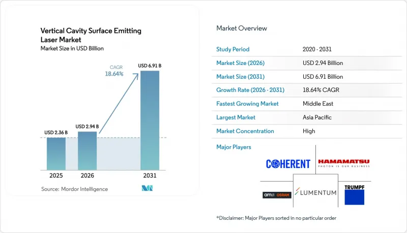
本報告依波長(紅光、近紅外線、短波紅外線)、晶片尺寸(0.02–0.06 mm²、0.06–0.4 mm²、0.4–1.3 mm²、1.0–7.5 mm²)、終端用戶產業(通訊、行動及消費性電子、汽車、醫療、工業、航太及防電區進行細分( SADAS)市場預測以美元計價。
全球垂直共振腔面射型雷射(VCSEL)市場趨勢及洞察
在人工智慧最佳化的超大規模資料中心中,基於VCSEL的光鏈路的應用正在迅速增加。
為了應對東西向流量,超大規模營運商正在將網路通道從 100 Gigabit升級到 200 Gigabit,因為東西向流量的成長速度是傳統雲端工作負載的 4.2 倍。目前,2D 64 發射器陣列每個模組的吞吐量可達 1.6 Terabit,與矽光電相比,每Gigabit的收發器成本降低了 18%,每Terabit的功耗降至 3.8 瓦。將 VCSEL 晶片整合到交換器 ASIC 上的共封裝光學模組正變得越來越普遍,它們取代了前面板模組,將跳頻延遲降低了 12 奈秒,並加速了短距離多模鏈路的普及。由於微軟 Azure 等服務供應商的目標是將電源使用效率 (PUE) 控制在 1.15 以下,VCSEL 的效率優勢正在推動垂直共振器面發射雷射 (VCSEL) 市場的成長。由津貼資金籌措的資本密集型晶圓廠正在確保本地供應穩定並加快產品認證週期。
將用於 3D 感測的 VCSEL 陣列快速整合到旗艦和中階智慧型手機中
智慧型手機製造商正在將940奈米泛光照明器整合到售價低於400美元的設備中,預計2024年至2027年間目標設備數量將翻倍。這款新型點陣投影機即使在陽光直射下也能在不到0.4秒的時間內完成臉部認證,同時保持超過1.2瓦的峰值輸出功率。其緊湊的2.4毫米 x 3.2毫米單晶片模組可將基板空間減少34%,方便在折疊式鉸鍊和穿戴式設備中應用。高品質的深度圖支援設備上的AR濾鏡和手勢導航功能,而與汽車座艙攝影機的跨產業大規模生產每年可降低0.14美元的晶圓成本。廣泛的應用場景正在推動垂直共振腔面射型雷射(VCSEL)市場實現兩位數成長,即使智慧型手機出貨量保持平穩。
基於 InP 的 VCSEL 外延的低良率限制了長波長產品的供應。
磷化銦 (InP) 晶圓的缺陷密度仍然是砷化鎵 (GaAs) 晶圓的 2.3 倍,這降低了良率,並使晶圓成本比 940 奈米同等製程高出 1.80 美元,這對價格敏感的消費性電子產品來說是一筆不小的負擔。雖然 3 吋晶圓基板的平均價格為 420 美元,但金屬有機化學氣相沉積 (MOCVD) 設備的運轉率僅為 68%,遠未達到規模經濟。一項 4,800 萬美元的擴建計畫預計要到 2027 年下半年才能全面投產,這可能會延長顯示整合感測器和長途資料通訊鏈路的供不應求。這套頸暫時阻礙了垂直共振器面發射雷射 (VCSEL) 市場的成長,而該市場原本預計將實現強勁成長。
細分市場分析
波長在750奈米至1400奈米範圍內的近紅外線裝置將在2025年佔據56.72%的銷售額,使其成為資料通訊通訊收發器和智慧型手機深度相機的核心細分市場。由於IEC 60825標準的放寬(允許光輸出提高10倍),波長在1400奈米至3000奈米範圍內的短波長紅外線發射器正以19.37%的複合年成長率快速成長。這對於需要在不發出視網膜損傷警告的情況下掃描超過1.2公尺範圍的車載監控系統而言,是一項重大變革。
根據 Lumentum 預測,到 2025 年,短波紅外線產品的出貨量預計將年增 34%,汽車行業的頂級供應商正在將 1550 奈米陣列整合到抬頭顯示器中。隨著光電滑鼠被電容式介面取代,波長低於 750 奈米的紅色雷射的需求持續下降。供應鏈正呈現兩極化:砷化鎵晶圓廠優先處理 850 奈米和 940 奈米陣列的大批量訂單,而磷化銦晶圓廠則在汽車和醫療領域追求更高的利潤率,所有這些都在重塑垂直共振器面發射雷射 (VCSEL) 市場。
預計到2025年,尺寸為0.06–0.4 mm²的雷射雷達將佔據39.14%的市場佔有率,該尺寸既能平衡智慧型手機的熱負荷,又能確保臉部辨識性能。而尺寸為1.0–7.5 mm²的雷射雷達則以19.61%的年成長率保持成長,以滿足200公尺雷射雷達所需的8 kW/cm²輻照度閾值。這一成長主要源自於對高性能雷射雷達系統的需求不斷成長,尤其是在自動駕駛汽車、機器人和先進測繪技術等需要精準高效感測的應用領域。
ams OSRAM 目前正在出貨用於中型乘用車的 3.5 mm² 多結陣列雷射器,其峰值輸出功率可達 100 瓦。 TRUMPF 的 7.2 mm² 晶片實現了 400 瓦的脈衝輸出功率,但佔空比僅為 0.8%,因此正在實施微通道冷卻方案。晶片面積越大,良率越低,從 88% 降至 72%(與中尺寸晶片相比),因此必須透過分析生產線來減少缺陷產品。這種規模的變化凸顯了高級駕駛輔助系統 (ADAS) 的普及如何重塑垂直共振腔面射型雷射(VCSEL) 市場的收入結構。
區域分析
預計到2025年,亞太地區將佔據全球半導體市場35.77%的主導地位。這主要得益於台灣和日本外延晶圓廠高達82%的運轉率。這一強勁表現,得益於製造能力的提升和對最尖端科技的旺盛需求,凸顯了該地區在全球半導體市場中的關鍵地位。同時,中國已向其化合物半導體基金投資280億元人民幣,戰略目標是2027年實現850奈米和940奈米技術的自主研發。這反映了中國致力於減少對進口的依賴,並加強國內半導體生態系統建設的決心。
在《晶片與資訊安全法案》(CHIPS Act)提供的18億美元津貼支持下,相干公司(Coherent)和Lumentum公司正在北美地區拓展業務。這項津貼旨在透過確保更穩定、更安全的供應鏈,幫助超大規模資料中心業者大規模資料中心降低供應風險。資金將用於支持對超大規模資料中心至關重要的先進光電技術的研發。同時,歐洲,尤其是德國光電帶,正受益於其位置一級汽車製造商的優勢。這不僅將VCSEL的前置作業時間從14週縮短至9週,也拓展了與主要汽車製造商的合作機會,加速了光電應用領域的創新。
主權財富基金對沙烏地阿拉伯和阿拉伯聯合大公國超大規模園區的投資正在增加,預計中東和非洲地區的複合年成長率將達到19.73%。這些投資旨在支持在地化、大規模語言模型的培養,這對於提升該地區的技術能力至關重要。此外,地理多元化在降低政治供應鏈風險方面發揮關鍵作用,從而增強全球垂直共振器面發射雷射(VCSEL)市場,並確保其抵禦地緣政治不確定性。
其他好處:
- Excel格式的市場預測(ME)表
- 3個月的分析師支持
目錄
第1章:引言
- 研究假設和市場定義
- 調查範圍
第2章:調查方法
第3章執行摘要
第4章 市場狀況
- 市場概覽
- 市場促進因素
- 在人工智慧最佳化的超大規模資料中心中,基於VCSEL的光鏈路的應用正在迅速增加。
- 旗艦級和中階智慧型手機快速採用3D感測VCSEL陣列
- 過渡到長波長(1.3µm)VCSEL 使得在顯示器下方實現生物識別模組成為可能。
- 支援高解析度固態雷射雷達的多結垂直腔面發射雷射器,適用於高級駕駛輔助系統 (ADAS)。
- GaN-on-Si VCSEL 平台正在降低每個發射器的成本,並擴大可見光市場。
- 政府主導的半導體產業回流激勵措施正在加速新建VCSEL製造工廠。
- 市場限制因素
- 基於 InP 的 VCSEL 外延生長良率低,限制了長波長產品的供應。
- 下一代資料中心架構中短距離光纖傳輸與矽光電的比較
- 智慧財產權的集中導致新興VCSEL供應商的授權成本不斷上升。
- 嚴格的眼部安全法規限制了車載應用的功率輸出。
- 產業價值鏈分析
- 監理情勢
- 技術展望
- 波特五力分析
- 宏觀經濟因素對市場的影響
- 專利整體情況
- 主要趨勢分析
第5章 市場規模與成長預測
- 波長
- 紅色(650-750 奈米)
- 近紅外線(750-1400奈米)
- 短波紅外線(1400-3000奈米)
- 按模具尺寸
- 0.02~0.06 mm2
- 0.06~0.4 mm2
- 0.4~1.3 mm2
- 1.0~7.5 mm2
- 按最終用戶行業分類
- 溝通
- 行動和消費者
- 車
- 醫學領域
- 產業
- 航太/國防
- 透過使用
- 資料通訊
- 臉部辨識與深度鏡頭
- 手勢姿態辨識
- 接近感應
- 雷射自動對焦
- 虹膜掃描
- 醫學診斷
- 用於高級駕駛輔助系統的雷射雷達
- 工業加工
- 光學滑鼠
- 其他用途
- 按地區
- 北美洲
- 美國
- 加拿大
- 墨西哥
- 歐洲
- 德國
- 英國
- 法國
- 俄羅斯
- 其他歐洲國家
- 亞太地區
- 中國
- 日本
- 印度
- 韓國
- 澳洲
- 其他亞太國家
- 中東和非洲
- 中東
- 沙烏地阿拉伯
- 阿拉伯聯合大公國
- 其他中東國家
- 非洲
- 南非
- 埃及
- 其他非洲國家
- 中東
- 南美洲
- 巴西
- 阿根廷
- 其他南美國家
- 北美洲
第6章 競爭情勢
- 市場集中度
- 策略趨勢
- 市佔率分析
- 公司簡介
- Coherent Corporation
- Lumentum Operations LLC
- ams OSRAM AG
- TRUMPF Group
- Broadcom Inc.
- Hamamatsu Photonics KK
- HLJ Technology Co. Ltd
- Teledyne FLIR Systems Inc.
- Vertilite Inc.
- Leonardo Electronics US
- Santec Corporation
- IQE plc
- WIN Semiconductors Corp.
- Bandwidth10 Inc.
- VERTILAS GmbH
- Ushio America Inc.
- Inneos LLC
- Frankfurt Laser Company
- Alight Technologies ApS
第7章 市場機會與未來展望
According to Mordor Intelligence, the vertical cavity surface-emitting laser market size was USD 2.94 billion in 2026 and is projected to reach USD 6.91 billion by 2031, growing at an 18.64% CAGR.
This report is Segmented by Wavelength (Red, Near-Infrared, Shortwave-Infrared), Die Size (0. 02-0. 06 Mm2, 0. 06-0. 4 Mm2, 0. 4-1. 3 Mm2, 1. 0-7. 5 Mm2), End-User Industry (Telecom, Mobile and Consumer, Automotive, Medical, Industrial, Aerospace and Defense), Application (Datacom, Iris Scan, ADAS LiDAR, and More), and Geography. The Market Forecasts are Provided in Terms of Value (USD).
Global Vertical Cavity Surface Emitting Laser Market Trends and Insights
Surging Adoption of VCSEL-Based Optical Links in AI-Optimized Hyperscale Data Centers
Hyperscale operators are upgrading from 100 gigabit to 200 gigabit lanes to satisfy east-west traffic that scales 4.2 times faster than traditional cloud workloads. Two-dimensional 64-emitter arrays now deliver 1.6 terabit throughput per module, reducing transceiver cost by 18% per gigabit and lowering power draw to 3.8 watts per terabit compared to silicon-photonics alternatives. Front-panel modules are giving way to co-packaged optics that seat VCSEL dies on switch ASICs, cutting hop latency by 12 nanoseconds and driving preference for short-reach multimode links. As Microsoft Azure and other providers strive to achieve power-usage-effectiveness ratios below 1.15, the efficiency advantage of VCSELs bolsters the vertical cavity surface-emitting laser market. Capital-intensive fabs funded by CHIPS Act grants ensure local supply security and accelerate product qualification cycles.
Rapid Integration of 3D Sensing VCSEL Arrays in Flagship and Mid-Tier Smartphones
Smartphone brands have pushed 940-nanometer flood illuminators into devices priced under USD 400, doubling the addressable unit base between 2024 and 2027. New dot projectors exceed 1.2 watts peak power yet unlock faces in under 0.4 seconds under bright sunlight. Compact 2.4 mm X 3.2 mm monolithic modules shave 34% board space, easing adoption in foldable hinges and wearables. Depth-map quality supports on-device AR filters and gesture navigation, while cross-industry volumes with automotive cabin cameras erode die cost by USD 0.14 annually. The use case breadth sustains double-digit growth for the vertical cavity surface-emitting laser market, even as overall smartphone shipments plateau.
Limited Yield for InP-Based VCSEL Epitaxy Constrains Long-Wave Supply
Defect densities in indium phosphide wafers remain 2.3 times higher than those in gallium arsenide, suppressing yield and keeping die costs USD 1.80 above those of 940-nanometer equivalents, a burden for price-sensitive consumer gadgets. Substrate prices average USD 420 for a 3-inch wafer, while metal-organic chemical vapor deposition reactors run at only 68% utilization, far from scale economies. Planned expansions worth USD 48 million will not reach full output until late 2027, prolonging shortages for under-display sensors and long-reach datacom links. The bottleneck temporarily hinders the otherwise robust growth of the vertical cavity surface-emitting laser market.
Other drivers and restraints analyzed in the detailed report include:
- Transition to Long-Wavelength 1.3 µm VCSELs Enabling Under-Display Biometric Modules
- Multi-Junction VCSELs Powering High-Resolution Solid-State LiDAR for ADAS
- Short Optical Reach Versus Silicon Photonics in Next-Generation Data Centers
For complete list of drivers and restraints, kindly check the Table Of Contents.
Segment Analysis
Near-infrared devices, ranging from 750 nanometers to 1,400 nanometers, controlled 56.72% of the revenue in 2025, an anchor segment for datacom transceivers and smartphone depth cameras. Shortwave-infrared emitters between 1,400 nanometers and 3,000 nanometers are expanding at a 19.37% CAGR due to looser IEC 60825 limits that allow 10 times higher optical power, a game-changer for cabin monitoring systems that must scan beyond 1.2 meters without triggering retinal-hazard warnings.
Lumentum documented 34% year-over-year growth in shortwave-infrared shipments in 2025, with automotive tier-1 suppliers integrating 1,550-nanometer arrays into head-up displays. Red wavelengths below 750 nanometers continue to fade as optical mice give way to capacitive interfaces. Bifurcated supply chains emerge: gallium arsenide fabs prioritize high-volume orders for 850 nanometer and 940 nanometer, while indium phosphide specialists chase automotive and medical margins, collectively reshaping the vertical cavity surface-emitting laser market.
The footprints of 0.06-0.4 mm2 held a 39.14% share in 2025, as they balance thermal load with facial-recognition performance inside smartphones. To meet the 8 kW/cm2 irradiance threshold required for a 200-meter LiDAR, formats ranging from 1.0 to 7.5 mm2 are witnessing an impressive annual growth rate of 19.61%. This growth is driven by the increasing demand for high-performance LiDAR systems in applications such as autonomous vehicles, robotics, and advanced mapping technologies, where precise and efficient sensing capabilities are critical.
ams OSRAM now ships 3.5 mm2 multi-junction arrays that reach 100-watt peaks for mid-range passenger cars. TRUMPF's 7.2 mm2 dies demonstrated 400-watt bursts, although limited to 0.8% duty cycles, prompting the implementation of microchannel cooling programs. Larger die areas yield 72% versus 88% for mid-sizes, prompting fabrication-line analytics to mitigate scrap. The scale shift highlights how ADAS adoption reconfigures revenue pools within the vertical cavity surface-emitting laser market.
Complete Report Scope:
- By Wavelength
- Red (650-750 nm)
- Near-Infrared (750-1400 nm)
- Shortwave-Infrared (1400-3000 nm)
- By Die Size
- 0.02 - 0.06 mm2
- 0.06 - 0.4 mm2
- 0.4 - 1.3 mm2
- 1.0 - 7.5 mm2
- By End-User Industry
- Telecom
- Mobile and Consumer
- Automotive
- Medical
- Industrial
- Aerospace and Defense
- By Application
- Datacom
- Facial Recognition and Depth Camera
- Gesture Recognition
- Proximity Sensing
- Laser Autofocus
- Iris Scan
- Medical Diagnostics
- ADAS LiDAR
- Industrial Processing
- Optical Mouse
- Other Application
- By Geography
- North America
- United States
- Canada
- Mexico
- Europe
- Germany
- United Kingdom
- France
- Russia
- Rest of Europe
- Asia-Pacific
- China
- Japan
- India
- South Korea
- Australia
- Rest of Asia-Pacific
- Middle East and Africa
- Middle East
- Saudi Arabia
- United Arab Emirates
- Rest of Middle East
- Africa
- South Africa
- Egypt
- Rest of Africa
- Middle East
- South America
- Brazil
- Argentina
- Rest of South America
- North America
Geography Analysis
In 2025, the Asia-Pacific region commanded a dominant 35.77% share, buoyed by Taiwanese and Japanese epitaxial fabs running at an impressive 82% utilization rate. This strong performance highlights the region's pivotal role in the global semiconductor market, driven by advancements in manufacturing capabilities and robust demand for cutting-edge technologies. Meanwhile, China's CNY 28 billion investment in its compound semiconductor fund is strategically targeting self-sufficiency in 850-nanometer and 940-nanometer technologies by 2027, reflecting the country's commitment to reducing reliance on imports and strengthening its domestic semiconductor ecosystem.
Coherent and Lumentum have expanded in North America, bolstered by USD 1.8 billion in CHIPS Act grants, which mitigate supply risks for hyperscalers by ensuring a more stable and secure supply chain. This funding supports the development of advanced photonics technologies critical for hyperscale data centers. Meanwhile, Europe, centered in Germany's photonics belt, benefits from its closeness to automotive tier-1 plants, which not only reduces VCSEL lead times from 14 weeks to just 9 but also enhances collaboration opportunities with key automotive manufacturers, fostering innovation in photonics applications.
Sovereign funds are increasingly investing in hyperscale campuses in Saudi Arabia and the UAE, driving a projected 19.73% CAGR in the Middle East and Africa. These investments aim to support the training of localized large-language models, which are critical for advancing regional technological capabilities. Additionally, geographic diversification is playing a key role in mitigating political supply chain risks, thereby strengthening the global vertical cavity surface-emitting laser market and ensuring its resilience against geopolitical uncertainties.
- Coherent Corporation
- Lumentum Operations LLC
- ams OSRAM AG
- TRUMPF Group
- Broadcom Inc.
- Hamamatsu Photonics KK
- HLJ Technology Co. Ltd
- Teledyne FLIR Systems Inc.
- Vertilite Inc.
- Leonardo Electronics US
- Santec Corporation
- IQE plc
- WIN Semiconductors Corp.
- Bandwidth10 Inc.
- VERTILAS GmbH
- Ushio America Inc.
- Inneos LLC
- Frankfurt Laser Company
- Alight Technologies ApS
Additional Benefits:
- The market estimate (ME) sheet in Excel format
- 3 months of analyst support
TABLE OF CONTENTS
1 INTRODUCTION
- 1.1 Study Assumptions and Market Definition
- 1.2 Scope of the Study
2 RESEARCH METHODOLOGY
3 EXECUTIVE SUMMARY
4 MARKET LANDSCAPE
- 4.1 Market Overview
- 4.2 Market Drivers
- 4.2.1 Surging Adoption of VCSEL-Based Optical Links in AI-Optimized Hyperscale Data Centers
- 4.2.2 Rapid Integration of 3D Sensing VCSEL Arrays in Flagship and Mid-Tier Smartphones
- 4.2.3 Transition to Long-Wavelength (1.3 µm) VCSELs Enabling Under-Display Biometric Modules
- 4.2.4 Multi-Junction VCSELs Powering High-Resolution Solid-State LiDAR for ADAS
- 4.2.5 GaN-on-Si VCSEL Platforms Lowering Cost per Emitter and Expanding Visible-Light Markets
- 4.2.6 Government-Backed Semiconductor Reshoring Incentives Accelerating New VCSEL Fabs
- 4.3 Market Restraints
- 4.3.1 Limited Yield for InP-Based VCSEL Epitaxy Constrains Long-Wave Supply
- 4.3.2 Short Optical Reach Versus Silicon Photonics in Next-Gen Data-Center Architectures
- 4.3.3 IP Concentration Raises Licensing Costs for Emerging VCSEL Suppliers
- 4.3.4 Tight Eye-Safety Regulations Cap Output Power in Automotive Cabin Applications
- 4.4 Industry Value Chain Analysis
- 4.5 Regulatory Landscape
- 4.6 Technological Outlook
- 4.7 Porter's Five Forces Analysis
- 4.7.1 Bargaining Power of Suppliers
- 4.7.2 Bargaining Power of Buyers
- 4.7.3 Threat of New Entrants
- 4.7.4 Threat of Substitutes
- 4.7.5 Intensity of Competitive Rivalry
- 4.8 Impact of Macroeconomic Factors on the Market
- 4.9 Patent Landscape
- 4.10 Material Trend Analysis
5 MARKET SIZE AND GROWTH FORECASTS (VALUE)
- 5.1 By Wavelength
- 5.1.1 Red (650-750 nm)
- 5.1.2 Near-Infrared (750-1400 nm)
- 5.1.3 Shortwave-Infrared (1400-3000 nm)
- 5.2 By Die Size
- 5.2.1 0.02 - 0.06 mm2
- 5.2.2 0.06 - 0.4 mm2
- 5.2.3 0.4 - 1.3 mm2
- 5.2.4 1.0 - 7.5 mm2
- 5.3 By End-User Industry
- 5.3.1 Telecom
- 5.3.2 Mobile and Consumer
- 5.3.3 Automotive
- 5.3.4 Medical
- 5.3.5 Industrial
- 5.3.6 Aerospace and Defense
- 5.4 By Application
- 5.4.1 Datacom
- 5.4.2 Facial Recognition and Depth Camera
- 5.4.3 Gesture Recognition
- 5.4.4 Proximity Sensing
- 5.4.5 Laser Autofocus
- 5.4.6 Iris Scan
- 5.4.7 Medical Diagnostics
- 5.4.8 ADAS LiDAR
- 5.4.9 Industrial Processing
- 5.4.10 Optical Mouse
- 5.4.11 Other Application
- 5.5 By Geography
- 5.5.1 North America
- 5.5.1.1 United States
- 5.5.1.2 Canada
- 5.5.1.3 Mexico
- 5.5.2 Europe
- 5.5.2.1 Germany
- 5.5.2.2 United Kingdom
- 5.5.2.3 France
- 5.5.2.4 Russia
- 5.5.2.5 Rest of Europe
- 5.5.3 Asia-Pacific
- 5.5.3.1 China
- 5.5.3.2 Japan
- 5.5.3.3 India
- 5.5.3.4 South Korea
- 5.5.3.5 Australia
- 5.5.3.6 Rest of Asia-Pacific
- 5.5.4 Middle East and Africa
- 5.5.4.1 Middle East
- 5.5.4.1.1 Saudi Arabia
- 5.5.4.1.2 United Arab Emirates
- 5.5.4.1.3 Rest of Middle East
- 5.5.4.2 Africa
- 5.5.4.2.1 South Africa
- 5.5.4.2.2 Egypt
- 5.5.4.2.3 Rest of Africa
- 5.5.4.1 Middle East
- 5.5.5 South America
- 5.5.5.1 Brazil
- 5.5.5.2 Argentina
- 5.5.5.3 Rest of South America
- 5.5.1 North America
6 COMPETITIVE LANDSCAPE
- 6.1 Market Concentration
- 6.2 Strategic Moves
- 6.3 Market Share Analysis
- 6.4 Company Profiles (includes Global Level Overview, Market Level Overview, Core Segments, Financials as available, Strategic Information, Market Rank/Share for Key Companies, Products and Services, and Recent Developments)
- 6.4.1 Coherent Corporation
- 6.4.2 Lumentum Operations LLC
- 6.4.3 ams OSRAM AG
- 6.4.4 TRUMPF Group
- 6.4.5 Broadcom Inc.
- 6.4.6 Hamamatsu Photonics KK
- 6.4.7 HLJ Technology Co. Ltd
- 6.4.8 Teledyne FLIR Systems Inc.
- 6.4.9 Vertilite Inc.
- 6.4.10 Leonardo Electronics US
- 6.4.11 Santec Corporation
- 6.4.12 IQE plc
- 6.4.13 WIN Semiconductors Corp.
- 6.4.14 Bandwidth10 Inc.
- 6.4.15 VERTILAS GmbH
- 6.4.16 Ushio America Inc.
- 6.4.17 Inneos LLC
- 6.4.18 Frankfurt Laser Company
- 6.4.19 Alight Technologies ApS
7 MARKET OPPORTUNITIES AND FUTURE OUTLOOK
- 7.1 White-Space and Unmet-Need Assessment

 全球VCSEL市場:按類型、波長、材料、數據速率、光輸出、產業和地區分類-預測至2032年
 航空電子和無線設備測試市場報告:趨勢、預測和競爭分析(至2035年)
 垂直共振腔面射型雷射市場-2026-2032年全球市場預測
 VCSEL全球市場規模、佔有率、趨勢和成長分析報告:2026-2034年
 垂直共振腔面射型雷射市場報告:按類型、材料、波長、應用、終端用戶產業和地區分類(2026-2034 年)
 VCSEL雷射器市場規模、佔有率和成長分析:按產品類型、應用、最終用戶、波長和地區分類-2026-2033年產業預測
 覆晶VCSEL市場規模、佔有率和成長分析:按元件類型、應用、材料類型、終端用戶產業和地區分類-2026-2033年產業預測
 VCSEL市場分析及至2035年預測:依類型、產品、應用、技術、材料類型、組件、最終用戶、製程、功能及安裝類型分類全球光子晶體表面發光二極體市場規模、佔有率、趨勢和成長分析報告(2026-2034)
 2026年全球垂直共振腔面射型雷射(VCSEL)市場報告