


 |
市場調查報告書
商品編碼
2122310
阻變式隨機存取記憶體:市場佔有率分析、產業趨勢與統計資料、成長預測(2026-2031)Resistive RAM - Market Share Analysis, Industry Trends & Statistics, Growth Forecasts (2026 - 2031) |
||||||

※ 本網頁內容可能與最新版本有所差異。詳細情況請與我們聯繫。
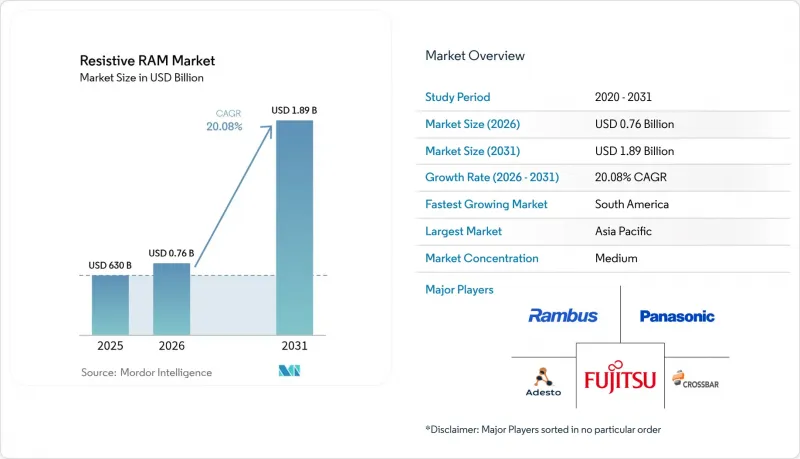
據 Mordor Intelligence 稱,電阻式隨機存取記憶體 (ReRAM) 的市場規模預計在 2026 年達到 7.565 億美元,高於 2025 年的 6.3 億美元,預計到 2031 年將達到 18.9 億美元。
預計 2026 年至 2031 年的複合年成長率為 20.08%。
本報告按材料類型(氧化物基、導電橋、奈米金屬絲)、外形規格(嵌入式 ReRAM、獨立式 ReRAM)、應用(記憶體內運算、持久存儲、高速啟動代碼存儲)、最終用戶(工業/物聯網設備、汽車/移動出行、其他)和地區(北美、南美、歐洲、亞太、中東和非洲)進行分類。
全球電阻式隨機存取記憶體(RRAM)市場趨勢及洞察
突破性的耐用性,超過 1012 次循環。
由於其耐久性超過 10¹² 次循環,ReRAM 已成為寫入密集型企業工作負載中快閃記憶體的可行替代方案。一個研究團隊報告了一種鋁氮化鐵電堆疊結構,該結構在保持極化狀態的同時,能夠承受 10¹°C 的循環。隨後,Weebit Nano 在汽車測試中檢驗了在 150 度C下 10 萬次編程循環的性能。這種耐久性使得儲存廠商開始考慮將 ReRAM 用於傳統上以 DRAM 為標準的熱層快取。
低於 1V 的開關特性可實現超低功耗的邊緣元件。
維吉尼亞大學的一項研究表明,0.6V 導電橋 ReRAM 宏模組每次寫入週期消耗 8 pJ 的能量,無需電荷泵。英特爾也在 22FFL 節點上展示了基於 FinFET 的嵌入式 ReRAM,證實了在低於 1V 電壓下運作的可行性。提高電池續航時間是包括穿戴式裝置、感測器節點和智慧電錶在內的眾多領域都至關重要的問題。
由於耗材變化引起的寫入雜訊和位元錯誤。
導電通道的偏差降低了高可靠性生產的良率。對Ta2O5裝置的研究表明,電壓相關雜訊與神經陣列中權重解析度的降低有關。交叉陣列尺度的熱相互作用也增加了不確定性。 Al2O3疊層中的喚醒增值回收是一種緩解措施,但它導致製程延長。
細分市場分析
到2025年,氧化物基元件仍將佔據電阻式隨機存取記憶體(RRAM)市場45.85%的佔有率。 HfO2和Al2O3疊層結構已整合到主流CMOS製程中,降低了部署風險。導電橋型(主要基於銅)的複合年成長率(CAGR)預計為25.45%,其低於1V的寫入能力滿足了穿戴式裝置和微功耗節點的需求。預計到2031年,導電橋型RRAM的市場規模將達到6億美元,反映出設計人員對邊緣架構能源效率裕度的重視。奈米金屬絲製程滿足了對極緻小型化和高抗輻射性能的特定需求。混合碳纖維絲在37nm製程下實現了無模封裝,並展現出超過10⁷次循環的耐久性。
為了應對這項挑戰,氧化物基供應商採用空位控制層來降低循環間變異性並提高耐久性。如今,代工廠庫已將氧化物基 ReRAM 巨集與邏輯 IP 捆綁在一起,簡化了 MCU 流片流程。同時,導電橋架構的支持者則強調了其更低的程式電流和更長的電池壽命等優勢。雙方都投資進行了用於神經網路的模擬權重儲存的概念驗證實驗,以推動人工智慧加速器市場的發展。
到2025年,嵌入式解決方案將佔銷售額的54.85%,因為系統晶片(SoC) 設計人員優先考慮的是晶片面積的節省和材料清單(BOM) 的簡化。 MCU 供應商整合了1-4 Mbit的宏,用於安全代碼存儲、韌體更新和即時啟動功能。儘管獨立儲存密度有所提高,但預計到2031年,電阻式隨機存取記憶體 (RRAM) 在嵌入式裝置中的市佔率仍將維持在50%以上。
隨著人工智慧和高效能運算 (HPC) 客戶對客製化記憶體模組的需求不斷成長,獨立式 ReRAM 的複合年成長率預計將達到 24.6%。設計人員現在可以在不受邏輯約束的情況下調整陣列幾何結構和選擇器堆疊,從而實現更大的字線,以進行並行模擬乘法和積分運算。一個 4 Mbit 的「記憶體內運算」宏,具有 8 位元精度,能夠以微焦耳級的功耗進行推理處理。雲端供應商已將這些獨立晶片評估為可與 DRAM 快取配合使用的裝置,用於那些受益於原位權重更新的訓練工作負載。
區域分析
到2025年,亞太地區將佔全球銷售額的40.85%。三星、SK海力士和鎧俠等公司的大規模晶圓代工投資擴大了28nm以下嵌入式ReRAM設計套件的市場。韓國撥款750億美元,計畫在2028年擴大先進記憶體產能,投資高頻寬和下一代非揮發性記憶體(NVM)產品線。日本則推行了一項670億美元的半導體振興計劃,將ReRAM應用於人工智慧邊緣裝置。
南美洲成為成長最快的地區,複合年成長率高達21.65%。巴西投資6.5億雷亞爾(約1.3億美元)用於擴建,旨在阿提巴希亞和馬瑙斯實現封裝和檢測流程的本地化,從而實現ReRAM和DRAM的封裝。該地區政府也致力於促進用於氧化膜的稀土元素礦物供應。因此,南美洲的電阻式隨機存取記憶體(RRAM)市場受益於垂直整合的激勵措施。北美憑藉著在汽車和航太領域(這些領域對抗輻射性能有要求)的應用案例,保持了其設計主導。隨著高級駕駛輔助系統(ADAS)記憶體配置的變化,預計美國和加拿大的RRAM市場規模將進一步擴大。在歐洲,重點是工業控制供應商整合用於即時分析的「記憶體計算」(CI-M)宏。在中東和非洲,由於低功耗持久性記憶體縮短了智慧城市感測器網路的維護週期,市場需求早期就已開始成長。
其他好處
- Excel格式的市場預測(ME)表
- 3個月的分析師支持
目錄
第1章:引言
- 研究假設和市場定義
- 調查範圍
第2章:調查方法
第3章執行摘要
第4章 市場狀況
- 市場概覽
- 市場促進因素
- 突破性的耐用性,超過 1012 次循環。
- 低於 1V 的開關特性可實現超低功耗的邊緣元件。
- 28nm及以下製程的嵌入式ReRAM代工廠支持
- 汽車高級駕駛輔助系統(ADAS)對耐高溫非揮發性記憶體(NVM)的需求日益成長。
- 神經形態計算領域新創企業的資金籌措激增
- 市場限制因素
- 由於耗材變化引起的寫入雜訊和位元錯誤。
- 除了極少數授權者之外,其他地區缺乏智慧財產權和技術訣竅。
- 與 3D NAND BEOL 堆疊整合面臨的挑戰
- 宏觀經濟因素的影響
- 價值鏈分析
- 監理情勢
- 技術展望
- 波特五力分析
第5章 市場規模與成長預測
- 依材料類型
- 基於氧化物的(OxRRAM)
- 導電橋(CBRAM)
- 奈米金屬絲
- 按外形規格
- 嵌入式 ReRAM
- 獨立式 ReRAM
- 透過使用
- 記憶體內運算
- 持久性儲存
- 高速引導碼存儲
- 最終用戶
- 工業和物聯網設備
- 汽車與出行
- 資料中心與企業的固態硬碟
- 穿戴式裝置和家用電子設備
- 按地區
- 北美洲
- 美國
- 加拿大
- 南美洲
- 巴西
- 其他南美國家
- 歐洲
- 德國
- 法國
- 英國
- 義大利
- 西班牙
- 俄羅斯
- 其他歐洲國家
- 亞太地區
- 中國
- 日本
- 韓國
- 台灣
- 印度
- 其他亞太國家
- 中東和非洲
- 中東
- 沙烏地阿拉伯
- 阿拉伯聯合大公國
- 土耳其
- 其他中東國家
- 非洲
- 南非
- 奈及利亞
- 其他非洲地區
- 中東
- 北美洲
第6章 競爭情勢
- 市場集中度
- 策略趨勢
- 市佔率分析
- 公司簡介
- Crossbar Inc.
- Weebit Nano Ltd.
- 4DS Memory Limited
- Fujitsu Semiconductor Memory Solution Ltd.
- Xinyuan Semiconductor(Shanghai)Co., Ltd.
- Dialog Semiconductor Ltd.(Renesas)
- Panasonic Holdings Corp.
- Sony Semiconductor Solutions Corp.
- Micron Technology Inc.
- Intel Corporation
- IBM Corporation
- Western Digital Technologies, Inc.
- SK hynix Inc.
- Samsung Electronics Co., Ltd.
- TDK Corporation
- Infineon Technologies AG
- Renesas Electronics Corp.
- SMIC
- TetraMem Inc.
- ReRam Nanotech Ltd.
- Adesto Technologies Corp.(Dialog)
- Avalanche Technology Inc.
- RRAMTech Srl
- CEA-Leti
- GigaDevice Semiconductor Inc.
第7章 市場機會與未來展望
According to Mordor Intelligence, resistive random access memory market size in 2026 is estimated at USD 756.5 million, growing from 2025 value of USD 630 million with 2031 projections showing USD 1.89 billion, growing at 20.08% CAGR over 2026-2031.
This report is Segmented by Material Type (Oxide-Based, Conductive-Bridge, and Nanometal Filament), Form Factor (Embedded ReRAM, and Stand-Alone ReRAM), Application (In-Memory Computing, Persistent Storage, and Fast Boot/Code Storage), End-User (Industrial and IoT Devices, Automotive and Mobility, and More), and Geography (North America, South America, Europe, Asia-Pacific, and Middle East and Africa).
Global Resistive RAM Market Trends and Insights
Breakthrough endurance beyond 1012 cycles
Endurance exceeding 1012 cycles positioned ReRAM as a realistic flash replacement for write-intensive enterprise workloads. Academic teams reported aluminum-scandium nitride ferroelectric stacks persisting through 101° cycles while retaining polarization.Weebit Nano later validated 100,000 program cycles at 150 °C during automotive tests. This durability lets storage vendors contemplate using ReRAM for hot-tier caching that had previously defaulted to DRAM.
Sub-1 V switching for ultra-low-power edge devices
Research from the University of Virginia showed a 0.6 V conductive-bridge ReRAM macro consuming 8 pJ per write, eliminating charge-pump overhead. Intel echoed the feasibility of sub-1V operation when it demonstrated FinFET-based embedded ReRAM on 22FFL nodes. Battery life gains mattered across wearables, sensor nodes, and smart meters.
Filament variability causing write-noise and bit-error
Variability in conductive paths hampered yield during high-reliability production. Studies on Ta2O5 devices linked voltage-dependent noise to degraded weight resolution in neural arrays. Crossbar-scale thermal interactions added uncertainty. Wake-up cycling in Al2O3 stacks offered mitigation but lengthened process flows.
Other drivers and restraints analyzed in the detailed report include:
- Foundry support for embedded ReRAM at 28 nm and below
- Automotive ADAS demand for high-temperature NVM
- Limited IP and know-how outside a few licensors
For complete list of drivers and restraints, kindly check the Table Of Contents.
Segment Analysis
Oxide-based devices retained 45.85% share of the resistive random access memory market in 2025. HfO2 and Al2O3 stacks were already part of mainstream CMOS flows, which lowered adoption risk. Conductive-bridge variants, often copper-based, registered a 25.45% CAGR outlook because their sub-1V write capability aligned with wearables and micro-power nodes. The resistive random access memory market size for conductive-bridge devices is projected to reach USD 0.60 billion by 2031, reflecting designers' preference for energy headroom in edge architectures. Nanometal filament approaches captured niche demand where extreme miniaturization or high radiation tolerance mattered. Hybrid carbon filaments demonstrated forming-free operation at 37 nm with >107 cycles.
Oxide-based suppliers responded by enhancing endurance through vacancy-engineered layers that reduced cycle-to-cycle variability. Foundry libraries now bundle oxide-based ReRAM macros alongside logic IP, simplifying MCU tape-outs. Conversely, conductive-bridge proponents leveraged lower programming currents to market battery-life gains. Both camps invested in neural-network analog weight storage demonstrations to tap AI accelerators.
Embedded solutions held 54.85% of revenue in 2025 because system-on-chip designers valued die-space savings and simplified bills of materials. MCU vendors embedded 1-4 Mbit macros for secure code storage, firmware updates, and instant-on features. The resistive random access memory market share of embedded devices is expected to remain above 50% through 2031, even as stand-alone density rises.
Stand-alone ReRAM recorded a 24.6% CAGR projection as AI and HPC customers sought bespoke memory modules. Designers could tune array geometry and selector stacks without logic constraints, enabling larger word lines for parallel analog multiply-accumulate. A 4 Mbit compute-in-memory macro with 8-bit precision demonstrated inference at micro-joule energy levels. Cloud vendors evaluated these stand-alone chips as DRAM cache complements for training workloads that benefit from in-situ weight updates.
Complete Report Scope:
- By Material Type
- Oxide-based (OxRRAM)
- Conductive-Bridge (CBRAM)
- Nanometal Filament
- By Form Factor
- Embedded ReRAM
- Stand-alone ReRAM
- By Application
- In-Memory Computing
- Persistent Storage
- Fast Boot / Code Storage
- By End-user
- Industrial and IoT Devices
- Automotive and Mobility
- Datacentres and Enterprise SSD
- Wearables and Consumer Electronics
- By Geography
- North America
- United States
- Canada
- South America
- Brazil
- Rest of South America
- Europe
- Germany
- France
- United Kingdom
- Italy
- Spain
- Russia
- Rest of Europe
- Asia-Pacific
- China
- Japan
- South Korea
- Taiwan
- India
- Rest of Asia-Pacific
- Middle East and Africa
- Middle East
- Saudi Arabia
- United Arab Emirates
- Turkey
- Rest of Middle East
- Africa
- South Africa
- Nigeria
- Rest of Africa
- Middle East
- North America
Geography Analysis
Asia-Pacific commanded 40.85% revenue in 2025. Massive foundry investments by Samsung, SK Hynix, and Kioxia expanded embedded ReRAM design kits below 28 nm. South Korea allocated USD 75 billion for advanced memory capacity through 2028, funneling funds into high-bandwidth and next-generation NVM lines. Japan pursued a USD 67 billion semiconductor renaissance plan with ReRAM earmarked for AI edge devices.
South America emerged as the fastest-growing cluster, posting 21.65% CAGR. Brazil funded a R$650 million (USD 130 million) expansion in Atibaia and Manaus to localize encapsulation and test, targeting both ReRAM and DRAM packaging. Regional governments also facilitated the rare-earth mineral supply for oxide films. The resistive random access memory market in South America, therefore, benefited from vertical integration incentives. North America retained design leadership, leveraging automotive and aerospace use cases that demand radiation hardening. The resistive random access memory market size for the US and Canada is forecast to climb alongside ADAS memory mix shifts. Europe focused on industrial control vendors integrating compute-in-memory macros for real-time analytics. The Middle East and Africa saw early traction in smart-city sensor grids where low-power persistent memory reduced maintenance cycles.
- Crossbar Inc.
- Weebit Nano Ltd.
- 4DS Memory Limited
- Fujitsu Semiconductor Memory Solution Ltd.
- Xinyuan Semiconductor (Shanghai) Co., Ltd.
- Dialog Semiconductor Ltd. (Renesas)
- Panasonic Holdings Corp.
- Sony Semiconductor Solutions Corp.
- Micron Technology Inc.
- Intel Corporation
- IBM Corporation
- Western Digital Technologies, Inc.
- SK hynix Inc.
- Samsung Electronics Co., Ltd.
- TDK Corporation
- Infineon Technologies AG
- Renesas Electronics Corp.
- SMIC
- TetraMem Inc.
- ReRam Nanotech Ltd.
- Adesto Technologies Corp. (Dialog)
- Avalanche Technology Inc.
- RRAMTech S.r.l.
- CEA-Leti
- GigaDevice Semiconductor Inc.
Additional Benefits:
- The market estimate (ME) sheet in Excel format
- 3 months of analyst support
TABLE OF CONTENTS
1 INTRODUCTION
- 1.1 Study Assumptions and Market Definition
- 1.2 Scope of the Study
2 RESEARCH METHODOLOGY
3 EXECUTIVE SUMMARY
4 MARKET LANDSCAPE
- 4.1 Market Overview
- 4.2 Market Drivers
- 4.2.1 Break-through endurance improvements beyond 1012 cycles
- 4.2.2 Sub-1 V switching enabling ultra-low-power edge devices
- 4.2.3 Foundry support for embedded ReRAM at 28 nm and below
- 4.2.4 Automotive ADAS demand for high-temperature NVM
- 4.2.5 VC funding surge in neuromorphic compute start-ups
- 4.3 Market Restraints
- 4.3.1 Filament variability causing write-noise and bit-error
- 4.3.2 Limited IP/know-how outside a handful of licensors
- 4.3.3 Challenging integration with 3D NAND BEOL stacks
- 4.4 Impact of Macroeconomic Factors
- 4.5 Value Chain Analysis
- 4.6 Regulatory Landscape
- 4.7 Technological Outlook
- 4.8 Porter's Five Forces Analysis
- 4.8.1 Bargaining Power of Suppliers
- 4.8.2 Bargaining Power of Buyers
- 4.8.3 Threat of New Entrants
- 4.8.4 Threat of Substitutes
- 4.8.5 Competitive Rivalry
5 MARKET SIZE AND GROWTH FORECASTS (VALUE)
- 5.1 By Material Type
- 5.1.1 Oxide-based (OxRRAM)
- 5.1.2 Conductive-Bridge (CBRAM)
- 5.1.3 Nanometal Filament
- 5.2 By Form Factor
- 5.2.1 Embedded ReRAM
- 5.2.2 Stand-alone ReRAM
- 5.3 By Application
- 5.3.1 In-Memory Computing
- 5.3.2 Persistent Storage
- 5.3.3 Fast Boot / Code Storage
- 5.4 By End-user
- 5.4.1 Industrial and IoT Devices
- 5.4.2 Automotive and Mobility
- 5.4.3 Datacentres and Enterprise SSD
- 5.4.4 Wearables and Consumer Electronics
- 5.5 By Geography
- 5.5.1 North America
- 5.5.1.1 United States
- 5.5.1.2 Canada
- 5.5.2 South America
- 5.5.2.1 Brazil
- 5.5.2.2 Rest of South America
- 5.5.3 Europe
- 5.5.3.1 Germany
- 5.5.3.2 France
- 5.5.3.3 United Kingdom
- 5.5.3.4 Italy
- 5.5.3.5 Spain
- 5.5.3.6 Russia
- 5.5.3.7 Rest of Europe
- 5.5.4 Asia-Pacific
- 5.5.4.1 China
- 5.5.4.2 Japan
- 5.5.4.3 South Korea
- 5.5.4.4 Taiwan
- 5.5.4.5 India
- 5.5.4.6 Rest of Asia-Pacific
- 5.5.5 Middle East and Africa
- 5.5.5.1 Middle East
- 5.5.5.1.1 Saudi Arabia
- 5.5.5.1.2 United Arab Emirates
- 5.5.5.1.3 Turkey
- 5.5.5.1.4 Rest of Middle East
- 5.5.5.2 Africa
- 5.5.5.2.1 South Africa
- 5.5.5.2.2 Nigeria
- 5.5.5.2.3 Rest of Africa
- 5.5.5.1 Middle East
- 5.5.1 North America
6 COMPETITIVE LANDSCAPE
- 6.1 Market Concentration
- 6.2 Strategic Moves
- 6.3 Market Share Analysis
- 6.4 Company Profiles (includes Global level Overview, Market level overview, Core Segments, Financials as available, Strategic Information, Market Rank/Share for key companies, Products and Services, and Recent Developments)
- 6.4.1 Crossbar Inc.
- 6.4.2 Weebit Nano Ltd.
- 6.4.3 4DS Memory Limited
- 6.4.4 Fujitsu Semiconductor Memory Solution Ltd.
- 6.4.5 Xinyuan Semiconductor (Shanghai) Co., Ltd.
- 6.4.6 Dialog Semiconductor Ltd. (Renesas)
- 6.4.7 Panasonic Holdings Corp.
- 6.4.8 Sony Semiconductor Solutions Corp.
- 6.4.9 Micron Technology Inc.
- 6.4.10 Intel Corporation
- 6.4.11 IBM Corporation
- 6.4.12 Western Digital Technologies, Inc.
- 6.4.13 SK hynix Inc.
- 6.4.14 Samsung Electronics Co., Ltd.
- 6.4.15 TDK Corporation
- 6.4.16 Infineon Technologies AG
- 6.4.17 Renesas Electronics Corp.
- 6.4.18 SMIC
- 6.4.19 TetraMem Inc.
- 6.4.20 ReRam Nanotech Ltd.
- 6.4.21 Adesto Technologies Corp. (Dialog)
- 6.4.22 Avalanche Technology Inc.
- 6.4.23 RRAMTech S.r.l.
- 6.4.24 CEA-Leti
- 6.4.25 GigaDevice Semiconductor Inc.
7 MARKET OPPORTUNITIES AND FUTURE OUTLOOK
- 7.1 White-space and Unmet-need Assessment

