


 |
市場調查報告書
商品編碼
2119581
探針卡:市場佔有率分析、產業趨勢與統計、成長預測(2026-2031)Probe Card - Market Share Analysis, Industry Trends & Statistics, Growth Forecasts (2026 - 2031) |
||||||

※ 本網頁內容可能與最新版本有所差異。詳細情況請與我們聯繫。
根據 Mordor Intelligence 預測,探針卡市場預計將從 2025 年的 27.2 億美元成長到 2026 年的 30.4 億美元,到 2031 年達到 47.5 億美元,2026 年至 2031 年的複合年成長率預計為 9.35%。
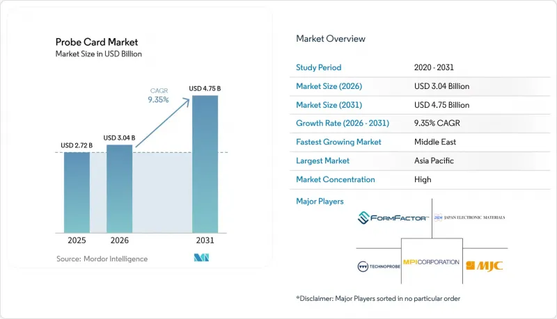
本報告按技術(MEMS、垂直結構、懸臂梁結構、特種結構)、應用(DRAM、快閃記憶體、代工和邏輯電路、參數化、其他)、類型(標準探針卡、高級探針卡)、最終用戶(代工廠、整合設備製造商、OSAT、研究機構)、晶圓尺寸(150mm、2004mm、30mmmm、2004mm)。市場預測以美元(USD)為單位。
全球探針卡市場趨勢及洞察
對家用電子電器和物聯網設備的需求不斷成長
預計到2025年,智慧型手機出貨量將趨於穩定在12億部,但受專用人工智慧引擎和先進電源管理積體電路的推動,每台設備的半導體數量將增加18%。屆時,汽車電子產品支出將達到820億美元,電動車每輛車最多可整合3,000個晶片。物聯網部署數量將超過160億,工業和醫療終端需要在極端溫度條件下進行混合訊號檢驗。這些變化意味著探針卡的需求不再僅由產量驅動,即使消費性產品產量趨於穩定,晶圓級測試領域仍將蓬勃發展。蘋果公司於2025年發布的客製化M4處理器進一步凸顯了其垂直整合策略,其整合記憶體架構需要客製化的探針解決方案。
半導體裝置的小型化
台積電將於2025年下半年開始量產其2nm環柵(GAA)工藝,這需要探針晶片能夠將自身定位精度控制在10微米以內,同時避免焊盤損傷。英特爾即將推出的18A節點將採用背面供電,需要雙面探針測試,而傳統的懸臂式探針卡無法勝任。三星的1.4nm藍圖顯示,探針更換頻率將比5nm製程翻倍,這將增加每片晶圓的測試成本並縮短供應商的認證週期。此外,極紫外線(EUV)光刻技術的引入會產生局部良率下降因素,這些因素只能透過晶圓級參數測試才能檢測到,因此更依賴高精度探針卡。
開發先進探針卡的高成本
最先進的探針卡造價可能超過250萬美元,其中包括迭代原型製作、材料科學和多溫度檢驗等成本,只有規模最大的晶圓廠才能攤提這些費用。晶片架構的碎片化進一步降低了每個設計的產量,削弱了規模經濟效益。規模小規模的晶圓廠面臨龐大的轉換成本,受制於現有供應商,認證週期長達一年。供應商承擔潔淨室和亞微米加工方面的大量資本投資,儘管終端市場產量不斷成長,卻限制了新進入者的數量。
細分市場分析
到2025年,MEMS設計將佔銷售額的44.76%,這主要得益於超過10,000個焊盤的接觸密度和小於5微米的定位精度——這些都是環柵(GAA)製程的關鍵指標。垂直MEMS的成長速度最快,複合年成長率(CAGR)達到10.63%,這得益於代工廠向3奈米以下過程邁進並採用背面電源軌。 FormFactor公司將於2025年推出間距小於60微米的平台,該平台將使晶圓廠能夠測試每平方毫米超過100個焊盤的晶片互連。由於成本低廉,懸臂梁卡在成熟節點中仍然被使用,但隨著測試團隊整合其工具套件,其市場佔有率持續下降。
初始良率取決於彈簧常數的均勻性。垂直型MEMS的偏差可控制在±5%以內,而懸臂型MEMS的偏差則為±20%,從而提高了晶圓級老化測試中的接觸可靠性。為滿足國內晶圓廠對超細間距解決方案的需求,日本供應商計畫在2025年將產能提高40%。人工智慧驅動的處理容量要求至關重要。諸如薄膜卡之類的特殊規格在射頻檢驗和與汽車電氣化相關的功率裝置探測中繼續發揮關鍵作用。
預計到2025年,晶圓代工和邏輯電路將佔據主導地位,市佔率達到47.59%,但快閃記憶體正以11.02%的複合年成長率快速成長,這主要得益於3D NAND堆疊層數突破200層大關以及每片晶圓測試向量數量的增加。三星的286層V-NAND需要一張能夠同時偵測16個晶片的測試卡才能達到預期的吞吐量目標。儘管DRAM的出貨量已在DDR5附近趨於穩定,但面向AI伺服器的高頻寬DRAM產品透過晶片堆疊技術,持續維持著穩定的市場需求。
英特爾的 18A 製程將參數監控擴展到每片晶圓 15 個點,與 7nm基準相比,導致每批的卡消耗量增加了 25%。類比、混合訊號和功率元件正受益於汽車安全標準強制要求 100% 晶圓篩檢。晶片組的普及模糊了應用邊界,加速了複合卡的開發,這種混合卡能夠在一次測試中同時完成邏輯速度測試和高速記憶體 ICE 掃描。
區域分析
預計到2025年,亞太地區將維持84.12%的銷售額,這主要得益於台灣地區佔全球需求的45%、韓國在記憶體領域的領先地位以及日本的國內採購政策。台灣的探針卡生態係受惠於台積電2nm製程的量產及其400億美元的工廠建設項目。台積電持續從台灣本土供應商採購探針卡,以確保製程的連續性。預計到2025年,韓國三星和SK海力士將出貨超過2.5億個高頻寬晶片,需要用於穿透矽通孔(TSV)測試的專用探針卡。隨著熊本工廠的本地在地採購政策引導採購流向Micronix Japan和日本電子材料公司,日本叢集正在加速發展。中國市場需求正在成長,主要受成熟製程節點的推動,但由於出口限制導致尖端探針卡設計難以獲取,國內創新也正在加速推進。
北美市場正以8.2%的複合年成長率快速成長,英特爾、台積電和三星的CHIPS合規晶圓廠到2027年需要額外投資3億美元用於測試硬體。歐洲緊隨其後,複合年成長率為7.9%,英特爾位於馬德堡的工廠、意法半導體位於格勒諾布爾的擴建項目以及英飛凌位於德累斯頓的工廠都在進行升級改造,所有這些項目都符合區域彈性要求。中東市場成長速度最快,複合年成長率達10.06%,沙烏地阿拉伯和阿拉伯聯合大公國正透過合資模式投資建造28奈米以上的產能。南美洲和非洲市場規模仍然較小,但巴西將在2025年推出的組裝稅收優惠政策可能會在未來的探針卡市場中催生一個利基市場。
雙外形規格採購策略可以降低地緣政治風險,並鼓勵供應商實現產地多元化。 FormFactor 已擴建其在菲律賓的工廠,Technoprobe 則在德克薩斯州開設了服務中心,以縮短前置作業時間。許可方面的監管合規要求正在使供應鏈分散化,這為中國製造商進入成熟製程節點創造了機會。同時,亞洲以外地區的技術轉移延遲也延長了歐美晶圓廠的認證流程。例如,英特爾的 18A 生產線需要 18 個月的引進週期,而台積電的領先僅需 12 個月。
其他好處:
- Excel格式的市場預測(ME)表
- 3個月的分析師支持
目錄
第1章:引言
- 研究假設和市場定義
- 調查範圍
第2章:調查方法
第3章執行摘要
第4章 市場狀況
- 市場概覽
- 市場促進因素
- 家用電器和物聯網設備的需求日益成長
- 半導體裝置的小型化
- 先進封裝與3D積體電路技術的進步
- 鑄造廠擴張獎勵計畫的勢頭
- 過渡到尺寸小於 60µm 的垂直 MEMS 探針卡
- 引入人工智慧探針卡對準系統
- 市場限制因素
- 開發先進探針卡的高成本。
- 5nm 下列節點的測試複雜性
- 半導體設備投資的週期性
- 超低電阻探針材料的供應有限。
- 產業價值鏈分析
- 監理情勢
- 技術展望
- 波特五力分析
- 價格趨勢分析
- 射頻探針卡分析
第5章 市場規模與成長預測
- 透過技術
- MEMS
- 垂直
- 懸臂
- 專業
- 透過使用
- DRAM
- 閃光
- Foundry 和 Logic
- 參數
- 其他用途
- 按類型
- 標準探針卡
- 高級探針卡
- 最終用戶
- 鑄造廠
- 垂直整合的設備製造商
- 半導體組裝和測試外包
- 研究機構
- 按晶圓尺寸
- 150毫米或更小
- 200 mm
- 300 mm
- 450 mm
- 按地區
- 北美洲
- 美國
- 加拿大
- 墨西哥
- 南美洲
- 巴西
- 阿根廷
- 其他南美國家
- 歐洲
- 德國
- 法國
- 英國
- 義大利
- 西班牙
- 俄羅斯
- 其他歐洲國家
- 亞太地區
- 中國
- 日本
- 韓國
- 台灣
- 印度
- ASEAN
- 其他亞太國家
- 中東
- 沙烏地阿拉伯
- 阿拉伯聯合大公國
- 土耳其
- 以色列
- 其他中東國家
- 非洲
- 南非
- 奈及利亞
- 肯亞
- 埃及
- 其他非洲國家
- 北美洲
第6章 競爭情勢
- 市場集中度
- 策略趨勢
- 市佔率分析
- 公司簡介
- FormFactor Inc.
- Technoprobe SpA
- Micronics Japan Co. Ltd.
- Japan Electronic Materials Corporation
- MPI Corporation
- Feinmetall GmbH
- Korea Instrument Co. Ltd.
- Wentworth Laboratories Inc.
- GGB Industries Inc.
- Protec MEMS Technology
- Nidec SV Probe Pte. Ltd.
- STAr Technologies Inc.
- Willtechnology Co. Ltd.
- TSE Co. Ltd.
- Chunghwa Precision Test Tech Co. Ltd.
- Microfriend Inc.
- Synergie-Cad Probe
- TIPS Messtechnik GmbH
- MaxOne Technologies Co. Ltd.
- Shenzhen Fastprint Circuit Tech Co. Ltd.
第7章 市場機會與未來展望
According to Mordor Intelligence, the probe card market size is expected to increase from USD 2.72 billion in 2025 to USD 3.04 billion in 2026 and reach USD 4.75 billion by 2031, growing at a CAGR of 9.35% over 2026-2031.
This report is Segmented by Technology (MEMS, Vertical, Cantilever, and Specialty), Application (DRAM, Flash, Foundry and Logic, Parametric, and More), Type (Standard Probe Card, and Advanced Probe Card), End User (Foundries, Integrated Device Manufacturers, Osats, and Research Institutes), Wafer Size (Up To 150mm, 200mm, 300mm, and 450mm), and Geography. The Market Forecasts are Provided in Terms of Value (USD).
Global Probe Card Market Trends and Insights
Rising Demand for Consumer Electronics and IoT Devices
Smartphone shipments stabilized at 1.2 billion units in 2025, but semiconductor content per handset climbed 18%, led by dedicated AI engines and advanced power-management ICs. Automotive electronics spending reached USD 82 billion in 2025, as electric vehicles now integrate up to 3,000 chips per unit. The installed IoT base surpassed 16 billion devices, with industrial and healthcare endpoints demanding mixed-signal validation across temperature extremes. These shifts decouple probe card demand from mere unit counts, keeping wafer-level test floors busy even when consumer volume plateaus. Apple's custom M4 processors, introduced in 2025, further spotlight vertical integration strategies that require bespoke probe solutions for unified memory architectures.
Miniaturization of Semiconductor Devices
TSMC moved to volume production of its 2 nm gate-all-around process in late 2025, necessitating probe tips that position within 10 micrometers while avoiding pad damage. Intel's forthcoming 18A node introduces backside power delivery, compelling dual-sided probing that traditional cantilever cards cannot address. Samsung's roadmap toward 1.4 nm has doubled probe replacement frequency versus 5 nm processes, lifting per-wafer test costs and tightening supplier qualification windows. Extreme ultraviolet exposure has also introduced localized yield detractors detectable only through wafer-level parametric testing, intensifying the reliance on high-precision probe cards.
High Cost of Advanced Probe Card Development
A leading-edge probe card can cost more than USD 2.5 million, covering iterative prototyping, material science, and multi-temperature validation, costs that only the largest fabs can amortize. Fragmentation in chiplet architectures further erodes volumes per design, blunting scale economies. Smaller fabs face prohibitive switching expenses, locking them into incumbent suppliers and stretching qualification cycles to a year. Suppliers absorb heavy capex for cleanrooms and sub-micron machining, constraining new entrants despite rising end-market volumes.
Other drivers and restraints analyzed in the detailed report include:
- Growth in Advanced Packaging and 3D IC Technologies
- Complexity of Testing at Sub-5 nm Nodes
For complete list of drivers and restraints, kindly check the Table Of Contents.
Segment Analysis
MEMS designs captured 44.76% of 2025 revenue, owing to contact densities above 10,000 pads and positional accuracy better than 5 micrometers, metrics critical for gate-all-around processes. Vertical MEMS is the fastest mover, clocking a 10.63% CAGR as foundries migrate below 3 nm and adopt backside power rails. FormFactor's sub-60 micrometer pitch platform, launched in 2025, lets fabs probe chiplet interconnects exceeding 100 pads per mm2. Cantilever cards linger in mature nodes due to lower cost, yet their share continues to slip as test teams consolidate tooling portfolios.
First-pass yield hinges on spring-constant uniformity: vertical MEMS maintains +-5% variation versus +-20% for cantilevers, elevating contact reliability in wafer-level burn-in. Japanese suppliers expanded capacity by 40% in 2025 to serve local fabs demanding ultra-fine-pitch solutions. AI-assisted alignment shortens setup cycles by 30%, enabling MEMS cards to achieve 99.5% contact on first touchdown, a throughput imperative for today's high-volume lines. Specialty formats such as membrane cards retain relevance in RF validation and power-device probing tied to automotive electrification.
Foundry and logic dominated with 47.59% share in 2025, but flash memory is expanding at 11.02% CAGR as 3D NAND layers breach the 200-stack threshold, inflating test vectors per wafer. Samsung's 286-layer V-NAND required cards able to probe 16 dies simultaneously to hit throughput targets. DRAM unit volumes plateau around DDR5, yet high-bandwidth variants in AI servers sustain incremental demand through stacked dies.
Parametric monitoring now covers 15 points per wafer on Intel's 18A flow, lifting card consumption per lot by 25% over 7 nm baselines. Analog, mixed-signal, and power devices gain tailwinds from automotive safety norms mandating 100% wafer screening. Chiplet convergence is blurring application lines, spurring hybrid cards that combine logic speed tests with high-speed memory eye scans in one touchdown.
Complete Report Scope:
- By Technology
- MEMS
- Vertical
- Cantilever
- Specialty
- By Application
- DRAM
- Flash
- Foundry and Logic
- Parametric
- Other Applications
- By Type
- Standard Probe Card
- Advanced Probe Card
- By End User
- Foundries
- Integrated Device Manufacturers
- Outsourced Semiconductor Assembly and Test
- Research Institutes
- By Wafer Size
- 150 mm and Below
- 200 mm
- 300 mm
- 450 mm
- By Geography
- North America
- United States
- Canada
- Mexico
- South America
- Brazil
- Argentina
- Rest of South America
- Europe
- Germany
- France
- United Kingdom
- Italy
- Spain
- Russia
- Rest of Europe
- Asia-Pacific
- China
- Japan
- South Korea
- Taiwan
- India
- ASEAN
- Rest of Asia-Pacific
- Middle East
- Saudi Arabia
- United Arab Emirates
- Turkey
- Israel
- Rest of Middle East
- Africa
- South Africa
- Nigeria
- Kenya
- Egypt
- Rest of Africa
- North America
Geography Analysis
Asia Pacific retained 84.12% of 2025 revenue, anchored by Taiwan's 45% share of global demand, South Korea's memory leadership, and Japan's domestic content policies. Taiwan's probe card ecosystem benefits from TSMC's 2 nm ramp and the company's USD 40 billion U.S. build, which still sources cards from home suppliers for process continuity. South Korea's Samsung and SK Hynix shipped more than 250 million high-bandwidth stacks in 2025, needing specialty cards for through-silicon via tests. Japan's cluster gained momentum as local content rules at the Kumamoto fab steered purchases to Micronics Japan and Japan Electronic Materials. China's demand grows around mature nodes, but export controls limit access to cutting-edge card designs, prompting domestic innovation.
North America is rising at 8.2% CAGR as CHIPS Act fabs from Intel, TSMC, and Samsung require USD 300 million of incremental test hardware by 2027. Europe follows at 7.9% CAGR via Intel's Magdeburg site, STMicroelectronics' Grenoble expansion, and Infineon's Dresden upgrades, each bound by local resiliency mandates. The Middle East shows the fastest trajectory at 10.06% CAGR as Saudi Arabia and the United Arab Emirates fund 28 nm-plus capacity with joint-venture models. South America and Africa remain small, though Brazil's 2025 tax incentives for assembly could seed future probe card niches.
Dual-sourcing strategies mitigate geopolitical exposure, pushing suppliers to diversify footprints. FormFactor enlarged its Philippines plant, while Technoprobe opened a Texas service hub for faster turns. Export-license navigation fragments supply, granting domestic Chinese makers an opening in mature nodes. Meanwhile, knowledge-transfer lags outside Asia lengthen qualification for Western fabs, as Intel's 18A line illustrates with its 18-month onboarding cycle versus TSMC's 12-month precedent.
- FormFactor Inc.
- Technoprobe S.p.A.
- Micronics Japan Co. Ltd.
- Japan Electronic Materials Corporation
- MPI Corporation
- Feinmetall GmbH
- Korea Instrument Co. Ltd.
- Wentworth Laboratories Inc.
- GGB Industries Inc.
- Protec MEMS Technology
- Nidec SV Probe Pte. Ltd.
- STAr Technologies Inc.
- Willtechnology Co. Ltd.
- TSE Co. Ltd.
- Chunghwa Precision Test Tech Co. Ltd.
- Microfriend Inc.
- Synergie-Cad Probe
- TIPS Messtechnik GmbH
- MaxOne Technologies Co. Ltd.
- Shenzhen Fastprint Circuit Tech Co. Ltd.
Additional Benefits:
- The market estimate (ME) sheet in Excel format
- 3 months of analyst support
TABLE OF CONTENTS
1 INTRODUCTION
- 1.1 Study Assumptions and Market Definition
- 1.2 Scope of the Study
2 RESEARCH METHODOLOGY
3 EXECUTIVE SUMMARY
4 MARKET LANDSCAPE
- 4.1 Market Overview
- 4.2 Market Drivers
- 4.2.1 Rising Demand for Consumer Electronics and IoT Devices
- 4.2.2 Miniaturization of Semiconductor Devices
- 4.2.3 Growth in Advanced Packaging and 3D IC Technologies
- 4.2.4 Momentum in Foundry Expansion Incentive Programs
- 4.2.5 Shift Toward Less than 60 µm Vertical MEMS Probe Cards
- 4.2.6 Adoption of AI-Assisted Probe Card Alignment Systems
- 4.3 Market Restraints
- 4.3.1 High Cost of Advanced Probe Card Development
- 4.3.2 Complexity of Testing at Sub-5 nm Nodes
- 4.3.3 Cyclical Nature of Semiconductor Capital Expenditure
- 4.3.4 Limited Availability of Ultra-Low-Resistance Probe Materials
- 4.4 Industry Value Chain Analysis
- 4.5 Regulatory Landscape
- 4.6 Technological Outlook
- 4.7 Porter's Five Forces Analysis
- 4.7.1 Bargaining Power of Suppliers
- 4.7.2 Bargaining Power of Buyers
- 4.7.3 Threat of New Entrants
- 4.7.4 Threat of Substitutes
- 4.7.5 Intensity of Competitive Rivalry
- 4.8 Pricing Trend Analysis
- 4.9 Analysis of RF Probe Cards
5 MARKET SIZE AND GROWTH FORECASTS (VALUE)
- 5.1 By Technology
- 5.1.1 MEMS
- 5.1.2 Vertical
- 5.1.3 Cantilever
- 5.1.4 Specialty
- 5.2 By Application
- 5.2.1 DRAM
- 5.2.2 Flash
- 5.2.3 Foundry and Logic
- 5.2.4 Parametric
- 5.2.5 Other Applications
- 5.3 By Type
- 5.3.1 Standard Probe Card
- 5.3.2 Advanced Probe Card
- 5.4 By End User
- 5.4.1 Foundries
- 5.4.2 Integrated Device Manufacturers
- 5.4.3 Outsourced Semiconductor Assembly and Test
- 5.4.4 Research Institutes
- 5.5 By Wafer Size
- 5.5.1 150 mm and Below
- 5.5.2 200 mm
- 5.5.3 300 mm
- 5.5.4 450 mm
- 5.6 By Geography
- 5.6.1 North America
- 5.6.1.1 United States
- 5.6.1.2 Canada
- 5.6.1.3 Mexico
- 5.6.2 South America
- 5.6.2.1 Brazil
- 5.6.2.2 Argentina
- 5.6.2.3 Rest of South America
- 5.6.3 Europe
- 5.6.3.1 Germany
- 5.6.3.2 France
- 5.6.3.3 United Kingdom
- 5.6.3.4 Italy
- 5.6.3.5 Spain
- 5.6.3.6 Russia
- 5.6.3.7 Rest of Europe
- 5.6.4 Asia-Pacific
- 5.6.4.1 China
- 5.6.4.2 Japan
- 5.6.4.3 South Korea
- 5.6.4.4 Taiwan
- 5.6.4.5 India
- 5.6.4.6 ASEAN
- 5.6.4.7 Rest of Asia-Pacific
- 5.6.5 Middle East
- 5.6.5.1 Saudi Arabia
- 5.6.5.2 United Arab Emirates
- 5.6.5.3 Turkey
- 5.6.5.4 Israel
- 5.6.5.5 Rest of Middle East
- 5.6.6 Africa
- 5.6.6.1 South Africa
- 5.6.6.2 Nigeria
- 5.6.6.3 Kenya
- 5.6.6.4 Egypt
- 5.6.6.5 Rest of Africa
- 5.6.1 North America
6 COMPETITIVE LANDSCAPE
- 6.1 Market Concentration
- 6.2 Strategic Moves
- 6.3 Market Share Analysis
- 6.4 Company Profiles (includes Global level Overview, Market level Overview, Core Segments, Financials as available, Strategic Information, Market Rank/Share for key companies, Products and Services, and Recent Developments)
- 6.4.1 FormFactor Inc.
- 6.4.2 Technoprobe S.p.A.
- 6.4.3 Micronics Japan Co. Ltd.
- 6.4.4 Japan Electronic Materials Corporation
- 6.4.5 MPI Corporation
- 6.4.6 Feinmetall GmbH
- 6.4.7 Korea Instrument Co. Ltd.
- 6.4.8 Wentworth Laboratories Inc.
- 6.4.9 GGB Industries Inc.
- 6.4.10 Protec MEMS Technology
- 6.4.11 Nidec SV Probe Pte. Ltd.
- 6.4.12 STAr Technologies Inc.
- 6.4.13 Willtechnology Co. Ltd.
- 6.4.14 TSE Co. Ltd.
- 6.4.15 Chunghwa Precision Test Tech Co. Ltd.
- 6.4.16 Microfriend Inc.
- 6.4.17 Synergie-Cad Probe
- 6.4.18 TIPS Messtechnik GmbH
- 6.4.19 MaxOne Technologies Co. Ltd.
- 6.4.20 Shenzhen Fastprint Circuit Tech Co. Ltd.
7 MARKET OPPORTUNITIES AND FUTURE OUTLOOK
- 7.1 White-Space and Unmet-Need Assessment

 先進探針卡和半導體測試市場預測至2034年——按探針卡類型、探針技術、測試階段、裝置複雜性、最終用戶和地區分類的全球分析
 WLCSP測試探針頭市場:全球市場預測,2026-2032年
 探針卡市場報告:趨勢、預測和競爭分析(至2035年)探針卡市場-2026-2032年全球市場預測超細絲探針市場報告:趨勢、預測及競爭分析(至2035年)超高速光電探針卡市場:依產品類型、資料速率、外形規格相容性、所用材料、應用、被測設備類型和最終用戶產業分類-2026-2032年全球預測
 2026年全球先進探針卡市場報告UFO探針卡市場按探針卡類型、觸點材料、觸點結構、晶圓直徑、測試台、探針卡技術、應用和最終用戶行業分類——全球預測(2026-2032年)
 半導體探針卡 - 全球市場佔有率和排名、總收入和需求預測(2025-2031 年)晶圓級測試探針卡市場按產品類型、材料類型、探針針類型、間距尺寸、最終用戶行業和應用分類 - 全球預測 2025-2030