


 |
市場調查報告書
商品編碼
2117324
亞太地區半導體材料:市場佔有率分析、產業趨勢與統計及成長預測(2026-2031)Asia-Pacific Semiconductor Materials - Market Share Analysis, Industry Trends & Statistics, Growth Forecasts (2026 - 2031) |
||||||

※ 本網頁內容可能與最新版本有所差異。詳細情況請與我們聯繫。
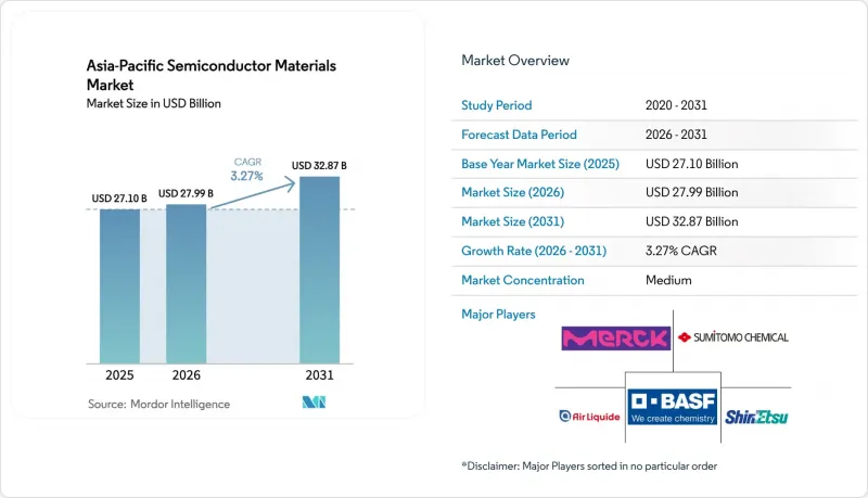
根據 Mordor Intelligence 預測,亞太半導體材料市場規模將從 2025 年的 271 億美元成長到 2026 年的 279.9 億美元,然後在 2031 年達到 328.7 億美元,2026 年至 2031 年的複合年成長率為 3.27%。
本報告依材料(矽晶圓、碳化矽、砷化鎵及其他)、應用(製造(製程化學品、光掩模)、其他)、封裝(基板、導線架、其他)、終端用戶產業(消費性電子、通訊和5G基礎設施、其他)以及地區進行細分。市場預測以美元計價。
亞太半導體材料市場趨勢與洞察
政府主導的「半導體主權基金」正在加速在中國、日本和韓國建設新型材料晶圓廠。
東北亞多個國家的政府正利用專案半導體基金津貼本地材料工廠,縮短認證週期,提高先進晶圓廠對本地生產材料的採用率。在韓國,京畿道正在建立一個投資4,710億美元的叢集,目標是到2030年實現關鍵化學品50%的自給自足。日本正將台積電熊本工廠的擴建計畫與國內光阻劑和晶圓供應商的聯合研發項目結合,而中國則在投資國產化學機械拋光(CMP)漿料、電子氣和氟化化學品。這些協調一致的投資即使在經濟低迷時期也能支撐穩定的需求,並為亞太半導體材料市場的成長提供結構性支撐。
中國和日本電動動力傳動系統對碳化矽和氮化鎵的應用迅速成長
為了降低傳導損耗並延長續航里程,電動車製造商正從矽MOSFET轉向碳化矽(SiC)和氮化鎵(GaN)功率裝置。中國垂直整合基板製造商的先驅已開始供應符合汽車級缺陷密度標準的200mm SiC晶圓,幫助本土OEM廠商獲得長期合約。同時,日本材料製造商也不斷提升用於汽車充電器的GaN-on-Si外延晶體品質。這項轉變正推動材料需求轉向寬能隙基板、外延氣體和高溫封裝,亞太半導體材料市場正突破傳統以矽為中心的格局。
矽和稀有金屬價格的波動給晶圓廠的利潤率帶來了壓力。
由於供應鏈高度集中在少數礦山,現貨矽晶圓和坩堝石英的價格波動幅度高達兩位數。同時,受出口許可限制的影響,鎵和鍺的價格也大幅上漲,迫使晶圓廠重新談判長期合約並對沖大宗商品價格波動風險。由於材料成本可佔晶圓製造現金成本的25%至30%,這些價格波動給盈利帶來壓力,並抑制了擴張計劃,導致亞太半導體材料市場對資本投資保持謹慎態度。
細分市場分析
2025年,矽晶圓在亞太半導體材料市場仍維持37.74%的最大市場佔有率,主要得益於5nm和3nm製程節點產能的提升。然而,碳化矽(SiC)顯然是市場成長的主要驅動力,隨著汽車電氣化和可再生能源電網對高電壓效率的需求,其複合年成長率(CAGR)高達9.08%。這種轉變擴大了滿足嚴格表面缺陷標準的寬能隙基板、氣體和拋光液的市場規模。氮化鎵(GaN)和砷化鎵(GaAs)材料在5G基地台和射頻前端的應用也日益廣泛,但基板成本仍然是其大規模生產的一大障礙。
製程創新使得200毫米碳化矽晶圓的試生產成為可能,其缺陷密度低於0.1cm⁻²,為汽車領域樹立了新的標竿。同時,韓國化學研究院在氫氟醚合成方面取得的突破性成果,提高了本地先進蝕刻化學品的供應穩定性。這些技術里程碑正在重塑亞太半導體材料市場的採購決策,因為單位成本降低、可靠性提高,進一步強化了「性能優先於價格」的概念。
其他好處
- Excel格式的市場預測(ME)表
- 3個月的分析師支持
目錄
第1章:引言
- 研究假設和市場定義
- 調查範圍
第2章:調查方法
第3章執行摘要
第4章 市場狀況
- 市場概覽
- 市場促進因素
- 政府主導的「半導體主權基金」正在加速在中國、日本和韓國建設新型材料晶圓廠。
- 中國和日本迅速採用碳化矽和氮化鎵作為電動車動力傳動系統
- 韓國和台灣地區Mini-LED和Micro-LED的大規模生產擴大,推動了對高純度金屬有機化合物的需求。
- 東協回流計畫:興建用於後端材料的待開發區化學工廠
- 對低全球暖化潛勢氟化氣體的管制將促進替代化學品的推廣。
- 異質整合(2.5D 和 3D IC)所需的新型底部填充材料和基板材料
- 市場限制因素
- 矽和稀有金屬價格的波動給晶圓廠的利潤率帶來了壓力。
- 由於美國和歐盟的出口限制,中國當地的材料認證出現延誤。
- 台灣和新加坡超純水短缺,阻礙了超純水產能的擴張。
- 在韓國,化工廠獲得環境、安全和衛生 (EHS) 許可證的過程變得越來越漫長。
- 工業生態系分析
- 技術展望
- 異質整合和背面電源
- 波特五力分析
第5章 市場規模與成長預測
- 材料
- 矽晶片
- 碳化矽(SiC)
- 砷化鎵(GaAs)
- 氮化鎵(GaN)
- 矽鍺(SiGe)
- 磷化銦(InP)
- 銅銦鎵硒(CIGS)
- 二硫化鉬(MoS2)
- 碲化鉍(Bi2Te3)
- 其他
- 透過使用
- 製造業
- 製程化學品
- 照片蒙版
- 電子氣體
- 光阻劑輔助材料
- 濺鍍靶
- 矽晶片
- CMP漿料和墊
- 其他製造材料
- 包裝
- 基板
- 導線架
- 陶瓷包裝
- 連接線
- 封裝樹脂
- 晶片黏接材料
- 其他包裝材料
- 製造業
- 按最終用戶行業分類
- 家用電器
- 通訊和5G基礎設施
- 工業和製造自動化
- 汽車出行(電動車、ADAS)
- 能源與公共產業(太陽能發電、電力轉換)
- 資料中心和高效能運算
- 醫療設備
- 其他
- 按地區
- 台灣
- 韓國
- 中國
- 日本
- 亞太其他地區
第6章 競爭情勢
- 市場集中度
- 策略性措施(併購、合資、擴大生產能力)
- 市佔率分析
- 公司簡介
- Shin-Etsu Chemical Co., Ltd.
- Showa Denko Materials Co., Ltd.
- Sumitomo Chemical Co., Ltd.
- Merck KGaA(incl. Versum Materials)
- Air Liquide SA
- BASF SE
- LG Chem Ltd.
- Indium Corporation
- Kyocera Corporation
- Henkel AG and Co. KGaA
- Dow Inc.
- JSR Corporation
- TOK(Tokyo Ohka Kogyo)
- DuPont de Nemours, Inc.
- Entegris, Inc.
- Linde plc
- SK Materials Co., Ltd.
- Toppan Photomask Co., Ltd.
- UTAC Holdings Ltd.
- Resonac
- Fujmi Corporation
- Mitsubishi Chemical Group Corp.
- Air Products and Chemicals, Inc.
第7章 市場機會與未來展望
According to Mordor Intelligence, the Asia-Pacific semiconductor materials market size is expected to grow from USD 27.10 billion in 2025 to USD 27.99 billion in 2026 and is forecast to reach USD 32.87 billion by 2031 at 3.27% CAGR over 2026-2031.
This report is Segmented by Material (Silicon Wafers, Silicon Carbide, Gallium Arsenide, and More), Application (Fabrication [Process Chemicals, Photomasks], and More), Packaging (Substrates, Lead Frames, and More), End-User Industry (Consumer Electronics, Telecommunication and 5G Infrastructure, and More), and Geography. The Market Forecasts are Provided in Terms of Value (USD).
Asia-Pacific Semiconductor Materials Market Trends and Insights
Government-backed Chip Sovereignty Funds Accelerating New Material Fabs in China, Japan and Korea
Several Northeast-Asian governments are using dedicated chip funds to subsidize local material plants, shortening qualification cycles and lifting regional content in leading-edge fabs. In Korea, a USD 471 billion cluster in Gyeonggi Province targets 50% self-sufficiency in critical chemistries by 2030. Japan is tying TSMC's Kumamoto expansion to joint R&D programs with domestic photoresist and wafer suppliers, while China is channeling capital toward indigenous CMP slurries, electronic gases and fluorochemicals. These coordinated investments underpin steady demand even during cyclical downturns, giving the Asia-Pacific semiconductor materials market a structural growth floor.
Surge in SiC and GaN Adoption for EV Powertrains Across China and Japan
Electric-vehicle makers are shifting from silicon MOSFETs to SiC and GaN power devices to cut conduction losses and boost driving range. Chinese vertically integrated substrate pioneers have begun supplying 200 mm SiC wafers that meet automotive-grade defect density thresholds, helping local OEMs lock-in long-term contracts. Japanese material houses are parallel-tracking crystalline-quality improvements for GaN-on-Si epitaxy to serve on-board chargers. This transition is tilting material demand toward wide-bandgap substrates, epitaxial gases and high-temperature encapsulants, broadening the Asia-Pacific semiconductor materials market beyond its silicon core.
Volatile Silicon and Rare-Metal Prices Squeezing Fab Margins
Spot silicon-wafers and crucible-grade quartz have exhibited double-digit price swings amid tight supply chains concentrated in a handful of mines. Parallel spikes in gallium and germanium prices, following export-license restrictions, are forcing fabs to re-negotiate long-term contracts and hedge commodity exposure. Because material outlays can represent 25-30% of wafer-fabrication cash costs, these fluctuations compress profitability and temper expansion plans, keeping the Asia-Pacific semiconductor materials market on a cautious capital-expenditure footing.
Other drivers and restraints analyzed in the detailed report include:
- Mini/Micro-LED Ramp-up Driving Demand for High-Purity Metal-Organics in Korea and Taiwan
- ASEAN Re-shoring Initiatives Creating Green-field Chemical Plants for Backend Materials
- US/EU Export Controls Delaying Material Qualification in Mainland China
For complete list of drivers and restraints, kindly check the Table Of Contents.
Segment Analysis
Silicon Wafers retained the largest 37.74% share of the Asia-Pacific semiconductor materials market in 2025, supported by capacity additions at 5 nm and 3 nm nodes. Yet Silicon Carbide is the clear growth engine, expanding at 9.08% CAGR as vehicle electrification and renewable grids demand high-voltage efficiency. This shift is enlarging the Asia-Pacific semiconductor materials market size for wide-bandgap substrates, gases and polishing slurries that meet stringent surface-defect criteria. GaN and GaAs materials are also gaining traction for 5G base-stations and RF front-ends, even though substrate costs remain a cap on volume adoption.
Process innovation is bringing 200 mm SiC wafers to pilot scale, with defect densities below 0.1 cm-2 setting new automotive benchmarks. At the same time, the Korea Research Institute of Chemical Technology's breakthrough in hydrofluoroether synthesis improves local supply security for advanced etch chemistries. As these technical milestones reduce unit costs and raise reliability, they reinforce a performance-over-price paradigm that re-shapes procurement decisions within the Asia-Pacific semiconductor materials market.
Complete Report Scope:
- By Material
- Silicon Wafers
- Silicon Carbide (SiC)
- Gallium Arsenide (GaAs)
- Gallium Nitride (GaN)
- Silicon Germanium (SiGe)
- Indium Phosphide (InP)
- Copper Indium Gallium Selenide (CIGS)
- Molybdenum Disulfide (MoS?)
- Bismuth Telluride (Bi?Te?)
- Other Materials
- By Application
- Fabrication
- Process Chemicals
- Photomasks
- Electronic Gases
- Photoresist Ancillaries
- Sputtering Targets
- Silicon Wafers
- CMP Slurries and Pads
- Other Fabrication Materials
- Packaging
- Substrates
- Lead Frames
- Ceramic Packages
- Bonding Wire
- Encapsulation Resins
- Die-Attach Materials
- Other Packaging Materials
- Fabrication
- By End-user Industry
- Consumer Electronics
- Telecommunication and 5G Infrastructure
- Industrial and Manufacturing Automation
- Automotive and Mobility (EV, ADAS)
- Energy and Utility (Solar, Power Conversion)
- Data Centers and HPC
- Healthcare Devices
- Others
- By Geography
- Taiwan
- South Korea
- China
- Japan
- Rest of Asia-Pacific
List of Companies Covered in this Report:
- Shin-Etsu Chemical Co., Ltd.
- Showa Denko Materials Co., Ltd.
- Sumitomo Chemical Co., Ltd.
- Merck KGaA (incl. Versum Materials)
- Air Liquide S.A.
- BASF SE
- LG Chem Ltd.
- Indium Corporation
- Kyocera Corporation
- Henkel AG and Co. KGaA
- Dow Inc.
- JSR Corporation
- TOK (Tokyo Ohka Kogyo)
- DuPont de Nemours, Inc.
- Entegris, Inc.
- Linde plc
- SK Materials Co., Ltd.
- Toppan Photomask Co., Ltd.
- UTAC Holdings Ltd.
- Resonac
- Fujmi Corporation
- Mitsubishi Chemical Group Corp.
- Air Products and Chemicals, Inc.
Additional Benefits:
- The market estimate (ME) sheet in Excel format
- 3 months of analyst support
TABLE OF CONTENTS
1 INTRODUCTION
- 1.1 Study Assumptions and Market Definition
- 1.2 Scope of the Study
2 RESEARCH METHODOLOGY
3 EXECUTIVE SUMMARY
4 MARKET LANDSCAPE
- 4.1 Market Overview
- 4.2 Market Drivers
- 4.2.1 Government-backed Chip Sovereignty Funds Accelerating New Material Fabs in China, Japan and Korea
- 4.2.2 Surge in SiC and GaN Adoption for EV Powertrains Across China and Japan
- 4.2.3 Mini/Micro-LED Ramp-up Driving Demand for High-Purity Metal-Organics in Korea and Taiwan
- 4.2.4 ASEAN Re-shoring Initiatives Creating Green-field Chemical Plants for Backend Materials
- 4.2.5 Low-GWP Fluorinated Gas Mandates Boosting Replacement Chemistries
- 4.2.6 Heterogeneous Integration (2.5D/3D IC) Needs Novel Under-fill and Substrate Materials
- 4.3 Market Restraints
- 4.3.1 Volatile Silicon and Rare-Metal Prices Squeezing Fab Margins
- 4.3.2 US/EU Export Controls Delaying Material Qualification in Mainland China
- 4.3.3 Ultrapure-Water Scarcity in Taiwan and Singapore Hindering capacity Adds
- 4.3.4 Lengthy EHS Permitting for Chemical Plants in Korea
- 4.4 Industry Ecosystem Analysis
- 4.5 Technological Outlook
- 4.5.1 Heterogeneous Integration and Back-side Power Delivery
- 4.6 Porter's Five Forces Analysis
- 4.6.1 Bargaining Power of Suppliers
- 4.6.2 Bargaining Power of Buyers
- 4.6.3 Threat of New Entrants
- 4.6.4 Threat of Substitutes
- 4.6.5 Competitive Rivalry
5 MARKET SIZE AND GROWTH FORECASTS (VALUES)
- 5.1 By Material
- 5.1.1 Silicon Wafers
- 5.1.2 Silicon Carbide (SiC)
- 5.1.3 Gallium Arsenide (GaAs)
- 5.1.4 Gallium Nitride (GaN)
- 5.1.5 Silicon Germanium (SiGe)
- 5.1.6 Indium Phosphide (InP)
- 5.1.7 Copper Indium Gallium Selenide (CIGS)
- 5.1.8 Molybdenum Disulfide (MoS?)
- 5.1.9 Bismuth Telluride (Bi?Te?)
- 5.1.10 Other Materials
- 5.2 By Application
- 5.2.1 Fabrication
- 5.2.1.1 Process Chemicals
- 5.2.1.2 Photomasks
- 5.2.1.3 Electronic Gases
- 5.2.1.4 Photoresist Ancillaries
- 5.2.1.5 Sputtering Targets
- 5.2.1.6 Silicon Wafers
- 5.2.1.7 CMP Slurries and Pads
- 5.2.1.8 Other Fabrication Materials
- 5.2.2 Packaging
- 5.2.2.1 Substrates
- 5.2.2.2 Lead Frames
- 5.2.2.3 Ceramic Packages
- 5.2.2.4 Bonding Wire
- 5.2.2.5 Encapsulation Resins
- 5.2.2.6 Die-Attach Materials
- 5.2.2.7 Other Packaging Materials
- 5.2.1 Fabrication
- 5.3 By End-user Industry
- 5.3.1 Consumer Electronics
- 5.3.2 Telecommunication and 5G Infrastructure
- 5.3.3 Industrial and Manufacturing Automation
- 5.3.4 Automotive and Mobility (EV, ADAS)
- 5.3.5 Energy and Utility (Solar, Power Conversion)
- 5.3.6 Data Centers and HPC
- 5.3.7 Healthcare Devices
- 5.3.8 Others
- 5.4 By Geography
- 5.4.1 Taiwan
- 5.4.2 South Korea
- 5.4.3 China
- 5.4.4 Japan
- 5.4.5 Rest of Asia-Pacific
6 COMPETITIVE LANDSCAPE
- 6.1 Market Concentration
- 6.2 Strategic Moves (M&A, JVs, capacity Expansions)
- 6.3 Market Share Analysis
- 6.4 Company Profiles (includes Global Overview, Market Level Overview, Core Segments, Financials, Strategic Information, Market Rank/Share, Products and Services, Recent Developments)
- 6.4.1 Shin-Etsu Chemical Co., Ltd.
- 6.4.2 Showa Denko Materials Co., Ltd.
- 6.4.3 Sumitomo Chemical Co., Ltd.
- 6.4.4 Merck KGaA (incl. Versum Materials)
- 6.4.5 Air Liquide S.A.
- 6.4.6 BASF SE
- 6.4.7 LG Chem Ltd.
- 6.4.8 Indium Corporation
- 6.4.9 Kyocera Corporation
- 6.4.10 Henkel AG and Co. KGaA
- 6.4.11 Dow Inc.
- 6.4.12 JSR Corporation
- 6.4.13 TOK (Tokyo Ohka Kogyo)
- 6.4.14 DuPont de Nemours, Inc.
- 6.4.15 Entegris, Inc.
- 6.4.16 Linde plc
- 6.4.17 SK Materials Co., Ltd.
- 6.4.18 Toppan Photomask Co., Ltd.
- 6.4.19 UTAC Holdings Ltd.
- 6.4.20 Resonac
- 6.4.21 Fujmi Corporation
- 6.4.22 Mitsubishi Chemical Group Corp.
- 6.4.23 Air Products and Chemicals, Inc.
7 MARKET OPPORTUNITIES AND FUTURE OUTLOOK
- 7.1 White-space and Unmet-Need Assessment

 半導體材料市場:預測至 2034 年-按材料類別、製造流程、晶圓尺寸、半導體類型、終端應用產業、技術節點、分銷管道和地區分類的全球分析
 半導體材料市場-全球產業規模、佔有率、趨勢、機會和預測:按應用、封裝、終端用戶產業、地區和競爭格局分類,2021-2031年自旋電子材料市場預測至2034年-按材料類型、裝置類型、應用、技術、最終用戶和地區分類的全球分析
 全球半導體陶瓷聚焦環市場報告:競爭分析與區域機會(2026-2032 年)
 半導體材料市場報告:按材料、應用、終端用戶產業和地區分類(2026-2034 年)
 碳化矽基板市場報告:趨勢、預測與競爭分析(至2035年)
 半導體管市場:按材料、應用和最終用途分類-2026-2032年全球市場預測半導體材料市場:材料類型、晶圓尺寸、應用和終端用戶產業分類-2026-2032年全球市場預測
 全球先進鑽石材料與技術市場(2026-2036)
 半導體用鑽石材料市場規模、佔有率及成長分析(依材料類型、形狀、應用、終端用戶產業及地區分類)-2026-2033年產業預測