


 |
市場調查報告書
商品編碼
2115045
外延設備:市場佔有率分析、產業趨勢與統計、成長預測(2026-2031)Epitaxy Equipment - Market Share Analysis, Industry Trends & Statistics, Growth Forecasts (2026 - 2031) |
||||||

※ 本網頁內容可能與最新版本有所差異。詳細情況請與我們聯繫。
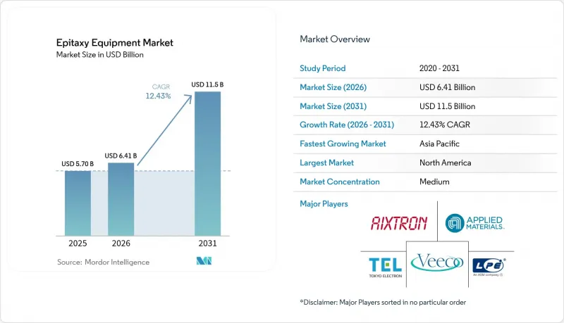
據 Mordor Intelligence 稱,2025 年外延元件市場價值為 57 億美元,預計到 2031 年將達到 115 億美元,而 2026 年為 64.1 億美元,預測期(2026-2031 年)的複合年成長率為 12.43%。
本報告按技術(例如,金屬有機化學氣相沉積 (MOCVD)、氫化物氣相外延 (HVPE))、應用(例如,光電、半導體)、晶圓尺寸(4 英寸以下、6 英寸、8 英寸、12 英寸、12 英寸以上)、材料(III-V 族系統(GaAs、InP)、GaN、SiC 等地區進行細分。市場預測以美元 (USD) 為單位。
全球外延設備市場趨勢與洞察
高亮度LED的需求日益成長
高階顯示器和汽車照明領域對MicroLED和mini-LED的廣泛應用,推動了三安光電等LED製造商的多系統MOCVD訂單成長。降低6吋和8吋晶圓的缺陷密度對於提高產能至關重要,這也使得Veeco的Lumina平台訂單積壓量居高不下。此外,汽車日間行車燈和自我調整遠光燈也需要更高的光通量,從而提高了GaN層均勻性的外延性能要求。這些因素共同作用,形成了可預測的3-4年設備更新周期,增強了中期出貨前景。
電動車動力傳動系統的快速電氣化
汽車製造商正朝著 800V 架構邁進,加速了碳化矽 (SiC) MOSFET 和二極體的採用,這些裝置需要生長在 1600 度C以上的外延層。在博世公司根據《晶片技術創新法案》(CHIPS Act) 獲得 2.25 億美元津貼用於其位於阿拉巴馬州的 SiC 生產線後,東京電子的高溫 CVD 設備訂單有所增加。 SiC基板從 150 毫米增加到 200 毫米,使得全球晶圓廠必須投資新設備並引入改裝套件。功率模組的良率對微管密度和摻雜漂移極為敏感,因此元件製造商只有在經過數月的製程配方合作開發後才會下單,這導致收入確認週期較長,但其市場基礎正在穩步發展。
反應器設計的複雜性
隨著製造商對雙材料和300毫米腔室的需求不斷成長,計算流體力學(CFD) 模型必須同時考慮層流氣體流動和陡峭的溫度梯度,這導致研發週期延長。供應商正在整合多區加熱器、電動噴射器集氣室和原位橢偏儀,這增加了材料清單(BOM) 成本和軟體檢驗成本。這些技術難題正在延緩收入成長,並提高了後進企業的進入門檻。
細分市場分析
金屬有機化學氣相沉積(MOCVD)憑藉在LED和GaN功率元件領域的強大地位,預計2025年將佔據外延設備市場46.73%的佔有率。此細分市場的規模允許晶圓尺寸逐步擴大而無需進行大規模重新設計,從而確保持續的重複訂單。同時,遠程等離子體化學氣相沉積(RPCVD)預計將以13.35%的複合年成長率成長,透過低溫製程和更精確的界面控制,使其能夠應用於易碎基板。 RPCVD外延設備市場預計到2031年將達到15.9億美元。分子束外延(MBE)和氫化物氣相外延(HPVE)雖然仍屬於小眾領域,但前者適用於生產超高純度異質結構,後者適用於厚膜GaN基板。另一方面,高溫化學氣相沉積(HT-CVD)正逐漸成為製備厚度超過20µm的SiC層的主流技術。在所有平台上,供應商將自身的多材料柔軟性定位為優勢,以應對未來的技術節點。
第二個競爭重點在於先進的製程控制堆疊。一級晶圓廠對封閉回路型發射率校正溫度測量和基於機器學習的故障檢測的需求日益成長,這些功能最容易對MOCVD和RPCVD架構進行改造。因此,平均售價的成長速度超過了銷量成長速度,即使在LED細分市場充斥著入門級中國製造設備的背景下,利潤率也得到了提升。開放平台軟體生態系統也正在成為一項差異化優勢,使晶圓廠能夠跨硬體供應商移植流程,並縮短認證週期。
預計到2025年,化合物半導體裝置的製造將佔總銷售額的52.10%,主要驅動力來自射頻放大器、用於雷射雷達的垂直腔面發射雷射(VCSEL)以及光電收發器。然而,成長最快的細分市場是用於電動車逆變器和通訊電源的寬能隙材料,年成長率高達13.52%。寬能隙應用的外延設備市場預計到2025年將達到22.8億美元,到2031年可能超過48.8億美元。光電領域,特別是磷化銦(InP)光子積體電路(PIC),正受益於超大規模資料中心的光子技術, 連貫公司在德克薩斯州工廠的InP產量增加了兩倍便是最好的證明。微機電系統(MEMS)鑄造雖然規模較小,但其依賴於客製化的外延堆疊結構來製造壓力感測器和射頻濾波器,從而開闢了一個穩定且專業的設備市場。
終端應用的多樣化要求設備製造商提供可在同一晶圓廠內配置的模組化反應器,用於製備SiC、GaN和InP等材料。這種適應性有助於保護資本投資預算免受需求快速波動的影響。同時,設備供應商和化學品供應商之間的合作旨在共同最佳化前驅體流動動力學、改善薄膜化學計量比,並實現諸如GaN垂直電晶體等新型裝置結構。
區域分析
北美地區,尤其是在德克薩斯州、亞利桑那州和紐約州北部等叢集的支撐下,預計到2025年將保持43.25%的銷售額佔有率。 《晶片法案》(CHIPS Act)的資金正被用於待開發區晶圓廠和棕地的升級改造,從而支撐對國內外延技術能力的長期需求。例如,相干公司(連貫)位於謝爾曼的園區將磷化銦(InP)裝置的產量提高了兩倍,以滿足人工智慧光鏈路的需求。政府合約中包含的在地採購規則傾向於本地供應商,儘管外匯波動削弱了出口競爭力,但這些規則仍然增強了訂單供應。
亞太地區是成長最快的市場,預計到2031年將以15.22%的複合年成長率成長。中國LED製造商,例如HC SemiTek,已累積了超過2500套MOCVD系統,在產量方面佔據主導地位。同時,韓國主要記憶體公司正在投資CXL光電和HBM電源的化合物半導體藍圖,進一步擴大了該地區的潛在市場。東京電子2025年第一季6,545億日圓的銷售額清晰地顯示了對上游供應商的連鎖反應。
歐洲的重點在於汽車電氣化和建造強大的航太供應鏈。基於「歐洲晶片法」的計畫為德國和瑞典的碳化矽外延製造提供補貼,而法國的研究機構正在試運行用於雷達和衛星有效載荷的200毫米氮化鎵矽基(GaN-on-Si)生產線。當地的環境法規正在加速採用低全球暖化潛勢的製程氣體,歐洲的製造業也擴大採用改良的廢氣處理模組。儘管該地區在產量方面落後於其他地區,但在高利潤率的專用設備和專門用於量子計算材料的研究級分子束外延(MBE)系統方面卻表現出色。
其他好處:
- Excel格式的市場預測(ME)表
- 3個月的分析師支持
目錄
第1章:引言
- 研究假設和市場定義
- 調查範圍
第2章:調查方法
第3章執行摘要
第4章 市場狀況
- 市場概覽
- 市場促進因素
- 高亮度LED的需求日益成長
- 電動車動力傳動系統的快速電氣化
- 5G/6G化合物半導體前端模組的擴展
- 政府推出支持措施,擴大SiC/GaN產能
- 採用氧化鎵(B-Ga₂O₃)元件
- 向 8 英寸和 12 英寸 GaN-on-Si 外延生產線過渡
- 市場限制因素
- 核子反應爐設計的複雜性
- 特殊前驅物的價格與供應波動
- IDM 和鑄造業工具認證週期延長。
- 對下一代高溫核子反應爐進行大量資本投資
- 產業供應鏈分析
- 監理情勢
- 技術展望
- 宏觀經濟因素的影響
- 波特五力分析
第5章 市場規模與成長預測
- 透過技術
- 金屬有機化學氣相沉積(MOCVD)
- 氫化物氣相外延(HVPE)
- 高溫化學氣相沉積(HT-CVD)
- 分子束外延(MBE)
- 遠程等離子化學氣相沉積(RPCVD)
- 透過使用
- 光電
- 半導體
- 寬能隙材料
- 微電子機械系統(MEMS)
- 其他
- 按晶圓尺寸
- 4英吋或更小
- 6吋
- 8吋
- 12英吋
- 超過 12 英寸
- 材料
- III-V族(GaAs、InP)
- GaN
- SiC
- 其他
- 按地區
- 北美洲
- 美國
- 加拿大
- 墨西哥
- 南美洲
- 巴西
- 阿根廷
- 其他南美國家
- 歐洲
- 德國
- 英國
- 法國
- 義大利
- 西班牙
- 俄羅斯
- 其他歐洲國家
- 亞太地區
- 中國
- 日本
- 印度
- 韓國
- 東南亞
- 其他亞太國家
- 中東和非洲
- 中東
- 沙烏地阿拉伯
- 阿拉伯聯合大公國
- 土耳其
- 其他中東國家
- 非洲
- 南非
- 奈及利亞
- 其他非洲國家
- 中東
- 北美洲
第6章 競爭情勢
- 市場集中度
- 策略趨勢
- 市佔率分析
- 公司簡介
- Aixtron SE
- Applied Materials, Inc.
- Tokyo Electron Limited
- Veeco Instruments Inc.
- LPE SpA
- NuFlare Technology, Inc.(Toshiba Electronic Devices and Storage Corp.)
- II-VI Incorporated(Coherent Corp.)
- Intelligent Epitaxy Technology, Inc.
- DOWA Electronics Materials Co., Ltd.
- Siltronic AG
- RIBER SA
- Taiyo Nippon Sanso Corporation
- Chengdu Alight Optoelectronics Technology Co., Ltd.
- Advanced Epi Materials and Devices UK Ltd.
- NAURA Technology Group Co., Ltd.
- Shenzhen Topraysolar Co., Ltd.
- Suzhou Nano Epitaxy Inc.
- VEECO-Suzhou(CMI Suzhou)
- Jiangsu J-PEC Technology Co., Ltd.
- SkyWater Technology Foundry
第7章 市場機會與未來展望
According to Mordor Intelligence, the epitaxy equipment market size was valued at USD 5.7 billion in 2025 and estimated to grow from USD 6.41 billion in 2026 to reach USD 11.5 billion by 2031, at a CAGR of 12.43% during the forecast period (2026-2031).
This report is Segmented by Technology (Metal-Organic Chemical Vapor Deposition (MOCVD), Hydride Vapor Phase Epitaxy (HVPE), and More), Application (Photonics, Semiconductors, and More), Wafer Size (Less Than or Equal To 4-Inch, 6-Inch, 8-Inch, 12-Inch, and Greater Than 12-Inch), Material (III-V (GaAs, Inp), Gan, Sic and Others), and Geography. The Market Forecasts are Provided in Terms of Value (USD).
Global Epitaxy Equipment Market Trends and Insights
Increasing Demand for High-Brightness LEDs
MicroLED and mini-LED adoption in premium displays and automotive lighting causes LED makers such as San'an Optoelectronics to book multi-system MOCVD orders. Throughput upgrades must coincide with lower defect density across 6- and 8-inch wafers, keeping Veeco's Lumina platform backlog elevated. Automotive daytime-running lamps and adaptive-beam headlamps also require higher luminous flux, which in turn pushes epitaxy specifications for GaN layer uniformity. These combined forces translate into a predictable equipment-replacement cycle every three to four years, fortifying mid-term shipment trajectories.
Rapid Electrification of Powertrains in EVs
Automakers migrate to 800 V architectures, accelerating silicon-carbide MOSFET and diode uptake that demands epitaxial layers grown at >=1,600 °C. Tokyo Electron's high-temperature CVD tool bookings rose in tandem with Bosch securing USD 225 million in CHIPS Act grants for Alabama SiC lines. The move from 150 mm to 200 mm SiC substrates compels both new-tool investments and retrofit kits across global fabs. Because power-module yields are hypersensitive to micropipe density and doping drift, device makers award purchase orders only after months of process-recipe co-engineering, extending revenue recognition yet building an entrenched installed base.
Complexities Associated With Reactor Design
As fabs request dual-material or 300 mm chambers, computational-fluid-dynamics models must reconcile laminar gas flow with sharp temperature gradients, lengthening R&D cycles. Suppliers therefore integrate multi-zone heaters, motorized injector plenums, and in-situ spectroscopic ellipsometry, driving up bill-of-materials and software validation costs. These engineering hurdles defer revenue and raise the entry barrier for latecomers.
Other drivers and restraints analyzed in the detailed report include:
- Expansion of 5G/6G Compound-Semiconductor Front-End Modules
- Government Incentives for SiC/GaN Capacity Build-Out
- Volatile Prices and Supply of Specialty Precursors
For complete list of drivers and restraints, kindly check the Table Of Contents.
Segment Analysis
Metal-organic chemical vapor deposition occupied 46.73% of the epitaxy equipment market share in 2025 on the back of its entrenched position in LED and GaN power devices. The segment's scale enables incremental wafer-size increases without catastrophic redesign, sustaining repeat orders. Remote-plasma CVD, though, is projected to post a 13.35% CAGR as lower-temperature processing opens doors to fragile substrates and tighter interface control. The epitaxy equipment market size for RPCVD tools is expected to reach USD 1.59 billion by 2031. MBE and hydride vapor-phase epitaxy remain niche, favored for ultra-pure heterostructures and thick GaN substrates, respectively, while HT-CVD dominates SiC layers exceeding 20 µm thickness. Across all platforms, suppliers position multi-material flexibility as a hedge against future technology nodes.
A second competitive angle revolves around advanced process-control stacks. Tier-one fabs increasingly insist on closed-loop emissivity-corrected pyrometry and machine-learning fault detection, features most readily retrofitted to MOCVD and RPCVD architectures. Consequently, average selling prices rise faster than unit volumes, cushioning margins even as entry-level Chinese tools crowd the LED subsegment. Open-platform software ecosystems emerge as another differentiator, enabling fabs to port recipes across vendor hardware and thus shorten qualification cycles.
Compound-semiconductor device manufacturing captured 52.10% of 2025 revenue, driven by RF amplifiers, LiDAR VCSELs, and photonics transceivers. Yet the fastest uplift stems from wide-bandgap materials used in electric-vehicle inverters and telecom power supplies, advancing 13.52% annually. The epitaxy equipment market size for wide-bandgap applications stood at USD 2.28 billion in 2025 and could surpass USD 4.88 billion by 2031. Photonics lines, especially indium-phosphide PICs, benefit from hyperscale data-center optics, evidenced by Coherent tripling InP output at its Texas site. MEMS foundries, though smaller, rely on custom epitaxial stacks for pressure sensors and RF filters, carving a steady yet specialized equipment niche.
The diversity of end-use cases forces equipment makers to supply modular reactors configurable between SiC, GaN, and InP within the same fab footprint. Such adaptability protects capex budgets from sudden demand shifts. Concurrently, partnerships between tool vendors and chemical suppliers aim to co-optimize precursor flow dynamics, improving film stoichiometry and unlocking new device architectures such as GaN vertical transistors.
Complete Report Scope:
- By Technology
- Metal-Organic Chemical Vapor Deposition (MOCVD)
- Hydride Vapor Phase Epitaxy (HVPE)
- High-Temperature Chemical Vapor Deposition (HT-CVD)
- Molecular Beam Epitaxy (MBE)
- Remote-Plasma CVD (RPCVD)
- By Application
- Photonics
- Semiconductors
- Wide-Bandgap Materials
- Micro-Electro-Mechanical Systems (MEMS)
- Others
- By Wafer Size
- Less than or Equal to 4-inch
- 6-inch
- 8-inch
- 12-inch
- Greater than 12-inch
- By Material
- III-V (GaAs, InP)
- GaN
- SiC
- Others
- By Geography
- North America
- United States
- Canada
- Mexico
- South America
- Brazil
- Argentina
- Rest of South America
- Europe
- Germany
- United Kingdom
- France
- Italy
- Spain
- Russia
- Rest of Europe
- Asia-Pacific
- China
- Japan
- India
- South Korea
- South-East Asia
- Rest of Asia-Pacific
- Middle East and Africa
- Middle East
- Saudi Arabia
- United Arab Emirates
- Turkey
- Rest of Middle East
- Africa
- South Africa
- Nigeria
- Rest of Africa
- Middle East
- North America
Geography Analysis
North America preserved a 43.25% revenue share in 2025, supported by dense clusters in Texas, Arizona, and upstate New York. CHIPS Act disbursements flow to both greenfield fabs and brownfield upgrades, anchoring long-term demand for domestic epitaxy capacity. Coherent's Sherman campus, for instance, tripled InP device output to meet AI optical-link demand. Local sourcing rules embedded in government contracts tilt procurement toward resident suppliers, bolstering order pipelines even as exchange-rate swings temper export competitiveness.
Asia-Pacific represents the fastest-growing theater with a 15.22% CAGR through 2031. Chinese LED houses such as HC SemiTek accumulate MOCVD install bases that already exceed 2,500 reactors, driving unit-volume leadership. Simultaneously, South Korean memory giants invest in compound-semiconductor roadmaps for CXL photonics and HBM power delivery, widening the regional addressable market. Tokyo Electron's net sales climb to YEN 654.5 billion in Q1 2025 underscores the pull-through effect on upstream tool vendors.
Europe concentrates on automotive electrification and resilient aerospace supply chains. Programs under the European Chips Act channel subsidies to SiC epi fabs in Germany and Sweden, while French institutes pilot 200 mm GaN-on-Si lines for radar and satellite payloads. Local environmental regulations expedite adoption of low-global-warming-potential process gases, prompting European fabs to specify upgraded abatement modules. Although the region trails in unit volumes, it excels in high-margin specialty tools and research-grade MBE systems tailored for quantum-computing materials.
- Aixtron SE
- Applied Materials, Inc.
- Tokyo Electron Limited
- Veeco Instruments Inc.
- LPE S.p.A.
- NuFlare Technology, Inc. (Toshiba Electronic Devices and Storage Corp.)
- II-VI Incorporated (Coherent Corp.)
- Intelligent Epitaxy Technology, Inc.
- DOWA Electronics Materials Co., Ltd.
- Siltronic AG
- RIBER S.A.
- Taiyo Nippon Sanso Corporation
- Chengdu Alight Optoelectronics Technology Co., Ltd.
- Advanced Epi Materials and Devices UK Ltd.
- NAURA Technology Group Co., Ltd.
- Shenzhen Topraysolar Co., Ltd.
- Suzhou Nano Epitaxy Inc.
- VEECO-Suzhou (CMI Suzhou)
- Jiangsu J-PEC Technology Co., Ltd.
- SkyWater Technology Foundry
Additional Benefits:
- The market estimate (ME) sheet in Excel format
- 3 months of analyst support
TABLE OF CONTENTS
1 INTRODUCTION
- 1.1 Study Assumptions and Market Definition
- 1.2 Scope of the Study
2 RESEARCH METHODOLOGY
3 EXECUTIVE SUMMARY
4 MARKET LANDSCAPE
- 4.1 Market Overview
- 4.2 Market Drivers
- 4.2.1 Increasing demand for high-brightness LEDs
- 4.2.2 Rapid electrification of powertrains in EVs
- 4.2.3 Expansion of 5G/6G compound-semiconductor front-end modules
- 4.2.4 Government incentives for SiC/GaN capacity build-out
- 4.2.5 Adoption of gallium-oxide (B-Ga2O3) devices
- 4.2.6 Transition to 8- and 12-inch GaN-on-Si epitaxy lines
- 4.3 Market Restraints
- 4.3.1 Complexities associated with reactor design
- 4.3.2 Volatile prices and supply of specialty precursors
- 4.3.3 Lengthy tool qualification cycles at IDMs and foundries
- 4.3.4 High capex for next-gen high-temperature reactors
- 4.4 Industry Supply Chain Analysis
- 4.5 Regulatory Landscape
- 4.6 Technological Outlook
- 4.7 Impact of Macroeconomic Factors
- 4.8 Porter's Five Forces Analysis
- 4.8.1 Threat of New Entrants
- 4.8.2 Bargaining Power of Buyers/Consumers
- 4.8.3 Bargaining Power of Suppliers
- 4.8.4 Threat of Substitute Products
- 4.8.5 Intensity of Competitive Rivalry
5 MARKET SIZE AND GROWTH FORECASTS (VALUE)
- 5.1 By Technology
- 5.1.1 Metal-Organic Chemical Vapor Deposition (MOCVD)
- 5.1.2 Hydride Vapor Phase Epitaxy (HVPE)
- 5.1.3 High-Temperature Chemical Vapor Deposition (HT-CVD)
- 5.1.4 Molecular Beam Epitaxy (MBE)
- 5.1.5 Remote-Plasma CVD (RPCVD)
- 5.2 By Application
- 5.2.1 Photonics
- 5.2.2 Semiconductors
- 5.2.3 Wide-Bandgap Materials
- 5.2.4 Micro-Electro-Mechanical Systems (MEMS)
- 5.2.5 Others
- 5.3 By Wafer Size
- 5.3.1 Less than or Equal to 4-inch
- 5.3.2 6-inch
- 5.3.3 8-inch
- 5.3.4 12-inch
- 5.3.5 Greater than 12-inch
- 5.4 By Material
- 5.4.1 III-V (GaAs, InP)
- 5.4.2 GaN
- 5.4.3 SiC
- 5.4.4 Others
- 5.5 By Geography
- 5.5.1 North America
- 5.5.1.1 United States
- 5.5.1.2 Canada
- 5.5.1.3 Mexico
- 5.5.2 South America
- 5.5.2.1 Brazil
- 5.5.2.2 Argentina
- 5.5.2.3 Rest of South America
- 5.5.3 Europe
- 5.5.3.1 Germany
- 5.5.3.2 United Kingdom
- 5.5.3.3 France
- 5.5.3.4 Italy
- 5.5.3.5 Spain
- 5.5.3.6 Russia
- 5.5.3.7 Rest of Europe
- 5.5.4 Asia-Pacific
- 5.5.4.1 China
- 5.5.4.2 Japan
- 5.5.4.3 India
- 5.5.4.4 South Korea
- 5.5.4.5 South-East Asia
- 5.5.4.6 Rest of Asia-Pacific
- 5.5.5 Middle East and Africa
- 5.5.5.1 Middle East
- 5.5.5.1.1 Saudi Arabia
- 5.5.5.1.2 United Arab Emirates
- 5.5.5.1.3 Turkey
- 5.5.5.1.4 Rest of Middle East
- 5.5.5.2 Africa
- 5.5.5.2.1 South Africa
- 5.5.5.2.2 Nigeria
- 5.5.5.2.3 Rest of Africa
- 5.5.5.1 Middle East
- 5.5.1 North America
6 COMPETITIVE LANDSCAPE
- 6.1 Market Concentration
- 6.2 Strategic Moves
- 6.3 Market Share Analysis
- 6.4 Company Profiles (includes Global level Overview, Market level overview, Core Segments, Financials as available, Strategic Information, Market Rank/Share for key companies, Products and Services, and Recent Developments)
- 6.4.1 Aixtron SE
- 6.4.2 Applied Materials, Inc.
- 6.4.3 Tokyo Electron Limited
- 6.4.4 Veeco Instruments Inc.
- 6.4.5 LPE S.p.A.
- 6.4.6 NuFlare Technology, Inc. (Toshiba Electronic Devices and Storage Corp.)
- 6.4.7 II-VI Incorporated (Coherent Corp.)
- 6.4.8 Intelligent Epitaxy Technology, Inc.
- 6.4.9 DOWA Electronics Materials Co., Ltd.
- 6.4.10 Siltronic AG
- 6.4.11 RIBER S.A.
- 6.4.12 Taiyo Nippon Sanso Corporation
- 6.4.13 Chengdu Alight Optoelectronics Technology Co., Ltd.
- 6.4.14 Advanced Epi Materials and Devices UK Ltd.
- 6.4.15 NAURA Technology Group Co., Ltd.
- 6.4.16 Shenzhen Topraysolar Co., Ltd.
- 6.4.17 Suzhou Nano Epitaxy Inc.
- 6.4.18 VEECO-Suzhou (CMI Suzhou)
- 6.4.19 Jiangsu J-PEC Technology Co., Ltd.
- 6.4.20 SkyWater Technology Foundry
7 MARKET OPPORTUNITIES AND FUTURE OUTLOOK
- 7.1 White-space and Unmet-need Assessment

 外延設備市場:依技術、應用、晶圓尺寸、材料、國家及地區分類-全球產業分析、市場規模、市場佔有率及2026年至2033年預測
 全球分子束外延市場規模、佔有率、趨勢和成長分析報告(2026-2034年)全球外延設備市場:2025-2030年預測