


 |
市場調查報告書
商品編碼
2114881
陶瓷基板:市場佔有率分析、產業趨勢與統計、成長預測(2026-2031)Ceramic Substrate - Market Share Analysis, Industry Trends & Statistics, Growth Forecasts (2026 - 2031) |
||||||

※ 本網頁內容可能與最新版本有所差異。詳細情況請與我們聯繫。
根據 Mordor Intelligence 預測,陶瓷基板市場規模將從 2025 年的 64.5 億美元和 2026 年的 68.8 億美元成長到 2031 年的 94.4 億美元,2026 年至 2031 年的複合年成長率為 6.54%。
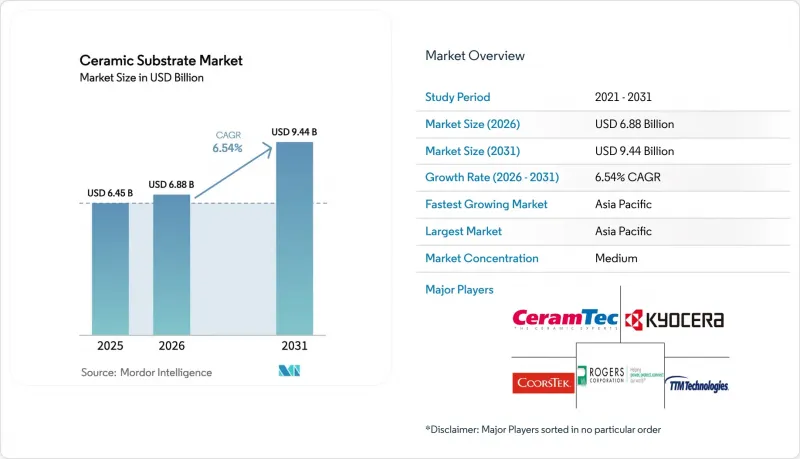
本報告按類型(氧化鋁、氮化鋁、氮化矽、氧化鈹等)、製造程序(高溫共燒陶瓷、低溫共燒陶瓷、直接塊狀陶瓷、陽極氧化鋁)、終端用戶行業(家用電子電器、汽車、半導體、電信等)和地區(亞太、北美、歐洲、南美、中東和非洲)進行細分。市場預測以美元計價。
全球陶瓷基板市場趨勢及洞察
優異的導熱性能,適用於實現高功率電子裝置。
如今,設計人員不再將導熱係數視為次要指標,而是視為首要限制。碳化矽 (SiC) MOSFET 和氮化鎵 (GaN) HEMT 的結溫高達 225 度C,產生的局部熱通量超過 300 W/cm²。這遠遠超過了環氧樹脂層壓板的安全限值。導熱係數為 170–250 W/m·K 的氮化鋁基基板可將散熱器體積減少 35%,並降低冷卻液流量,從而將系統整體效率提高 2–3%。直接接合銅 (DBC) 方法無需黏合層,可將熱阻降低 0.1 K·cm²/W,並使汽車牽引逆變器中的電流密度達到 200 A/cm²。此外,隨著多家公司投資將 SiC 晶圓直徑從 150 mm 增加到 200 mm,陶瓷基板市場預計將進一步擴張。
電動車逆變器和車載充電器的迅速普及導致了使用量的增加。
電池式電動車(BEV) 擴大採用 800V 架構,該架構會產生超過 1200V 的暫態電壓,並在 -40 度C至 150 度C的溫度範圍內承受高達 20 萬次的熱循環。為了滿足這些條件,汽車製造商正在採用 DBC基板,這種基板能夠承受足以損壞 FR-4基板的負載,並能承受毫秒的再生煞車極性反轉。氮化鋁基基板的碳化矽二極體可將車載充電器的效率提高到 98%,並透過將冷卻系統重量減輕 20% 來延長車輛續航里程。京瓷在長崎投資 4.54 億美元的擴建計畫將使其汽車基板產能在 2026 年底前翻倍。隨著模組成本的下降,高階市場的滲透率已超過 80%,主流市場的採用也正沿著成本下降的曲線推進,從而導致對陶瓷基板的強勁需求。
金屬和有機基板的高溢價
傳統材料的單價在每平方英吋 2 美元到 10 美元之間,而 FR-4 的成本僅為每平方英吋 0.10 美元到 0.50 美元,兩者相差 5 到 20 倍,這阻礙了其在許多消費性電子設備中的應用。氧化鋁粉末和金屬化製程佔總成本的 60%,良率降低又佔 15%,這意味著如果沒有製程創新,降價幾乎沒有下降空間。 2024 年至 2025 年的暫時性供不應求將導致價格上漲高達 20%,迫使一些行動電話製造商重新採用金屬芯 PCB。混合組件(僅在高熱通量元件下方使用陶瓷)可以在保持大部分散熱優勢的同時,將基板成本降低 30%。
細分市場分析
到2025年,氧化鋁將佔據陶瓷基板市場44.18%的佔有率,這主要得益於家用電子電器和工業驅動設備對成本的日益重視。同時,碳化矽基板的市場佔有率預計到2031年將以7.80%的複合年成長率成長,這主要得益於航太航太雷達和下一代電動車逆變器的應用,這些應用對熱膨脹係數的偏差必須控制在0.5 ppm/K以下。氮化鋁的熱導率為170–250 W/m*K,正擴大應用於800V級電動車平台,這些平台的結溫通常超過175 度C。
由於平均售價仍比氧化鋁同類產品高出3到5倍,這種高階材料的銷售成長前景良好。隨著相干公司(Coherent)、電裝公司(DENSO)和三菱電機公司投資10億美元建造200毫米碳化矽晶圓生產線,下游對相容基板的需求將加速成長,從而重塑陶瓷基板市場格局。預計到2031年,氧化鋁在LED和智慧型手機電源管理IC領域的銷售優勢仍將保持,但隨著通訊和資料中心設計人員轉向使用氮化鋁(AlN)以降低介電損耗,其市場佔有率將會下降。
區域分析
預計到2025年,亞太地區將佔全球銷售額的46.61%,並預計在2031年之前維持7.09%的複合年成長率。這主要得益於中國電動車產量在2024年突破900萬輛,以及日本計畫在2027年將其半透明氧化鋁晶片產能提高三倍。京瓷位於長崎的工廠計劃於2026年底竣工,該工廠將把碳化矽基板和先進封裝的生產線整合到同一地點,旨在縮短30%的前置作業時間,並增強區域自主生產能力。
預計到2025年,北美市場佔有率的擴張將主要得益於一項國防和航太計劃,該計劃指定相相位陣列鋁(AlN)基板,其工作溫度範圍為-55 度C至125 度C 。此外,《通貨膨脹控制法案》中針對清潔能源的激勵措施正在支持美國國內逆變器組裝,從而緩解了電動車普及速度較亞洲慢所帶來的影響。
在歐洲,能源價格飆升導致氧化鋁燒結成本較亞太地區上漲了25%。然而,歐盟的碳邊境調節機制(CBAM)將逐步徵收相當於每噸二氧化碳90美元的關稅,迫使原始設備製造商(OEM)轉向低碳氧化鋁,例如海德魯公司的「HalZero」氧化鋁,從而推動了該地區對可回收基板的需求。南美洲和中東及非洲地區的市佔率仍不到10%。巴西的太陽能帶和沙烏地阿拉伯的智慧城市「NEOM」等項目支撐著小眾需求,但對進口的高度依賴導致接收成本高出25%,限制了該地區陶瓷基板市場的擴張。
其他好處:
- Excel格式的市場預測(ME)表
- 3個月的分析師支持
目錄
第1章:引言
- 研究假設和市場定義
- 調查範圍
第2章:調查方法
第3章執行摘要
第4章 市場狀況
- 市場概覽
- 市場促進因素
- 優異的導熱性能推動了高功率電子設備對陶瓷基板的需求。
- 電動車逆變器和車載充電器的快速普及導致陶瓷基板的使用量增加。
- 高密度5G基地台和射頻模組
- 向SiC/GaN過渡需要AlN/DBC基板
- 低溫共燒陶瓷(LTCC)是航太領域立方衛星小型化的必要條件。
- 市場限制因素
- 與金屬/有機基板相比,價格溢價更高
- 組裝過程中的損壞和產量降低
- BeO毒性暴露限值
- 價值鏈分析
- 波特五力模型
第5章 市場規模與成長預測
- 按類型
- 氧化鋁
- 氮化鋁
- 氮化矽
- 氧化鈹
- 其他類型(科迪亞利特和碳化矽)
- 透過製造程序
- 高溫共燒陶瓷(HTCC)
- 低溫共燒陶瓷(LTCC)
- 直接接合銅(DBC)
- 活性金屬硬焊(AMB)
- 按最終用戶行業分類
- 家用電子產品
- 車
- 航太/國防
- 半導體
- 電訊
- 其他終端用戶產業(工業電力、可再生能源和醫療設備)
- 按地區
- 亞太地區
- 中國
- 印度
- 日本
- 韓國
- 越南
- 馬來西亞
- 印尼
- 泰國
- 其他亞太國家
- 北美洲
- 美國
- 加拿大
- 墨西哥
- 歐洲
- 德國
- 英國
- 法國
- 義大利
- 俄羅斯
- 土耳其
- 西班牙
- 北歐國家
- 其他歐洲國家
- 南美洲
- 巴西
- 阿根廷
- 哥倫比亞
- 其他南美國家
- 中東和非洲
- 沙烏地阿拉伯
- 南非
- 卡達
- 奈及利亞
- 阿拉伯聯合大公國
- 其他中東和非洲國家
- 亞太地區
第6章 競爭情勢
- 市場集中度
- 策略趨勢
- 市佔率和排名分析
- 公司簡介
- CeramTec GmbH
- CoorsTek Inc.
- Corning Incorporated
- Denka Company Limited
- Heraeus Electronics
- KOA Speer Electronic, Inc.
- KYOCERA Corporation
- LEATEC
- MARUWA Co., Ltd.
- NEOTech
- NIPPON CARBIDE INDUSTRIES CO., INC.
- Niterra Materials Co., Ltd.
- Ortech, Inc.
- Rogers Corporation
- TTM Technologies Inc.
- Yokowo Co., Ltd.
第7章 市場機會與未來展望
According to Mordor Intelligence, the ceramic substrate market size is projected to expand from USD 6.45 billion in 2025 and USD 6.88 billion in 2026 to USD 9.44 billion by 2031, registering a CAGR of 6.54% between 2026 to 2031.
This report is Segmented by Type (Alumina, Aluminum Nitride, Silicon Nitride, Beryllium Oxide, and More), Manufacturing Process (HTCC, LTCC, DBC, and AMB), End-User Industry (Consumer Electronics, Automotive, Semiconductor, Telecommunications, and More), and Geography (Asia-Pacific, North America, Europe, South America, and Middle East and Africa). Market Forecasts are Provided in Terms of Value (USD).
Global Ceramic Substrate Market Trends and Insights
Superior Thermal Conductivity Enabling High-Power Electronics
Designers now treat thermal conductivity as a primary constraint rather than a secondary specification. Silicon-carbide MOSFETs and gallium-nitride HEMTs run at junction temperatures up to 225°C, generating local heat fluxes that top 300 W/cm2, well beyond the safe envelope for epoxy-based laminates. Aluminum-nitride substrates, offering 170-250 W/m*K, cut heat-sink volume by 35% and trim liquid-coolant flow rates, improving full-system efficiency by 2-3%. Direct-bonded-copper (DBC) variants eliminate adhesive layers, slicing thermal resistance by 0.1 K*cm2/W and allowing current densities of 200 A/cm2 in automotive traction inverters. Multi-company investments that will lift global SiC wafer output from 150-mm to 200-mm diameters further expand the ceramic substrate market.
Rapid EV Inverter and On-Board-Charger Build-Out Increasing Usage
Battery-electric vehicles are standardizing on 800-V architectures, which impose voltage transients above 1,200 V and thermal cycling from -40°C to 150°C over 200,000 cycles. To meet these conditions, automakers integrate DBC substrates that handle regenerative-braking reversals within milliseconds, loads that fracture FR-4 boards. Silicon-carbide diodes on aluminum-nitride bases lift on-board-charger efficiency to 98% and shave cooling-system mass by 20%, extending vehicle range. Kyocera's USD 454 million Nagasaki build-out will double automotive-grade substrate capacity by late 2026. As module costs fall, premium-segment penetration already exceeds 80%, and mainstream adoption is tracking downward cost curves, cementing demand for the ceramic substrate market.
High Price Premium Over Metal/Organic Boards
Unit prices range from USD 2 to USD 10 per square inch versus USD 0.10-0.50 for FR-4, a 5-to-20-fold spread that shuts entry into many consumer devices. Raw alumina powder and metallization account for 60% of the cost, while yield loss contributes another 15%, leaving scant room for markdowns without process innovation. Temporary shortages in 2024-2025 inflated prices by up to 20%, compelling some handset makers to revert to metal-core PCBs. Hybrid assemblies that place ceramic only under high-heat-flux components cut substrate spend by 30% while retaining most thermal benefit.
Other drivers and restraints analyzed in the detailed report include:
- 5G Base-Station and RF Module Densification
- SiC/GaN Migration Requiring AlN and DBC Substrates
- Fragility and Yield Losses During Assembly
For complete list of drivers and restraints, kindly check the Table Of Contents.
Segment Analysis
Alumina delivered 44.18% of the ceramic substrate market share in 2025, anchored by cost-sensitive consumer electronics and industrial drives. At the same time, silicon carbide substrates expanded 7.80% CAGR through 2031, propelled by aerospace radars and next-generation EV inverters that require coefficient-of-thermal-expansion mismatches below 0.5 ppm/K. Aluminum nitride, with 170-250 W/m*K conductivity, is gaining traction in 800-V EV platforms where operating junctions exceed 175°C.
Revenue momentum favors premium materials because average selling prices remain three to five times higher than alumina equivalents. As Coherent, DENSO, and Mitsubishi Electric pour USD 1 billion into 200-mm SiC wafer lines, downstream demand for compatible substrates will accelerate, reshaping the ceramic substrate market size profile. Alumina will keep its volume edge through 2031 in LEDs and smartphone power-management ICs, yet its revenue share will slip as telecom and data-center designers upgrade to AlN for lower dielectric loss.
Complete Report Scope:
- By Type
- Alumina
- Aluminum Nitride
- Silicon Nitride
- Beryllium Oxide
- Other Types (Cordierite andSilicon Carbide)
- By Manufacturing Process
- High-Temperature Co-Fired Ceramic (HTCC)
- Low-Temperature Co-Fired Ceramic (LTCC)
- Direct Bonded Copper (DBC)
- Active Metal Brazed (AMB)
- By End-User Industry
- Consumer Electronics
- Automotive
- Aerospace & Defense
- Semiconductor
- Telecommunications
- Other End-user Industries (Industrial Power & Renewable Energy, and Medical Devices)
- By Geography
- Asia-Pacific
- China
- India
- Japan
- South Korea
- Vietnam
- Malaysia
- Indonesia
- Thailand
- Rest of Asia-Pacific
- North America
- United States
- Canada
- Mexico
- Europe
- Germany
- United Kingdom
- France
- Italy
- Russia
- Turkey
- Spain
- NORDIC Countries
- Rest of Europe
- South America
- Brazil
- Argentina
- Colombia
- Rest of South America
- Middle East and Africa
- Saudi Arabia
- South Africa
- Qatar
- Nigeria
- United Arab Emirates
- Rest of Middle East and Africa
- Asia-Pacific
Geography Analysis
Asia-Pacific contributed 46.61% of revenue in 2025 and is expected to post a 7.09% CAGR through 2031, buoyed by Chinese EV output topping 9 million units in 2024 and Japanese initiatives to triple translucent-alumina wafer capacity by fiscal 2027. Kyocera's Nagasaki complex, slated for late 2026 completion, will co-locate SiC substrate and advanced packaging lines, cutting lead times by 30% and reinforcing regional self-sufficiency.
North America's 2025 share was driven by defense and space programs that specify AlN substrates for phased-array radars operating across -55°C to 125°C. The Inflation Reduction Act's clean-energy incentives underpin domestic inverter assembly, cushioning slower EV penetration relative to Asia.
In Europe, high energy prices inflate alumina sintering costs by 25% versus Asia-Pacific, but the EU Carbon Border Adjustment Mechanism, phasing in USD 90-equivalent tariffs per ton of CO2, nudges OEMs toward low-carbon alumina such as Hydro's HalZero, lifting regional demand for recyclable substrates. South America and the Middle East & Africa remain sub-10% contributors; projects in Brazil's solar belt and Saudi Arabia's NEOM smart-city keep niche demand alive, yet import reliance raises landed cost by up to 25%, limiting the ceramic substrate market's expansion there.
- CeramTec GmbH
- CoorsTek Inc.
- Corning Incorporated
- Denka Company Limited
- Heraeus Electronics
- KOA Speer Electronic, Inc.
- KYOCERA Corporation
- LEATEC
- MARUWA Co., Ltd.
- NEOTech
- NIPPON CARBIDE INDUSTRIES CO., INC.
- Niterra Materials Co., Ltd.
- Ortech, Inc.
- Rogers Corporation
- TTM Technologies Inc.
- Yokowo Co., Ltd.
Additional Benefits:
- The market estimate (ME) sheet in Excel format
- 3 months of analyst support
TABLE OF CONTENTS
1 Introduction
- 1.1 Study Assumptions & Market Definition
- 1.2 Scope of the Study
2 Research Methodology
3 Executive Summary
4 Market Landscape
- 4.1 Market Overview
- 4.2 Market Drivers
- 4.2.1 Superior thermal conductivity driving the demand for ceramic substrates in high-power electronics
- 4.2.2 Rapid EV inverter & on-board-charger build-out increasing ceramic substarte usage
- 4.2.3 5G base-station and RF module densification
- 4.2.4 SiC/GaN migration requiring AlN & DBC substrates
- 4.2.5 Aerospace CubeSat miniaturisation needs LTCC
- 4.3 Market Restraints
- 4.3.1 High price premium over metal/organic boards
- 4.3.2 Fragility & yield losses during assembly
- 4.3.3 Toxic-exposure limits on BeO
- 4.4 Value Chain Analysis
- 4.5 Porter's Five Forces
- 4.5.1 Threat of New Entrants
- 4.5.2 Bargaining Power of Suppliers
- 4.5.3 Bargaining Power of Buyers
- 4.5.4 Threat of Substitutes
- 4.5.5 Degree of Competition
5 Market Size & Growth Forecasts (Value)
- 5.1 By Type
- 5.1.1 Alumina
- 5.1.2 Aluminum Nitride
- 5.1.3 Silicon Nitride
- 5.1.4 Beryllium Oxide
- 5.1.5 Other Types (Cordierite andSilicon Carbide)
- 5.2 By Manufacturing Process
- 5.2.1 High-Temperature Co-Fired Ceramic (HTCC)
- 5.2.2 Low-Temperature Co-Fired Ceramic (LTCC)
- 5.2.3 Direct Bonded Copper (DBC)
- 5.2.4 Active Metal Brazed (AMB)
- 5.3 By End-User Industry
- 5.3.1 Consumer Electronics
- 5.3.2 Automotive
- 5.3.3 Aerospace & Defense
- 5.3.4 Semiconductor
- 5.3.5 Telecommunications
- 5.3.6 Other End-user Industries (Industrial Power & Renewable Energy, and Medical Devices)
- 5.4 By Geography
- 5.4.1 Asia-Pacific
- 5.4.1.1 China
- 5.4.1.2 India
- 5.4.1.3 Japan
- 5.4.1.4 South Korea
- 5.4.1.5 Vietnam
- 5.4.1.6 Malaysia
- 5.4.1.7 Indonesia
- 5.4.1.8 Thailand
- 5.4.1.9 Rest of Asia-Pacific
- 5.4.2 North America
- 5.4.2.1 United States
- 5.4.2.2 Canada
- 5.4.2.3 Mexico
- 5.4.3 Europe
- 5.4.3.1 Germany
- 5.4.3.2 United Kingdom
- 5.4.3.3 France
- 5.4.3.4 Italy
- 5.4.3.5 Russia
- 5.4.3.6 Turkey
- 5.4.3.7 Spain
- 5.4.3.8 NORDIC Countries
- 5.4.3.9 Rest of Europe
- 5.4.4 South America
- 5.4.4.1 Brazil
- 5.4.4.2 Argentina
- 5.4.4.3 Colombia
- 5.4.4.4 Rest of South America
- 5.4.5 Middle East and Africa
- 5.4.5.1 Saudi Arabia
- 5.4.5.2 South Africa
- 5.4.5.3 Qatar
- 5.4.5.4 Nigeria
- 5.4.5.5 United Arab Emirates
- 5.4.5.6 Rest of Middle East and Africa
- 5.4.1 Asia-Pacific
6 Competitive Landscape
- 6.1 Market Concentration
- 6.2 Strategic Moves
- 6.3 Market Share(%)/Ranking Analysis
- 6.4 Company Profiles (includes Global level Overview, Market level overview, Core Segments, Financials as available, Strategic Information, Market Rank/Share for key companies, Products & Services, and Recent Developments)
- 6.4.1 CeramTec GmbH
- 6.4.2 CoorsTek Inc.
- 6.4.3 Corning Incorporated
- 6.4.4 Denka Company Limited
- 6.4.5 Heraeus Electronics
- 6.4.6 KOA Speer Electronic, Inc.
- 6.4.7 KYOCERA Corporation
- 6.4.8 LEATEC
- 6.4.9 MARUWA Co., Ltd.
- 6.4.10 NEOTech
- 6.4.11 NIPPON CARBIDE INDUSTRIES CO., INC.
- 6.4.12 Niterra Materials Co., Ltd.
- 6.4.13 Ortech, Inc.
- 6.4.14 Rogers Corporation
- 6.4.15 TTM Technologies Inc.
- 6.4.16 Yokowo Co., Ltd.
7 Market Opportunities & Future Outlook
- 7.1 White-space & Unmet-Need Assessment
- 7.2 CBAM pushes EU OEMs to recyclable alumina

 陶瓷基板市場:按產品類型、材料類型、製造流程、形狀、厚度、應用和銷售管道分類-全球市場預測(2026-2032 年)
 陶瓷基板市場規模、佔有率及成長分析:依材料化學成分、功能製造技術、主要應用領域、終端用戶產業及地區分類-2026-2033年產業預測
 全球陶瓷基板市場規模、佔有率、趨勢及成長分析報告(2026-2034年)
 2026年全球電子封裝陶瓷基板市場報告
 2025-2029年全球陶瓷基板市場全球燒結釬焊膏市場(按成分、包裝類型、應用、終端用戶產業和分銷管道分類)預測(2026-2032年)
 陶瓷基板市場規模、佔有率和趨勢分析報告:按產品、最終用途、地區和細分市場預測(2025-2033 年)
 DBC陶瓷基板:全球市佔率及排名、總收入及需求預測(2025-2031年)DCB 和 AMB基板:2025-2031 年全球市場佔有率和排名、總收入和需求預測SiN AMB基板:全球市場佔有率和排名、總收入和需求預測(2025-2031年)