

 |
市場調查報告書
商品編碼
2113967
物理氣相澱積(PVD)設備:市場佔有率分析、產業趨勢與統計、成長預測(2026-2031)Physical Vapor Deposition (PVD) Equipment - Market Share Analysis, Industry Trends & Statistics, Growth Forecasts (2026 - 2031) |
||||||

※ 本網頁內容可能與最新版本有所差異。詳細情況請與我們聯繫。
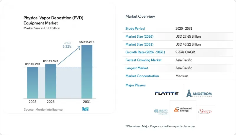
據 Mordor Intelligence 稱,物理氣相澱積(PVD) 設備的市場規模預計在 2026 年達到 276.5 億美元,高於 2025 年的 252.9 億美元,預計到 2031 年將達到 432.2 億美元。
預計從 2026 年到 2031 年,其複合年成長率將達到 9.33%。
本報告依沉積技術(陰極電弧沉積、電子束物理氣相沉積等)、終端用戶(微電子、醫療設備等)、基板(金屬、塑膠等)、薄膜厚度(小於1微米、1-3微米等)及地區進行細分。市場預測以美元計價。
全球物理氣相澱積(PVD)設備市場趨勢及洞察
對先進微電子技術和半導體小型化的需求日益成長。
向2奈米環柵(GaA)電晶體的節點過渡需要採用高通量磁控濺鍍器沉積超薄氮化鉭功函數層,這推動了台灣、韓國和美國對多腔室濺射設備的需求。一座月產4萬片晶圓的新晶圓廠需要25到30個濺射腔室,用於銅阻擋層、種子層和覆蓋層製程。叢集整合技術將預清洗、沉積和退火製程整合於單一真空腔內,可將顆粒缺陷減少30%,目前已成為3奈米製程量產的事實標準。先進封裝技術也進一步推動了對銅的需求,因為混合鍵結晶片和穿透矽通孔(TSV)需要將銅的厚度從500奈米重新分佈到2微米。
記憶體製造商正在認證PVD鎢用於300層3D NAND閃存,理由是其相比化學氣相沉積法(CVD)能實現更精確的層厚控制。更重要的是,鼓勵採購國產設備的區域性補貼政策提升了區域供應商的地位,並將最先進的晶圓廠採購週期從四年縮短至三年。
政府對國內半導體製造設備的獎勵措施
美國《晶片與科學法案》提供390億美元的製造津貼和110億美元的貸款,並規定30%的資本投資必須來自美國供應商。光是英特爾一家就已為其位於亞利桑那州、俄亥俄州和新墨西哥州的生產線購置了200多台PVD工藝室。歐洲的《晶片法案》總額達430億歐元(約477億美元),其中300億歐元(約333億美元)已投資於英特爾位於馬德堡的工廠,並支持台積電在德勒斯登的合資企業。該法案同樣包含在地採購條款,增加了來自Veeco、Oerlikon和Von Ardenne等公司的訂單。日本、韓國和中國也設有類似的補貼計劃,要麼補貼40%的資本投資,要麼為進口設備提供多年免稅優惠,從而有效地將投資回收期縮短至五年以內。
隨著新晶圓廠投入運作,PVD 設備市場在三大洲的需求同步成長,儘管半導體產業的經濟週期出現下滑,但累積訂單正在趨於穩定。
巨額資本投資
用於300毫米晶圓的先進磁控濺鍍叢集造價在300萬至500萬美元之間,但一條完整的邏輯生產線通常包含20至30個腔室,這意味著初始認證前的投資超過1億美元。服務合約、備件包和耗材靶材成本也會使總成本增加15%至20%。對於以切割刀具和裝飾市場為導向的小規模塗層公司而言,每台陰極電弧濺鍍裝置的購置價格為50萬至80萬美元,需要1萬至1.5萬個處理週期才能達到損益平衡點。
租賃和晶圓收費模式將進入門檻降低了40%,但同時也把運轉率的風險轉移給了投資方,並使每個組件的成本增加了約10%。因此,新參與企業傾向於採用模組化、單室設計,而大型叢集在Tier 1晶圓廠以外的應用仍然有限。
細分市場分析
磁控濺鍍在2025年佔了57.68%的銷售額。這是因為其低能離子轟擊技術能夠沉積晶圓上異質性小於2%的銅和鉭薄膜。這是300毫米後端製程(BEOL)所允許的最低公差。受邏輯晶片和3D NAND晶片產量成長的推動,採用磁控濺射的物理氣相澱積(PVD)設備的市場規模預計將以8.42%的複合年成長率成長。這些晶片每個金屬化迴路需要6到8個腔室。離子鍍目前市佔率不足15%,但預計到2031年將以10.72%的年均成長率成長,因為切削刀具和裝飾五金製造商正在加大對高密度柱狀薄膜的投資,這種薄膜在附著力和耐腐蝕性方面優於電鍍鉻。在降低整體擁有成本 (TCO) 方面,旋轉陰極和封閉回路型等離子體監測器具有優勢,可將靶材壽命延長 50%,並將廢品率降低至 3% 以下。陰極電弧和電子束 PVD 仍屬於小眾應用,主要用於對顆粒污染和聚合物收縮要求極高的應用和低溫光學元件,在這些應用中,顆粒污染和聚合物收縮是關鍵問題。由於 SEMI 標準與技術選擇無關,買家優先考慮的是產量、耗材和運作,這進一步強化了磁控管的優勢,同時也為滿足新興的軟性電子產品需求而採用專門方法留下了空間。
目前,離子鍍供應商正在銷售可在高功率脈衝濺鍍和直流輝光濺鍍之間切換的混合腔室,從而實現鈦鋁氮化物、氮化鋯和類金剛石碳的連續循環沉積。這種柔軟性可將因清潔造成的停機時間減少一半,並提高塗層中心的占地面積效益。同時,應用材料公司(Applied Materials)的14工位「Endura」叢集將客戶與其自身的預清洗、阻隔層、晶種和封層製程配方綁定在一起,這種生態系統確保了耗材的持續採購,從而推高了轉換成本。因此,在物理氣相澱積(PVD)設備市場,整合平台的深度仍備受重視,而單腔室系統的移動性也依然重要。
預計到2025年,微電子產業將佔銷售額的42.05%,因為代工廠依賴PVD技術來製備銅雙大馬士革紋、氮化鉭阻擋層和鋁焊墊。假設製程節點轉移和混合鍵合晶片維持目前的資本投資趨勢,到2031年,微電子PVD設備市場規模可能超過266億美元。同時,切削刀具產業成長最快,複合年成長率達11.28%,因為航太和汽車業的加工方式正轉向乾式高速加工方法,而鈦鋁氮化物三層層級構造可以延長刀具壽命。墨西哥、印度和東歐離子鍍設施的部署凸顯了金屬切割供應鏈的地理重組。醫療設備約佔市場佔有率的14%,根據FDA 510(k)申請,光是2024年就有超過40種PVD塗層整形外科植入獲得核准。雖然太陽能電池產品目前佔銷售額的 11%,但俄亥俄州、馬來西亞和古吉拉突邦產能的提高意味著,到 2028 年,薄膜太陽能電池的成長速度預計將超過全球平均組件成長率。
監管流程的差異導致不同終端使用者的實施時間表各不相同。醫療植入每種新塗層都需要18-24個月的生物相容性測試,而半導體採購決策則集中在節點發布前後6-9個月內。切削刀具服務的認證要求極低,使得製造製程配方能夠在數週內實現商業化。因此,收入多元化有助於穩定PVD設備市場的整體成長,並減輕矽晶圓廠造成的經濟波動的影響。
區域分析
預計到2025年,亞太地區將佔全球銷售額的37.88%,這主要得益於台積電(TSMC)多年1650億美元的投資、三星晶圓代工平澤和華城工廠的擴建,以及中國力爭在2010年底前實現設備70%自給率的目標。日本經濟產業省(METI)的補貼計畫可報銷高達40%的符合條件的資本投資,使ULVAC和東京電子等公司能夠加快濺射腔組件的在地化生產,並縮短前置作業時間。印度100億美元的半導體激勵計畫已批准三個300毫米晶圓廠項目,每個項目預計將安裝25-30個PVD濺射腔,預計到2028年將使設備訂單增加5億美元。
截至2025年,北美市佔率為27.74%。 《晶片技術創新法案》(CHIPS Act)為英特爾、台積電、三星和美光提供了資金支持,每家公司都制定了各自的美國境內供應需求,這有利於美國濺射室和靶材製造廠的發展。光是英特爾位於俄亥俄州的園區就計畫安裝200多台PVD設備,用於18A和14A製程的生產,代表著10億美元的商機。美光位於紐約的高頻寬記憶體製造地使用鎢和銅濺射模組生產垂直堆疊式DRAM,而其位於加拿大的化合物半導體叢集正在投資電子束PVD設備,用於生產氮化鎵射頻裝置。
預計到2025年底,歐洲將佔據21.86%的市場。歐盟已撥款430億歐元(約477億美元)用於激勵措施,以支持英特爾馬德堡工廠、台積電德勒斯登工廠和意法半導體等公司拓展碳化矽(SiC)業務。德國的國內採購稅率規定了30%的最低本地增值率,這對Auricon、Vico和Von Ardennes等公司來說是一大利好。法國耗資5億歐元(約5.55億美元)的先進封裝工程新增了用於銅重分佈和混合鍵結的濺鍍迴路試驗裝置。該地區嚴格的等離子體排放法規有利於採用內置氟氣去除功能的設備,從而鞏固了符合環保要求的供應商的競爭優勢。
其他好處:
- Excel格式的市場預測(ME)表
- 3個月的分析師支持
目錄
第1章:引言
- 研究假設和市場定義
- 調查範圍
第2章:調查方法
第3章執行摘要
第4章 市場狀況
- 市場概覽
- 價值鏈分析
- 宏觀經濟因素對市場的影響
- 市場促進因素
- 對先進微電子產品的需求不斷成長以及半導體的微型化
- 需要生物相容性塗層的高性能醫療植入的發展
- 薄膜太陽能電池組件的廣泛應用
- 政府對境內半導體製造設備的獎勵措施
- 電動車傳動系統零件對耐磨塗層的需求
- 將PVD技術整合到軟性電子產品製造中
- 市場限制因素
- 巨額資本投資
- 透過 ALD 和 CVD 等替代薄膜沉積技術展開競爭。
- 高純度靶材供應鏈中的脆弱性
- 嚴格的等離子體排放環境法規
- 監理情勢
- 技術展望
- 波特五力分析
第5章 市場規模與成長預測
- 透過沉澱技術
- 陰極電弧沉積
- 電子束物理氣相沉積
- 磁控濺射
- 離子鍍
- 其他沉積技術
- 最終用戶
- 微電子學
- 醫療器材與設備
- 太陽能產品
- 切削刀具
- 其他最終用戶
- 按基板
- 金屬
- 塑膠
- 玻璃
- 陶瓷
- 其他基板
- 按塗層厚度
- 小於1微米
- 1-3微米
- 3-5微米
- 5微米或以上
- 按地區
- 北美洲
- 美國
- 加拿大
- 墨西哥
- 歐洲
- 德國
- 法國
- 英國
- 義大利
- 西班牙
- 其他歐洲國家
- 亞太地區
- 中國
- 日本
- 韓國
- 印度
- 其他亞太國家
- 中東
- 沙烏地阿拉伯
- 阿拉伯聯合大公國
- 土耳其
- 其他中東國家
- 非洲
- 南非
- 奈及利亞
- 其他非洲國家
- 南美洲
- 巴西
- 阿根廷
- 其他南美國家
- 北美洲
第6章 競爭情勢
- 市場集中度
- 策略趨勢
- 市佔率分析
- 公司簡介
- Advanced Energy Industries Inc.
- Angstrom Engineering Inc.
- Veeco Instruments Inc.
- Applied Materials Inc.
- Platit AG
- Mustang Vacuum Systems LLC
- Oerlikon Balzers Coating AG
- ULVAC Inc.
- Semicore Equipment Inc.
- AJA International Inc.
- IHI Corporation
- Shincron Co. Ltd.
- Kolzer Srl
- BCI Blosch AG
- Denton Vacuum LLC
- Buhler AG
- Intevac Inc.
- Kurt J. Lesker Company
- Kobelco Sputtering Systems Corp.
- Picosun Oy
第7章 投資分析
第8章 市場機會與未來展望
- 評估尚未開發的市場和未滿足的需求
According to Mordor Intelligence, physical vapor deposition equipment market size in 2026 is estimated at USD 27.65 billion, growing from 2025 value of USD 25.29 billion with 2031 projections showing USD 43.22 billion, growing at 9.33% CAGR over 2026-2031.
This report is Segmented by Deposition Technique (Cathodic Arc Deposition, Electron Beam PVD, and More), End User (Microelectronics, Medical Devices and Equipment, and More), Substrate Material (Metals, Plastics, and More), Coating Thickness (Below 1 Micron, 1-3 Micron, and More), and Geography. The Market Forecasts are Provided in Terms of Value (USD).
Global Physical Vapor Deposition (PVD) Equipment Market Trends and Insights
Rising Demand for Advanced Microelectronics and Semiconductor Scaling
Node migration to 2-nanometer gate-all-around transistors requires ultra-thin tantalum-nitride work-function layers deposited by magnetron sputtering at high throughput, driving multi-chamber demand in Taiwan, South Korea, and the United States. Every new 40,000 wafer-per-month fab needs 25-30 sputter chambers for copper barrier, seed, and capping steps. Cluster integration that combines pre-clean, deposition, and anneal inside one vacuum envelope cuts particulate defects by 30% and is now a de-facto specification in 3 nanometre ramps. Advanced packaging adds further pull, because hybrid-bonded chiplets and through-silicon vias require copper redistribution at 500 nanometers to 2 microns.
Memory producers are qualifying PVD tungsten for 300-layer 3D NAND, citing tighter step-coverage control than chemical vapor routes. Most importantly, local subsidies that favour domestic tool sourcing elevate regional suppliers and shorten purchasing cycles from four to three years in leading-edge fabs.
Government Incentives for Onshore Semiconductor Equipment Manufacturing
The United States CHIPS and Science Act released USD 39 billion in manufacturing grants and USD 11 billion in loans, stipulating that 30% of equipment spend must originate from U.S. vendors. Intel alone earmarked more than 200 PVD chambers for Arizona, Ohio, and New Mexico lines. Europe's EUR 43 billion (USD 47.7 billion) Chips Act channels EUR 30 billion (USD 33.3 billion) into Intel Magdeburg and supports TSMC's Dresden joint venture, again with local-content clauses that lift orders for Veeco, Oerlikon, and Von Ardenne. Japan, South Korea, and China run parallel subsidy programs that either cover 40% of capex or offer multi-year tax holidays on imported equipment, effectively lowering payback periods below five years.
As new fabs come online, the PVD equipment market enjoys synchronized demand in three continents, stabilizing order books against cyclical semiconductor downturns.
High Capital Investment
A state-of-the-art magnetron sputtering cluster for 300-millimeter wafers costs USD 3-5 million, while fully configured logic lines often install 20-30 chambers, pushing upfront outlays above USD 100 million before qualification. Service contracts, spare kits, and consumable targets add a further 15-20% to lifetime ownership. Smaller coaters in cutting-tool or decorative markets face USD 0.5-0.8 million ticket prices per cathodic-arc tool and must process 10,000-15,000 cycles to break even.
Although leasing and pay-per-wafer models lower entry barriers by 40%, they transfer utilization risk to financiers and raise per-part cost by roughly 10%. Consequently, new entrants gravitate toward modular single-chamber designs, limiting large-cluster penetration outside tier-one fabs.
Other drivers and restraints analyzed in the detailed report include:
- Increasing Adoption of Thin-Film Solar Modules
- Demand for Wear-Resistant Coatings in Electric Vehicle Drivetrain Components
- Competition from Alternative Deposition Technologies Such as ALD and CVD
For complete list of drivers and restraints, kindly check the Table Of Contents.
Segment Analysis
Magnetron sputtering delivered 57.68% of 2025 revenue because its low-energy ion bombardment spreads copper and tantalum films with <2% across-wafer non-uniformity, the tightest window tolerated in 300-millimeter back-end-of-line runs. The physical vapor deposition (PVD) equipment market size for magnetron tools is projected to rise at 8.42% CAGR, reinforced by logic and 3D NAND ramps that each consume 6-8 chambers per metallization loop. Ion plating, although currently below 15% share, is forecast to progress at 10.72% through 2031 as cutting-tool and decorative-hardware producers invest in dense columnar films that outperform electroplated chrome on adhesion and corrosion. Cost-of-ownership gains favour rotary cathodes and closed-loop plasma monitors that extend target life by 50% and slash scrap below 3%. Cathodic-arc and electron-beam PVD stay niche, serving extreme-hardness or low-temperature optics where particle contamination or polymer shrinkage is mission-critical. With SEMI standards agnostic to technique selection, buyers weigh throughput, consumables, and uptime, reinforcing magnetron dominance yet leaving whitespace for specialized approaches that address emerging flexible-electronics demands.
Ion-plating vendors now market hybrid chambers that flip between high-power impulse sputtering and DC glow to accommodate titanium-aluminium-nitride, zirconium-nitride, and diamond-like carbon in consecutive cycles. Such flexibility halves cleaning downtime and boosts revenue per floor area in coating centers. Meanwhile, Applied Materials' fourteen-station Endura cluster locks customers into proprietary pre-clean, barrier, seed, and cap recipes, an ecosystem that secures pull-through consumables and inflates switching costs. Consequently, the physical vapor deposition (PVD) equipment market continues to reward integrated platform depth on one end and nimble single-chamber agility on the other.
Microelectronics secured 42.05% of 2025 turnover because foundries rely on PVD for copper dual-damascene, tantalum-nitride barriers, and aluminium bond pads. The PVD equipment market size for microelectronics could pass USD 26.6 billion by 2031, assuming node migrations and hybrid-bonded chiplets maintain current capex vectors. Cutting tools, however, are pacing fastest at 11.28% CAGR as aerospace and automotive machining shifts toward dry, high-speed protocols where titanium-aluminium-nitride triples insert life. Ion-plating site rollouts in Mexico, India, and Eastern Europe highlight geographic realignment of metal-cutting supply chains. Medical devices hold roughly 14% share, with FDA 510(k) filings showing over forty PVD-coated orthopaedics implants cleared in 2024 alone. Solar products contribute 11% of revenue, yet capacity expansions in Ohio, Malaysia, and Gujarat position thin-film PV to outgrow global module averages through 2028.
Regulatory processes shape adoption timelines differently across end users. Medical implants require 18-24 months of biocompatibility testing per new coating, while semiconductor purchase decisions compress into 6-9-month windows around node releases. Cutting-tool services face minimal accreditation and can commercialize recipes within weeks. As a result, revenue diversity stabilizes aggregate growth for the PVD equipment market, cushioning cyclical swings tied to silicon fabs.
Complete Report Scope:
- By Deposition Technique
- Cathodic Arc Deposition
- Electron Beam PVD
- Magnetron Sputtering
- Ion Plating
- Other Deposition Techniques
- By End User
- Microelectronics
- Medical Devices and Equipment
- Solar Products
- Cutting Tools
- Other End Users
- By Substrate Material
- Metals
- Plastics
- Glass
- Ceramics
- Others Substrate Material
- By Coating Thickness
- Below 1 Micron
- 1 - 3 Micron
- 3 - 5 Micron
- Above 5 Micron
- By Geography
- North America
- United States
- Canada
- Mexico
- Europe
- Germany
- France
- United Kingdom
- Italy
- Spain
- Rest of Europe
- Asia Pacific
- China
- Japan
- South Korea
- India
- Rest of Asia Pacific
- Middle East
- Saudi Arabia
- United Arab Emirates
- Turkey
- Rest of Middle East
- Africa
- South Africa
- Nigeria
- Rest of Africa
- South America
- Brazil
- Argentina
- Rest of South America
- North America
Geography Analysis
Asia Pacific commanded 37.88% of 2025 sales and is positioned to log a 9.97% CAGR through 2031, underpinned by Taiwan Semiconductor Manufacturing Company's USD 165 billion multiyear spend, Samsung Foundry's Pyeongtaek and Hwaseong expansions, and the People's Republic of China's goal of 70% equipment self-reliance by decade-end. Japan's METI subsidies reimburse up to 40% of qualifying capex, encouraging ULVAC and Tokyo Electron to localize sputter chamber components and shorten lead times. India's USD 10 billion chip incentive accepted three 300-millimeter fab proposals, each projecting 25-30 PVD chambers and potentially adding USD 500 million in tool orders by 2028.
North America held 27.74% share in 2025. The CHIPS Act funded Intel, TSMC, Samsung, and Micron, each stipulating domestic supply requirements that favour U.S. chamber and target plants. Intel's Ohio campus alone plans over 200 PVD tools for 18A and 14A production, representing a USD 1 billion opportunity. Micron's high-bandwidth-memory site in New York will consume tungsten and copper sputter modules for vertical DRAM stacks, while Canada's compound-semiconductor cluster invests in electron-beam PVD for gallium-nitride RF devices.
Europe finished 2025 at 21.86% share. The European Union converted EUR 43 billion (USD 47.7 billion) of incentives into Intel Magdeburg, TSMC Dresden, and STMicroelectronics silicon-carbide expansions. German onshore-content rules define a 30% local-value floor, creating tailwinds for Oerlikon, Veeco, and Von Ardenne. France's EUR 500 million (USD 555 million) advanced-packaging program adds pilot sputter loops for copper redistribution and hybrid bonding. Strict plasma-emission mandates in the region favour tools with built-in fluorinated-gas abatement, cementing competitive advantage for suppliers that bundle environmental compliance.
- Advanced Energy Industries Inc.
- Angstrom Engineering Inc.
- Veeco Instruments Inc.
- Applied Materials Inc.
- Platit AG
- Mustang Vacuum Systems LLC
- Oerlikon Balzers Coating AG
- ULVAC Inc.
- Semicore Equipment Inc.
- AJA International Inc.
- IHI Corporation
- Shincron Co. Ltd.
- Kolzer Srl
- BCI Blosch AG
- Denton Vacuum LLC
- Buhler AG
- Intevac Inc.
- Kurt J. Lesker Company
- Kobelco Sputtering Systems Corp.
- Picosun Oy
Additional Benefits:
- The market estimate (ME) sheet in Excel format
- 3 months of analyst support
TABLE OF CONTENTS
1 INTRODUCTION
- 1.1 Study Assumptions and Market Definition
- 1.2 Scope of the Study
2 RESEARCH METHODOLOGY
3 EXECUTIVE SUMMARY
4 MARKET LANDSCAPE
- 4.1 Market Overview
- 4.2 Value-Chain Analysis
- 4.3 Impact of Macroeconomic Factors on the Market
- 4.4 Market Drivers
- 4.4.1 Rising Demand for Advanced Microelectronics and Semiconductor Scaling
- 4.4.2 Growth of High-Performance Medical Implants Requiring Biocompatible Coatings
- 4.4.3 Increasing Adoption of Thin-Film Solar Modules
- 4.4.4 Government Incentives for Onshore Semiconductor Equipment Manufacturing
- 4.4.5 Demand for Wear-Resistant Coatings in Electric Vehicle Drivetrain Components
- 4.4.6 Integration of PVD in Flexible Electronics Manufacturing
- 4.5 Market Restraints
- 4.5.1 High Capital Investment
- 4.5.2 Competition from Alternative Deposition Technologies such as ALD and CVD
- 4.5.3 Supply Chain Vulnerabilities for High-Purity Target Materials
- 4.5.4 Stringent Environmental Regulations on Plasma Emissions
- 4.6 Regulatory Landscape
- 4.7 Technological Outlook
- 4.8 Porter's Five Forces Analysis
- 4.8.1 Bargaining Power of Suppliers
- 4.8.2 Bargaining Power of Buyers
- 4.8.3 Threat of New Entrants
- 4.8.4 Intensity of Competitive Rivalry
- 4.8.5 Threat of Substitute Products
5 MARKET SIZE AND GROWTH FORECASTS (VALUE)
- 5.1 By Deposition Technique
- 5.1.1 Cathodic Arc Deposition
- 5.1.2 Electron Beam PVD
- 5.1.3 Magnetron Sputtering
- 5.1.4 Ion Plating
- 5.1.5 Other Deposition Techniques
- 5.2 By End User
- 5.2.1 Microelectronics
- 5.2.2 Medical Devices and Equipment
- 5.2.3 Solar Products
- 5.2.4 Cutting Tools
- 5.2.5 Other End Users
- 5.3 By Substrate Material
- 5.3.1 Metals
- 5.3.2 Plastics
- 5.3.3 Glass
- 5.3.4 Ceramics
- 5.3.5 Others Substrate Material
- 5.4 By Coating Thickness
- 5.4.1 Below 1 Micron
- 5.4.2 1 - 3 Micron
- 5.4.3 3 - 5 Micron
- 5.4.4 Above 5 Micron
- 5.5 By Geography
- 5.5.1 North America
- 5.5.1.1 United States
- 5.5.1.2 Canada
- 5.5.1.3 Mexico
- 5.5.2 Europe
- 5.5.2.1 Germany
- 5.5.2.2 France
- 5.5.2.3 United Kingdom
- 5.5.2.4 Italy
- 5.5.2.5 Spain
- 5.5.2.6 Rest of Europe
- 5.5.3 Asia Pacific
- 5.5.3.1 China
- 5.5.3.2 Japan
- 5.5.3.3 South Korea
- 5.5.3.4 India
- 5.5.3.5 Rest of Asia Pacific
- 5.5.4 Middle East
- 5.5.4.1 Saudi Arabia
- 5.5.4.2 United Arab Emirates
- 5.5.4.3 Turkey
- 5.5.4.4 Rest of Middle East
- 5.5.5 Africa
- 5.5.5.1 South Africa
- 5.5.5.2 Nigeria
- 5.5.5.3 Rest of Africa
- 5.5.6 South America
- 5.5.6.1 Brazil
- 5.5.6.2 Argentina
- 5.5.6.3 Rest of South America
- 5.5.1 North America
6 COMPETITIVE LANDSCAPE
- 6.1 Market Concentration
- 6.2 Strategic Moves
- 6.3 Market Share Analysis
- 6.4 Company Profiles (includes Global level Overview, Market level overview, Core Segments, Financials as available, Strategic Information, Market Rank/Share for key companies, Products and Services, and Recent Developments)
- 6.4.1 Advanced Energy Industries Inc.
- 6.4.2 Angstrom Engineering Inc.
- 6.4.3 Veeco Instruments Inc.
- 6.4.4 Applied Materials Inc.
- 6.4.5 Platit AG
- 6.4.6 Mustang Vacuum Systems LLC
- 6.4.7 Oerlikon Balzers Coating AG
- 6.4.8 ULVAC Inc.
- 6.4.9 Semicore Equipment Inc.
- 6.4.10 AJA International Inc.
- 6.4.11 IHI Corporation
- 6.4.12 Shincron Co. Ltd.
- 6.4.13 Kolzer Srl
- 6.4.14 BCI Blosch AG
- 6.4.15 Denton Vacuum LLC
- 6.4.16 Buhler AG
- 6.4.17 Intevac Inc.
- 6.4.18 Kurt J. Lesker Company
- 6.4.19 Kobelco Sputtering Systems Corp.
- 6.4.20 Picosun Oy
7 INVESTMENT ANALYSIS
8 MARKET OPPORTUNITIES AND FUTURE OUTLOOK
- 8.1 White-space and Unmet-Need Assessment

 物理氣相沉積(PVD)市場-2026-2032年全球市場預測
 全球物理氣相生長市場
 物理氣相沉積(PVD)市場規模、佔有率和趨勢分析報告:按產品、應用、地區和細分市場預測(2026-2033 年)
 物理氣相沉積(PVD)市場規模、佔有率、成長及全球產業分析:按類型、應用和地區分類的洞察,2026-2034年預測半導體PVD設備市場:依晶圓尺寸、設備類型、製程、腔室配置、材料類型及應用分類-全球預測,2026-2032年電子束蒸發解決方案市場:按設備類型、材料、功率範圍、應用和最終用戶產業分類,全球預測,2026-2032年
 物理氣相澱積(PVD)市場規模、佔有率和成長分析(按產品、技術、材料類型、基板類型、應用、最終用途產業和地區分類)-2026-2033年產業預測全球物理氣相沉積(PVD)市場規模、佔有率、趨勢和成長分析報告(2026-2034年)
 2026年物理氣相沉積(PVD)全球市場報告
 脈衝雷射沉積系統市場:依設計類型、應用、最終用戶、國家及地區分類-全球產業分析、市場規模、市場佔有率及2025-2032年預測