


 |
市場調查報告書
商品編碼
2099755
HBM KGD(已知良品模具)篩檢測試:市場佔有率分析、產業趨勢與統計、成長預測(2026-2031)HBM Known-Good-Die (KGD) Screening and Test - Market Share Analysis, Industry Trends & Statistics, Growth Forecasts (2026 - 2031) |
||||||

※ 本網頁內容可能與最新版本有所差異。詳細情況請與我們聯繫。
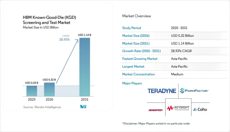
據 Mordor Intelligence 稱,HBM KGD(已知良好模具)篩檢測試市場預計將從 2025 年的 2.5 億美元成長到 2026 年的 3.2 億美元,到 2031 年達到 11.4 億美元,預計 2026 年至 2031 年的複合成長率93%。
本報告按測試階段(例如,晶圓級測試)、測試儀類型(例如,記憶體測試儀)、HBM 代數(例如,HBM2、HBM2E、HBM3)、測試技術(例如,基於嵌入式自診斷 (BIST)的篩檢)、應用(例如,設備)、最終用戶行業(例如,記憶體製造商)和地區進行細分。市場預測以美元 (USD) 為單位。
全球 HBM KGD(已知良品)篩檢測試市場趨勢及洞察
對人工智慧加速器需求的增加將推動KGD篩檢的加強。
HBM KGD(已知良品晶片)篩檢和測試市場正在擴張。這是因為在人工智慧加速器中,HBM 正逐漸成為核心效能的關鍵組件,而不僅僅是可選的記憶體升級。這種轉變使得晶片和堆疊故障的影響更加嚴重,因為一個缺陷就可能中斷整個運算模組的運行,而運算模組的成本遠高於單一記憶體組件。 FormFactor 預測,到 2026 年,人工智慧和 HBM 將改變半導體測試的重點,更加重視早期缺陷消除、良率穩定性和封裝級成本控制。客戶對設備的認證方式也面臨類似的壓力。更嚴格的篩檢不再是後端品質方面的偏好,而是高價值人工智慧硬體的商業性要求之一。隨著人工智慧伺服器部署的擴展,HBM KGD(已知良品晶片)篩檢和測試市場正受益於單件需求的成長以及每個設備篩檢步驟數量的增加。因此,即使晶圓產量的增加本身並不能完全解釋設備和產能擴張的速度,測試需求仍然很高。
一種用於保護多晶片良率的「左移」測試策略
HBM KGD(已知合格晶片)篩檢和測試市場也正受到製造流程中篩檢時間提前這一明顯趨勢的影響。 FormFactor 在 2026 年 5 月指出,早期測試策略至關重要,因為它決定了製造出的晶片是否能以「經過驗證認證的材料」的身份進入堆疊流程,從而保障下游製程的良率和成本。隨著堆疊設計從低層設計發展到 12 層和 16 層設計,這一邏輯變得更加重要,因為僅僅一個缺陷晶片就可能危及組裝產品價值的很大一部分。西門子 EDA 在 2026 年 4 月表示,HBM4 將把基礎晶片的生產方式轉變為邏輯代工廠式的方法,從而改變測試程序的架構。這使得在晶片、堆疊和封裝階段進行持續檢驗變得更加關鍵。實際上,這意味著 HBM“KGD(已知合格晶片)”篩檢測試市場不再僅僅關注生產線上某個環節的合格/不合格判定。隨著整合價值的提高,以一系列保護閘門為中心的系統對於防止缺陷累積變得越來越重要。
先進的ATE和探針基礎設施高成本
HBM KGD(已知良品晶片)篩檢和測試市場仍面臨諸多挑戰。這是因為對先進的記憶體測試、探測和處理系統進行認證成本高昂,且難以大規模部署。 Advantest 於 2025 年 12 月推出的 M5241 記憶體處理設備支援多達 512 個平行測試站點,吞吐量高達每小時 46,000 個單元,充分展現了現代基礎設施的專業化程度。 Aehr 在 2025 年 8 月下的評估訂單也表明,新專案可能需要客製化的接觸器設計和高於常規的電流供應,這要求在標準測試插件之外投入更多研發精力。 Technoprobe 在 2025 年資本市場日上的演講進一步強調了在先進探測環境中垂直整合 MEMS 能力的重要性,指出不僅設備所有權,強大的供應鏈也同樣重要。這種情況有利於能夠透過大規模生產分攤工程成本的大型記憶體製造商以及資質優良的合作夥伴。小規模的參與企業也可以進入 HBM KGD(已知良好模具)篩檢測試市場,但通常是透過更有限的角色或服務模式,而不是建立完整的內部平台。
細分市場分析
到2025年,晶圓級測試將佔據測試階段44.13%的最大佔有率,成為HBM KGD(已知良品晶片)篩檢測試市場中的第一個經濟控制點。這種主導地位反映了流程中一個簡單的成本邏輯:在堆疊之前檢測缺陷可以防止更昂貴的材料進入後續製程。 FormFactor指出,到2026年,初步篩檢將決定製造的晶片是否作為合格材料進入堆疊工藝,這表明晶圓級測試在下游工藝的良率穩定性方面發揮直接作用。在HBM KGD(已知良品晶片)篩檢測試市場中,晶圓級決策不僅影響良率,也影響未來每個堆疊投入的資金、處理時間和封裝組裝工作量。正因如此,儘管對晶圓級以外的檢驗需求不斷成長,晶圓級測試仍然是核心階段。
測試階段的其他構成比也在不斷擴展。這是因為,在先進的HBM專案中,後端檢驗環節不可或缺。隨著HBM4引入基於邏輯晶圓代工廠的晶片,並採用更複雜的整合製程(僅靠晶圓篩檢無法完全覆蓋),封裝級和系統級工作仍然至關重要。堆疊晶片測試是成長最快的領域,到2031年複合年成長率將達到29.67%,這反映了在最終封裝組裝之前進行「已知良好堆疊(KGS)」檢驗的價值日益成長。隨著堆疊高度的增加,以及客戶對裝置進入CoWoS和其他先進封裝製程之前可靠性的要求越來越高,這種需求也在不斷成長。 JEDEC的HBM4框架透過正式定義更嚴格的堆疊配置來支援這一方向,這自然而然地擴展了中期檢驗階段的作用。因此,在 HBM KGD(已知良好模具)篩檢測試市場中,每個階段的比例都在擴大,這是構成比這樣的明確認知:“早期篩檢可以節省成本,而後期篩檢可以保護通過堆疊和整合創造的更大價值。”
到2025年,記憶體測試儀將佔據38.23%的市場佔有率,成為測試儀類型中最大的細分市場。這主要得益於其在晶圓測試、功能篩檢以及跨越多代HBM晶片的認證週期中發揮的關鍵作用。這種主導地位源自於其豐富的部署經驗,以及傳統記憶體測試在HBM KGD(已知良品晶片)篩檢和測試市場中仍然是日常生產決策的核心。愛德萬測試2025年下半年的產品趨勢表明,供應商將繼續鞏固這一基礎,尤其是在需要高平行處理能力和穩定吞吐量的高效能AI記憶體元件領域。此外,由於每一代新的HBM晶片仍需要大量的電氣特性表徵和量產認證測試,記憶體測試儀的重要性依然不減。因此,即使新的測試方法日益普及,記憶體測試儀在HBM KGD(已知良品晶片)篩檢和測試市場中仍將保持穩固的地位。
老化測試系統是成長最快的測試設備類型,預計到 2031 年的複合年成長率將達到 29.58%,這反映出市場正轉向儘早消除昂貴的 AI 和 HBM 裝置中的潛在缺陷。 Aehr 的 2025 年評估訂單資料顯示,當下游故障成本變得不可接受時,客戶願意測試新的晶圓級老化測試方案。老化測試不再僅被視為最終的可靠性評估步驟;在 HBM KGD(已知良品晶片)篩檢測試市場中,它擴大扮演著「保護門」的角色,在先進封裝技術確定其進一步價值之前,它至關重要。探針卡和晶圓探針系統在這一趨勢中仍然不可或缺,因為精確的接觸、穩定的電流供應和可重複的機械性能對於更嚴格的篩檢仍然至關重要。 Technoprobe 的 2025 年擴張計劃表明,供應商也看到了在支援不斷成長的測試負載的接觸層方面持續存在的商機。因此,記憶體測試儀在目前的測試儀市場中仍然佔據主導地位,但隨著老化測試系統的作用越來越接近生產經濟的核心,這種差距正在縮小。
區域分析
到2025年,亞太地區將佔全球銷售額的83.49%,佔據HBM KGD(已知良品晶片)篩檢和測試市場的最大佔有率。同時,亞太地區也將成為成長最快的區域市場,到2031年複合年成長率將達到29.78%。該地區的主導地位得益於其HBM生產、測試設備供應和先進封裝產能的集中。韓國仍然是重要的樞紐,領先的HBM製造商推動了大部分初始認證工作,並滿足了對先進篩檢系統的大部分需求。台灣憑藉晶圓代工廠和封裝能力發揮著至關重要的整合作用,其測試基礎設施也是更廣泛的HBM發布流程的一部分。日本正透過其記憶體測試、探針和測量技術能力來加強其區域基礎,而中國則處於認證流程的早期階段,仍在建立其本土的HBM測試能力。
此外,亞太地區正透過政策支援和設施升級,鞏固其在HBM KGD(已知良品晶片)篩檢和測試市場的長期地位。截至2025年12月,日本半導體相關資本投資計畫在常規預算中總額為4.5兆日圓(約301億美元),補充預算中總額為6.3兆日圓(約421億美元)。這種支出環境有助於維持亞太地區整個供應鏈對測試設備、探針技術和製程能力的需求。因此,HBM KGD(已知良品晶片)篩檢和測試市場不僅在生產佔有率上集中於亞太地區,而且還擁有該地區最強大的製造、整合和供應商準備能力。這造就了其他地區短期內難以超越的結構性優勢。
儘管預計到2025年北美市場佔有率將有所下降,但其戰略地位依然重要,因為對超大規模資料中心業者的需求以及測試項目的主導將影響HBM KGD(已知良品晶片)篩檢和測試市場的發展。該地區匯集了眾多主要的設備和解決方案供應商,並透過人工智慧基礎設施客戶的購買力在認證要求的製定中發揮著重要作用。 Aehr在加州進行的晶圓級老化測試表明,即使北美在直接HBM晶圓生產方面落後於亞太地區,它仍然能夠影響早期篩檢方法。歐洲和南美洲的規模仍然較小,其中歐洲繼續透過Technoprobe等探針和測量專家發揮重要作用。同時,中東和非洲仍處於早期階段,它們的重要性更與下游人工智慧系統需求相關,而非上游HBM篩檢能力。
其他好處:
- Excel格式的市場預測(ME)表
- 3個月的分析師支持
目錄
第1章:引言
- 研究假設和市場定義
- 調查範圍
第2章:調查方法
第3章執行摘要
第4章 市場狀況
- 市場概覽
- 市場促進因素
- 對人工智慧加速器的需求不斷成長,活性化篩檢。
- 採用左移測試策略以確保多晶片良率
- HBM 堆疊的高度不斷增加,對缺陷控制的需求也日益成長。
- 擴大晶圓級老化測試的應用範圍,以消除潛在缺陷
- 由於對訊號完整性和電流的要求更加嚴格,測試範圍也隨之擴大。
- HBM4 認證流程的日益複雜導致了更高的堆疊前檢驗成本。
- 市場限制因素
- 先進的ATE和探針基礎設施高成本
- 高水準並行處理下的吞吐量限制
- 全速測試中的熱限制和電源限制
- 過度篩檢或假陽性導致產量損失的風險
- 產業價值鏈分析
- 監理情勢
- 技術展望
- 波特五力分析
- 宏觀經濟因素對市場的影響
第5章 市場規模與成長預測
- 測試階段
- 晶圓級測試
- 測試疊層模具
- 包級測試
- 系統級測試
- 按測試員類型
- 記憶體測試器
- 晶圓探針系統
- 探針卡
- 老化系統
- 按世代分類的 HBM
- HBM2,HBM2E
- HBM3
- HBM3E
- HBM4
- 測試技術
- 常規電氣測試
- 基於嵌入式自測(BIST)的篩檢
- 晶圓級老化
- 利用先進的探針和測量技術進行測試
- 透過使用
- 人工智慧和機器學習
- 高效能運算
- 遊戲和圖形處理
- 網路和通訊設備
- 汽車和運輸業
- 按最終用途行業分類
- 記憶體製造商
- 垂直整合設備製造商(IDM)
- 鑄造廠
- 半導體組裝和測試服務 (OSAT)
- 按地區
- 北美洲
- 美國
- 加拿大
- 墨西哥
- 歐洲
- 德國
- 英國
- 法國
- 義大利
- 其他歐洲國家
- 亞太地區
- 中國
- 日本
- 韓國
- 台灣
- 印度
- 其他亞太國家
- 南美洲
- 中東和非洲
- 北美洲
第6章 競爭情勢
- 市場集中度
- 策略趨勢
- 市佔率分析
- 公司簡介
- Teradyne Inc.
- Advantest Corporation
- FormFactor, Inc.
- Cohu, Inc.
- Keysight Technologies, Inc.
- TECHWING INC.
- DI Corporation
- Shenzhen SEICHI Technologies Co., Ltd.
- Wuhan Jingce Electronic Group Co., Ltd.
- Suzhou Secote Precision Electronic Co., Ltd.
- Chroma ATE Inc.
- SPEA SpA
- Tokyo Electron Limited
- Onto Innovation Inc.
- Kulicke and Soffa Industries, Inc.
- ASMPT Limited
第7章 市場機會與未來展望
According to Mordor Intelligence, the HBM known-Good-Die (KGD) screening and Test Market size is expected to increase from USD 0.25 billion in 2025 to USD 0.32 billion in 2026 and reach USD 1.14 billion by 2031, growing at a CAGR of 28.93% over 2026-2031.
This report is Segmented by Test Stage (Wafer-Level Testing, and More), Tester Type (Memory Tester, and More), HBM Generation (HBM2 and HBM2E, HBM3, and More), Test Technology (Built-In Self-Test Based Screening, and More), Application (Equipment, and More), End-Use Industry (Memory Manufacturers, and More), and Geography. The Market Forecasts are Provided in Terms of Value (USD).
Global HBM Known-Good-Die (KGD) Screening and Test Market Trends and Insights
Rising AI Accelerator Demand Increasing KGD Screening Intensity
The HBM known-good-die (KGD) screening and test market is moving higher because AI accelerators now rely on HBM as a core performance building block rather than an optional memory upgrade. That shift raises the penalty for any die or stack failure, because defects can disrupt a much more expensive compute module rather than a stand-alone memory component. FormFactor stated in 2026 that AI and HBM are changing semiconductor test priorities by pushing more attention toward early defect removal, yield stability, and package-level cost protection. The same pressure is evident in how customers qualify devices, as stronger screening has become part of the commercial requirements for high-value AI hardware rather than a back-end quality preference. As AI server deployments widen, the HBM known-good-die (KGD) screening and test market is benefiting from both higher unit demand and more screening steps per device. This keeps test demand elevated even when wafer output growth alone does not fully explain the pace of equipment and capacity additions.
Shift-Left Test Strategies to Protect Multi-Die Yield
The HBM known-good-die (KGD) screening and test market is also being shaped by a clear move toward earlier screening points in the production flow. FormFactor noted in May 2026 that early test strategies are critical because they determine whether manufactured dies enter stacking as proven-qualified material, which protects downstream yield and costs. That logic becomes stronger as stacks move from fewer layers to 12- and 16-high designs, because a single weak die can compromise a much larger portion of the assembled value. Siemens EDA showed in April 2026 that HBM4 changes the test program architecture by shifting the base die toward a logic-foundry approach, making validation continuity across die, stack, and package stages more important. In practice, this means the HBM known-good-die (KGD) screening and test market is no longer centered solely on pass-or-fail screening at a single point in the line. It is increasingly organized around a sequence of protection gates that try to keep scrap from compounding as integration value rises.
High Cost of Advanced ATE and Probe Infrastructure
The HBM known-good-die (KGD) screening and test market still faces a meaningful barrier because advanced memory test, probing, and handling systems are expensive to qualify and difficult to deploy at scale. Advantest's December 2025 launch of the M5241 Memory Handler, with support for up to 512 parallel test sites and throughput up to 46,000 units per hour, shows how specialized the latest infrastructure has become. Aehr's August 2025 evaluation order also showed that new programs can require custom contactor design and unusually high current delivery, which adds another layer of development effort beyond standard test insertion. Technoprobe's 2025 Capital Market Day presentation further underscored the need for vertically integrated MEMS capabilities in advanced probe environments, suggesting that supply depth matters as much as simple equipment ownership. These conditions favor large memory manufacturers and well-qualified partners that can spread engineering costs across high volumes. Smaller participants can still enter the HBM known-good-die (KGD) screening and test market, but they often do so through narrower roles or service models rather than full in-house platform builds.
Other drivers and restraints analyzed in the detailed report include:
- Higher HBM Stack Heights Raising Defect Containment Needs
- Growing Use of Wafer-Level Burn-In for Latent Defect Removal
- Limited Throughput at High Parallelism Levels
For complete list of drivers and restraints, kindly check the Table Of Contents.
Segment Analysis
Wafer-level testing held the largest share among test-stage segments at 44.13% in 2025, making it the first economic control point in the HBM known-good-die (KGD) screening and test market. That lead reflects the simple cost logic of the flow, since defects caught before stacking prevent more expensive material from moving into later process steps. FormFactor stated in 2026 that early screening determines whether manufactured dies reach stacking as qualified material, which gives wafer-level testing a direct role in downstream yield stability. In the HBM known-good-die (KGD) screening and test market, wafer-level decisions shape not only yield but also the capital, handling time, and package assembly effort committed to each future stack. This is why the segment remained the anchor stage even as validation demands broadened beyond the wafer.
The rest of the test-stage mix is still expanding because later validation points cannot be removed from advanced HBM programs. Package-level and system-level work remain relevant as HBM4 introduces a logic-foundry base die and a more complex integration path that wafer screening alone cannot fully cover. Stacked-die testing is the fastest-growing segment, with a 29.67% CAGR through 2031, underscoring the growing value of known-good-stack verification before final package assembly. The need grows as stack height increases and as customers seek more confidence before devices enter CoWoS and other advanced packaging flows. JEDEC's HBM4 framework supports this direction by formalizing more demanding stack configurations, which naturally widens the role of intermediate validation gates. For the HBM known-good-die (KGD) screening and test market, the stage mix is therefore widening around a clear idea, early screens save money, but later screens protect the much larger value created by stacking and integration.
Memory testers were the largest tester type segment in 2025, with a 38.23% share, supported by their roles across wafer test, functional screening, and qualification cycles spanning multiple HBM generations. Their lead comes from broad installed use and the fact that conventional memory testing remains central to day-to-day production decisions in the HBM known-good-die (KGD) screening and testing market. Advantest's product activity in late 2025 showed how vendors continue to strengthen this base, especially for high-performance AI memory devices that need higher parallelism and steadier throughput. Memory testers also remain relevant because each new HBM generation still requires a substantial body of electrical characterization and production-qualified test content. That keeps the segment firmly embedded in the HBM known-good-die (KGD) screening and test market even as newer methods gain ground.
Burn-in systems are the fastest-growing tester type, with a 29.58% CAGR through 2031, reflecting the shift toward earlier removal of latent defects in expensive AI and HBM devices. Aehr's 2025 evaluation order showed that customers are willing to test new wafer-level burn-in paths when the cost of downstream failure becomes too high to ignore. Burn-in is no longer treated only as a late reliability step, because in the HBM known-good-die (KGD) screening and test market it increasingly acts as a protection gate before advanced packaging locks in more value. Probe cards and wafer probe systems remain essential around this trend, since stronger screening still depends on accurate contact, stable current delivery, and repeatable mechanical performance. Technoprobe's 2025 expansion plans underline that suppliers also see a durable opportunity in the contact layer that supports these rising test loads. The result is a tester landscape where memory testers still lead today, but burn-in systems are closing the gap because their role is moving closer to the center of production economics.
Complete Report Scope:
- By Test Stage
- Wafer-Level Testing
- Stacked-Die Testing
- Package-Level Testing
- System-Level Testing
- By Tester Type
- Memory Tester
- Wafer Probe Systems
- Probe Cards
- Burn-In Systems
- By HBM Generation
- HBM2 and HBM2E
- HBM3
- HBM3E
- HBM4
- By Test Technology
- Conventional Electrical Testing
- Built-In Self-Test Based Screening
- Wafer-Level Burn-In
- Advanced Probe and Metrology-Assisted Test
- By Application
- Artificial Intelligence and Machine Learning
- High-Performance Computing
- Gaming and Graphics Processing
- Network and Communication Equipment
- Automotive and Transportation
- By End-Use Industry
- Memory Manufacturers
- Integrated Device Manufacturers (IDMs)
- Foundries
- Outsourced Semiconductor Assembly and Test (OSAT)
- By Geography
- North America
- United States
- Canada
- Mexico
- Europe
- Germany
- United Kingdom
- France
- Italy
- Rest of Europe
- Asia-Pacific
- China
- Japan
- South Korea
- Taiwan
- India
- Rest of Asia-Pacific
- South America
- Middle East and Africa
- North America
Geography Analysis
Asia-Pacific commanded 83.49% of revenue in 2025, giving it the largest share of the HBM known-good-die (KGD) screening and testing market, and it is also the fastest-growing regional segment at a 29.78% CAGR through 2031. The region leads because HBM production, test equipment supply, and advanced packaging capacity are all concentrated there. South Korea remains the main anchor, since the leading HBM manufacturers drive most of the early qualification work and much of the demand for advanced screening systems. Taiwan plays a critical integration role through its foundry and packaging capacity, making its test infrastructure part of the wider HBM release path. Japan is strengthening its regional base through memory test, probe, and metrology capabilities, while China is still building local HBM test capacity from an earlier position on the qualification curve.
Asia-Pacific also benefits from policy support and equipment depth that reinforce its long-term position in the HBM known-good-die (KGD) screening and test market. Japan's semiconductor-related capital investment program totaled JPY 4.5 trillion (USD 30.1 billion) under the regular budget and JPY 6.3 trillion (USD 42.1 billion) under supplementary allocations as of December 2025. That spending environment helps sustain demand for test equipment, probe technology, and process capability across the regional supply chain. The HBM known-good-die (KGD) screening and test market is therefore not only concentrated in Asia-Pacific by production share, but also supported there by the deepest combination of manufacturing, integration, and supplier readiness. This creates a structural advantage that other regions are unlikely to close quickly.
North America held a smaller share in 2025, but it remains strategically important because hyperscaler demand and test program ownership influence how the HBM known-good-die (KGD) screening and test market evolves. The region is home to major equipment and solution providers, and it also shapes qualification requirements through the buying power of AI infrastructure customers. Aehr's wafer-level burn-in activity in California shows that North America can influence early-stage screening methods even without matching Asia-Pacific in direct HBM wafer output. Europe and South America remain smaller, though Europe keeps a meaningful role through probe and metrology specialists such as Technoprobe, while the Middle East and Africa are still early-stage participants whose relevance is linked more to downstream AI system demand than to upstream HBM screening capacity.
- Teradyne Inc.
- Advantest Corporation
- FormFactor, Inc.
- Cohu, Inc.
- Keysight Technologies, Inc.
- TECHWING INC.
- DI Corporation
- Shenzhen SEICHI Technologies Co., Ltd.
- Wuhan Jingce Electronic Group Co., Ltd.
- Suzhou Secote Precision Electronic Co., Ltd.
- Chroma ATE Inc.
- SPEA S.p.A.
- Tokyo Electron Limited
- Onto Innovation Inc.
- Kulicke and Soffa Industries, Inc.
- ASMPT Limited
Additional Benefits:
- The market estimate (ME) sheet in Excel format
- 3 months of analyst support
TABLE OF CONTENTS
1 INTRODUCTION
- 1.1 Study Assumptions and Market Definition
- 1.2 Scope of the Study
2 RESEARCH METHODOLOGY
3 EXECUTIVE SUMMARY
4 MARKET LANDSCAPE
- 4.1 Market Overview
- 4.2 Market Drivers
- 4.2.1 Rising AI Accelerator Demand Increasing KGD Screening Intensity
- 4.2.2 Shift-Left Test Strategies to Protect Multi-Die Yield
- 4.2.3 Higher HBM Stack Heights Raising Defect Containment Needs
- 4.2.4 Growing Use of Wafer-Level Burn-In For Latent Defect Removal
- 4.2.5 Tight Signal Integrity and Current Requirements Expanding Test Content
- 4.2.6 HBM4 Qualification Complexity Increasing Pre-Stack Validation Spend
- 4.3 Market Restraints
- 4.3.1 High Cost of Advanced ATE and Probe Infrastructure
- 4.3.2 Limited Throughput at High Parallelism Levels
- 4.3.3 Thermal and Power Delivery Constraints During Full-Rate Testing
- 4.3.4 Yield Loss Risk From Over-Screening and False Rejects
- 4.4 Industry Value Chain Analysis
- 4.5 Regulatory Landscape
- 4.6 Technological Outlook
- 4.7 Porter's Five Forces Analysis
- 4.7.1 Threat of New Entrants
- 4.7.2 Bargaining Power of Suppliers
- 4.7.3 Bargaining Power of Buyers
- 4.7.4 Threat of Substitutes
- 4.7.5 Intensity of Competitive Rivalry
- 4.8 Impact of Macroeconomic Factors on the Market
5 MARKET SIZE AND GROWTH FORECASTS (VALUE)
- 5.1 By Test Stage
- 5.1.1 Wafer-Level Testing
- 5.1.2 Stacked-Die Testing
- 5.1.3 Package-Level Testing
- 5.1.4 System-Level Testing
- 5.2 By Tester Type
- 5.2.1 Memory Tester
- 5.2.2 Wafer Probe Systems
- 5.2.3 Probe Cards
- 5.2.4 Burn-In Systems
- 5.3 By HBM Generation
- 5.3.1 HBM2 and HBM2E
- 5.3.2 HBM3
- 5.3.3 HBM3E
- 5.3.4 HBM4
- 5.4 By Test Technology
- 5.4.1 Conventional Electrical Testing
- 5.4.2 Built-In Self-Test Based Screening
- 5.4.3 Wafer-Level Burn-In
- 5.4.4 Advanced Probe and Metrology-Assisted Test
- 5.5 By Application
- 5.5.1 Artificial Intelligence and Machine Learning
- 5.5.2 High-Performance Computing
- 5.5.3 Gaming and Graphics Processing
- 5.5.4 Network and Communication Equipment
- 5.5.5 Automotive and Transportation
- 5.6 By End-Use Industry
- 5.6.1 Memory Manufacturers
- 5.6.2 Integrated Device Manufacturers (IDMs)
- 5.6.3 Foundries
- 5.6.4 Outsourced Semiconductor Assembly and Test (OSAT)
- 5.7 By Geography
- 5.7.1 North America
- 5.7.1.1 United States
- 5.7.1.2 Canada
- 5.7.1.3 Mexico
- 5.7.2 Europe
- 5.7.2.1 Germany
- 5.7.2.2 United Kingdom
- 5.7.2.3 France
- 5.7.2.4 Italy
- 5.7.2.5 Rest of Europe
- 5.7.3 Asia-Pacific
- 5.7.3.1 China
- 5.7.3.2 Japan
- 5.7.3.3 South Korea
- 5.7.3.4 Taiwan
- 5.7.3.5 India
- 5.7.3.6 Rest of Asia-Pacific
- 5.7.4 South America
- 5.7.5 Middle East and Africa
- 5.7.1 North America
6 COMPETITIVE LANDSCAPE
- 6.1 Market Concentration
- 6.2 Strategic Moves
- 6.3 Market Share Analysis
- 6.4 Company Profiles (includes Global Level Overview, Market Level Overview, Core Segments, Financials as available, Strategic Information, Market Rank/Share, Products and Services, Recent Developments)
- 6.4.1 Teradyne Inc.
- 6.4.2 Advantest Corporation
- 6.4.3 FormFactor, Inc.
- 6.4.4 Cohu, Inc.
- 6.4.5 Keysight Technologies, Inc.
- 6.4.6 TECHWING INC.
- 6.4.7 DI Corporation
- 6.4.8 Shenzhen SEICHI Technologies Co., Ltd.
- 6.4.9 Wuhan Jingce Electronic Group Co., Ltd.
- 6.4.10 Suzhou Secote Precision Electronic Co., Ltd.
- 6.4.11 Chroma ATE Inc.
- 6.4.12 SPEA S.p.A.
- 6.4.13 Tokyo Electron Limited
- 6.4.14 Onto Innovation Inc.
- 6.4.15 Kulicke and Soffa Industries, Inc.
- 6.4.16 ASMPT Limited
7 MARKET OPPORTUNITIES AND FUTURE OUTLOOK
- 7.1 White-Space and Unmet-Need Assessment


