

 |
市場調查報告書
商品編碼
2099447
HBM製造設備:市場佔有率分析、產業趨勢與統計、成長預測(2026-2031年)HBM Manufacturing Equipment - Market Share Analysis, Industry Trends & Statistics, Growth Forecasts (2026 - 2031) |
||||||

※ 本網頁內容可能與最新版本有所差異。詳細情況請與我們聯繫。
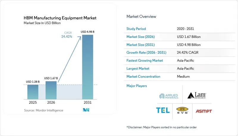
據 Mordor Intelligence 稱,HBM 製造設備市場預計將從 2025 年的 12.8 億美元成長到 2026 年的 16.7 億美元,到 2031 年達到 49.8 億美元,預計 2026 年至 2031 年的複合年成長率為 24.40%。
本報告按設備類型(TSV蝕刻設備等)、鍵合技術(熱壓鍵合、混合鍵合等)、HBM代數(HBM2E、HBM3、HBM3E等)、堆疊方式(晶片到晶圓、晶圓到晶圓、晶片到晶片)、最終用戶(記憶體製造商、代工廠、OSAT廠商)和地區進行細分。市場預測以美元計價。
全球高密度玻爾茲曼造粒機製造設備市場趨勢及洞察
AI記憶體的堆疊密度正在推動對TSV和混合鍵合設備的需求。
如今,HBM製造設備市場與AI加速器的普及應用之間的關聯性已遠超傳統DRAM的更新換代週期。隨著AI模型日趨複雜,記憶體堆疊正朝著更高密度的TSV陣列、更窄的鍵合間距以及更先進的平坦化製程發展,這導致每片晶圓的設備使用量不斷增加。應用材料公司推出了Nokota Vmax 2電化學電鍍系統,該系統具備自適應圖案調整功能,旨在解決超細間距節點上TSV陣列的電鍍差異問題。這點至關重要,因為在先前的微型化階段可以接受的缺陷,如今卻會降低多晶片堆疊的整體良率。因此,HBM製造設備市場的需求與運算藍圖的發展方向一致,NVIDIA的Rubin平台規格(8層HBM4堆疊,總合頻寬Terabyte/s)已開始影響供應商的計畫。這些因素共同作用,使得設備需求在整個預測期內保持穩定。
向 HBM4 和低間距互連過渡
HBM4 透過過渡到 2048 位元介面並將每個堆疊的頻寬提升至每秒 2 Terabyte以上,進一步提高了 HBM 製造設備市場的技術門檻。應對這些變化需要能夠處理厚度約為 30微米的單一 DRAM 晶片,同時保持整個堆疊的對準精度在 100 奈米以內的設備。 Besi 在 2026 年第一季簡報中指出,三大記憶體製造商均在基於相同的客戶需求評估混合鍵合設備,目標是在 2027 年實現混合鍵結堆疊的商業部署。隨著 HBM4 基礎晶片不再完全局限於傳統的記憶體製造流程,而是開始在台積電的先進邏輯節點上生產,台灣的需求也不斷成長。這導致了設備配置的變化,因為鍵合、CMP、測量和 TSV 製程必須同時滿足記憶體和代工廠的認證標準。因此,HBM 製造設備市場正在經歷重組,不僅是因為堆疊數量的增加,還因為支援高度邏輯整合的基礎晶片需要更廣泛的製程整合。
極高的資本投入強度和較長的認證週期
HBM製造設備市場的主要限制因素是下一代鍵結系統的高成本以及這些系統為確保生產良率所需的漫長認證週期。這種成本結構導致採購延遲,即使裝置需求強勁,因為設備選擇必須與客戶晶圓廠內漫長的檢驗週期相符。此外,這種負擔並不均衡,因為擁有成熟製程合作關係的大型記憶體製造商可以比封裝領域的新進入者或OSAT(外包組裝公司)更快地推進。在某些情況下,新參與企業可能需要超過18個月的認證才能使其生產線投入運作。因此,由於資本投資受限和認證風險,客戶群較為狹窄,HBM製造設備市場的成長速度低於僅基於終端需求的預期。
細分市場分析
到2025年,晶圓/晶片鍵合設備將佔據HBM製造設備市場33.81%的佔有率,成為現有生產線中最大的設備類別。這一主導地位主要歸功於SK海力士、三星和美光等公司對HBM3E的大規模生產,在這些公司中,熱壓鍵合機仍然是晶片堆疊的核心設備。此外,較長的認證週期也鞏固了這一地位,因為一旦鍵合設備被引入大規模生產線,就很難更換。 TSV蝕刻和CMP設備是重要的相關製程領域,其中蝕刻形成通孔結構,而CMP則對錶面進行處理,為後續的鍵結製程做準備。在HBM製造設備市場,能夠同時支援這些緊密相關製程的產能和重複性的供應商將持續保持優勢。
預計2026年至2031年間,臨時鍵結和解鍵合設備將以25.38%的複合年成長率快速成長,這反映了DRAM晶片厚度不斷減少和堆疊層數不斷增加的趨勢。 EV集團表示,其紅外線釋放技術能夠以奈米級精度對矽進行雷射解鍵合,因此無需在先進的臨時鍵合製程中使用玻璃基板。隨著堆疊層數的增加和晶圓厚度的減小,處理小於30微米的晶片變得越來越具有挑戰性,因此這項技術意義重大。 SUSS MicroTec在臨時鍵結和解鍵結領域保持強大的市場地位,在當前HBM大規模生產擴張和未來的晶圓級堆疊項目中都發揮關鍵作用。隨著客戶尋求縮短複雜封裝製程的整合時間,這些設備之間的互通性變得越來越重要。因此,HBM製造設備產業越來越重視那些能夠將新製程無縫整合到現有生產線的供應商。因此,HBM製造設備市場的擴張不僅是由於機器數量的增加,也是由於對相容的多層級平台的需求不斷成長。
到2025年,熱壓鍵合將佔HBM製造設備市場72.46%的佔有率,這反映出其在HBM3E生產中幾乎被普遍採用。由於其能夠利用已知的熱壓控制曲線處理間距為9至55微米的堆疊式DRAM組件,因此仍是生產標準。這表明,在HBM製造設備市場,對單一客戶的依賴仍然會對主要鍵合供應商的經濟效益產生顯著影響。由於在研磨、TSV暴露和金屬化製程中需要更安全的操作,瞬態晶圓鍵合技術和解鍵合技術也與熱壓鍵結生產線同步成長。
混合鍵結技術預計在2026年至2031年間將以25.89%的複合年成長率成長,並有望成為成長最快的鍵結技術,因為堆疊高度將超過目前熱壓縮技術的極限。 SUSS MicroTec公司發布了XBC300 Gen2 D2W平台,該平台是一個整合系統,涵蓋晶圓間鍵合、批次晶片-晶圓鍵合和順序晶片-晶圓鍵合。該平台實現了±100奈米的對準精度。三星正在透過SEMES自主研發混合鍵合技術,而Besi公司已向三大記憶體製造商交付了評估樣機。這一轉變意義重大,因為零間隙銅-銅鍵合可以比基於凸塊的互連實現更高的單位面積頻寬密度。然而,混合鍵合的成本是覆晶鍵合的2到3倍,需要透過提高良率來降低成本,因此其應用仍將分階段進行。因此,HBM製造設備產業正進入一個傳統鍵合線和下一代鍵合線並存的時期。這種共存使得 HBM 製造設備市場對那些既能滿足當前大規模生產需求又能確保未來認證的供應商具有吸引力。
區域分析
預計到2025年,亞太地區將佔據全球HBM製造設備市場規模的82.14%,並將以25.28%的複合年成長率成長至2031年。韓國在該地區保持核心地位,擁有最大的HBM生產基地,並在封裝和製造領域進行了大量新的投資。隨著HBM晶片生產轉向高度邏輯整合的生產線,台灣的重要性日益凸顯,這得益於台積電先進的代工服務。日本也扮演雙重角色,一方面透過SCREEN、DISCO、ULVAC和東京電子等國內設備供應商,另一方面透過美光在廣島不斷擴張的HBM業務。由於亞太地區擁有龐大的記憶體生產能力、高度集中的供應商以及完善的認證體系,HBM製造設備市場仍高度集中於該地區。中國正在持續建構其國內生態系統,但對先進封裝設備的出口限制仍限制其獲取世界級設備的管道。因此,與其直接挑戰主要區域需求中心的現有供應商,不如另闢蹊徑:本地設備開發。
儘管北美目前在HBM製造設備市場中的佔有率遠小於亞太地區,但隨著美國半導體產業的獎勵推動新產能的擴張,其長期地位正在不斷增強。美光計畫在紐約州奧農達加縣建造大規模製造地,並在博伊西持續擴張,美國正轉型成為未來鍵結、TSV和先進封裝設備的重要需求中心。歐洲雖然在記憶體生產方面的貢獻較小,但憑藉其供應商的實力,尤其是奧地利的EV集團和德國的SUSS MicroTec,仍扮演著重要角色。 EV集團在晶圓鍵合技術和層間轉移領域保持核心地位,而SUSS MicroTec正在開發混合鍵合技術,以滿足下一階段HBM製造設備市場的需求。荷蘭的Besi公司也佔有重要的戰略地位,三大記憶體製造商都對其混合鍵合設備給予了高度評價。
南美洲和中東及非洲目前僅佔HBM製造設備市場需求的一小部分。這兩個地區在HBM製造或先進封裝應用方面均缺乏顯著經驗,因此設備投資僅限於小規模測試和電子組裝需求。儘管沿岸地區部分地區的政府半導體專案和巴西的電子產品激勵計劃可能會促進長期封裝活動,但在目前的預測期內,預計不會出現大規模的HBM專用設備採購。然而,HBM製造設備市場地域集中度較高,主要競爭對手和投資活動仍集中在亞太地區,北美和歐洲的投資僅限於特定項目。
其他好處:
- Excel格式的市場預測(ME)表
- 3個月的分析師支持
目錄
第1章:引言
- 研究假設和市場定義
- 調查範圍
第2章:調查方法
第3章執行摘要
第4章 市場狀況
- 市場概覽
- 市場促進因素
- AI記憶體堆疊密度的不斷提高,推動了對TSV和混合鍵合設備的需求。
- 過渡到 HBM4 和更小間距互連
- 記憶體製造商提高先進封裝的產能。
- 對超光滑表面和無缺陷介面的需求日益成長
- 先進半導體製造設備供應鏈本地化
- TSV蝕刻、鍵結和CMP平台之間的製程整合。
- 市場限制因素
- 極高的資本投入率和較長的認證週期
- 高長寬比TSV和混合鍵合製程的良率敏感度
- 部署在主要儲存設施以外的單元數量有限。
- 記憶體製造商和OSAT之間工具介面的碎片化
- 產業供應鏈分析
- 監理情勢
- 技術展望
- 波特五力分析
- 宏觀經濟因素對市場的影響
第5章 市場規模與成長預測
- 依設備類型
- TSV蝕刻設備
- 晶圓/晶片鍵合設備
- CMP設備
- 臨時黏合和剝離裝置
- 測量和檢測設備
- 透過鍵合技術
- 熱壓黏接
- 混合鍵合
- 晶圓臨時鍵結和解鍵合
- 按世代分類的 HBM
- HBM2
- HBM2E
- HBM3
- HBM3E
- HBM4
- 層壓法
- 從晶片到晶圓
- 晶圓之間
- 死而復生
- 最終用戶
- 記憶體製造商
- 鑄造廠
- OSAT
- 按地區
- 北美洲
- 美國
- 其他北美國家
- 歐洲
- 德國
- 荷蘭
- 其他歐洲國家
- 亞太地區
- 中國
- 日本
- 韓國
- 台灣
- 其他亞太國家
- 南美洲
- 中東和非洲
- 北美洲
第6章 競爭情勢
- 市場集中度
- 策略趨勢
- Market Positing Analysis
- 公司簡介
- Applied Materials, Inc.
- Lam Research Corporation
- Tokyo Electron Limited
- EV Group Holding GmbH
- ASMPT Limited
- BE Semiconductor Industries NV
- Hanmi Semiconductor Co., Ltd.
- SCREEN Holdings Co., Ltd.
- KLA Corporation
- Onto Innovation Inc.
- SUSS MicroTec SE
- Shibaura Mechatronics Corporation
- DISCO Corporation
- Kulicke and Soffa Industries, Inc.
- Canon Inc.
- ULVAC, Inc.
- Ebara Corporation
- Hitachi High-Tech Corporation
- Plasma-Therm LLC
- Oxford Instruments plc
- Advanced Micro-Fabrication Equipment Inc. China
第7章 市場機會與未來展望
According to Mordor Intelligence, the HBM manufacturing equipment market size is expected to increase from USD 1.28 billion in 2025 to USD 1.67 billion in 2026 and reach USD 4.98 billion by 2031, growing at a CAGR of 24.40% over 2026-2031.
This report is Segmented by Equipment Type (TSV Etch Equipment, and More), Bonding Technology (Thermocompression Bonding, Hybrid Bonding, and More), HBM Generation (HBM2E, HBM3, HBM3E, and More), Stacking Method (Die-To-Wafer, Wafer-To-Wafer, and Die-To-Die), End User (Memory Makers, Foundries, and OSATs), and Geography. The Market Forecasts are Provided in Terms of Value (USD).
Global HBM Manufacturing Equipment Market Trends and Insights
AI Memory Stack Density Driving TSV And Hybrid Bonding Tool Demand
The HBM manufacturing equipment market is now tied more closely to AI accelerator deployment than to the older DRAM replacement cycle. Higher AI model complexity is pushing memory stacks toward denser TSV arrays, tighter bonding pitch, and more demanding planarization steps, which raises equipment intensity per wafer start. Applied Materials introduced the Nokota Vmax 2 electrochemical deposition tool with adaptive pattern tuning to address plating variation across TSV arrays at very fine pitch nodes. This matters because defects that were manageable at earlier geometries can now reduce yield across an entire multi-die stack. The HBM manufacturing equipment market is therefore seeing demand that follows compute roadmaps, as NVIDIA's Rubin platform specification for 8 HBM4 stacks and 22 terabytes per second of aggregate bandwidth is already influencing supplier planning. That combination makes tool demand both visible and durable through the forecast period.
Migration To HBM4 And Lower-Pitch Interconnects
HBM4 is raising the technical bar for the HBM manufacturing equipment market by moving to a 2,048-bit interface and pushing per-stack bandwidth above 2 terabytes per second. Those changes require tools that can handle individual DRAM dies measuring nearly 30 micrometers thick while maintaining alignment within sub-100-nanometer tolerances across the full stack. Besi stated in its Q1 2026 discussion that all 3 major memory manufacturers are evaluating hybrid bonding tools to the same customer requirement, with commercial deployment of hybrid-bonded stacks targeted for 2027. The transition is also expanding demand in Taiwan, as HBM4 base dies are being fabricated on advanced logic nodes at TSMC rather than remaining entirely within traditional memory flows. That changes the tool mix, since bonding, CMP, metrology, and TSV steps now need to satisfy both memory and foundry qualification standards. The HBM manufacturing equipment market is therefore being reshaped not only by higher stack counts, but also by the broader process integration required to support logic-rich base dies.
Extreme Capex Intensity And Long Qualification Cycles
A major limit on the HBM manufacturing equipment market is the high cost of next-generation bonding systems and the long qualification cycle needed before those tools can support production yield. That cost structure slows procurement even when device demand is strong, because tool decisions must be matched with long validation periods inside customer fabs. The burden is also uneven, since large memory makers with established process relationships can move faster than new packaging entrants or OSATs. In some cases, new participants may face qualification timelines of more than 18 months before a line becomes production-ready. The HBM manufacturing equipment market, therefore, grows more slowly than end demand alone would suggest, because capex discipline and qualification risk narrow the customer set.
Other drivers and restraints analyzed in the detailed report include:
- Advanced Packaging Capacity Additions By Memory Makers
- Rising Need For Ultra-Flat Surfaces And Defect-Free Interfaces
- Yield Sensitivity In High-Aspect-Ratio Tsv And Hybrid Bonding Flows
For complete list of drivers and restraints, kindly check the Table Of Contents.
Segment Analysis
Wafer/Die Bonding Equipment held 33.81% of the HBM manufacturing equipment market share in 2025, which made it the largest equipment category in current production lines. Its lead came from HBM3E volume manufacturing across SK hynix, Samsung, and Micron, where thermocompression bonders remain the central tool for die stacking. This position is also supported by long qualification cycles, because a fully approved bonding tool is difficult to displace once it is embedded in a high-volume line. TSV Etch Equipment and CMP Equipment followed as important linked process categories, since etch forms the via structure and CMP prepares the surface for later bonding stages. The HBM manufacturing equipment market continues to reward vendors that can support both throughput and repeatability in these tightly linked steps.
Temporary Bonding and Debonding Equipment is projected to grow the fastest, at a 25.38% CAGR from 2026 to 2031, reflecting the move toward thinner DRAM dies and taller stack designs. EV Group said its IR Layer Release technology enables nanometer-level precision laser debonding of silicon and eliminates the need for glass substrates in advanced temporary bonding flows. That matters because handling dies below 30 micrometers becomes more difficult as stack counts rise and wafer thinning intensifies. SUSS MicroTec has maintained a strong position in temporary bonding and debonding, which makes it relevant to both today's HBM ramps and future wafer-level stacking programs. Interoperability across these tool sets is becoming more important as customers try to reduce integration time across complex packaging flows. That is why the HBM manufacturing equipment industry is placing greater value on suppliers that can fit into an existing line without creating new process friction. The HBM manufacturing equipment market is therefore expanding not only through higher tool counts, but also through the growing need for compatible multi-step platforms.
Thermocompression bonding accounted for 72.46% of the HBM manufacturing equipment market in 2025, reflecting its near-universal use across HBM3E production. It remains the production standard because it can support stacked DRAM assembly at pitches of 9 to 55 micrometers with known heat and pressure control profiles. This shows how single-customer exposure can still define the economics of a major bonding supplier in the HBM manufacturing equipment market. Temporary wafer bonding and debonding also grow alongside thermocompression lines because it enables safer handling during grinding, TSV exposure, and metallization.
Hybrid bonding is projected to grow at a 25.89% CAGR from 2026 to 2031, making it the fastest-growing bonding technology as stack heights exceed current thermocompression limits. SUSS MicroTec introduced the XBC300 Gen2 D2W platform as an integrated system covering wafer-to-wafer, collective die-to-wafer, and sequential die-to-wafer bonding with alignment accuracy of plus or minus 100 nanometers. Samsung is developing hybrid bonding internally through SEMES, while Besi has already shipped evaluation units to all 3 major memory manufacturers. The shift is important because zero-gap copper-to-copper bonding allows higher bandwidth density per unit area than bump-based interconnects. Adoption will still move in phases, since hybrid bonding costs remain 2 to 3 times those of flip-chip bonding per die and must come down through yield improvement. The HBM manufacturing equipment industry is therefore entering a period where both legacy and next-generation bonding lines will coexist. That coexistence keeps the HBM manufacturing equipment market attractive for vendors that can serve current mass production while also securing future qualification wins.
Complete Report Scope:
- By Equipment Type
- TSV Etch Equipment
- Wafer/Die Bonding Equipment
- CMP Equipment
- Temporary Bonding and Debonding Equipment
- Metrology and Inspection Equipment
- By Bonding Technology
- Thermocompression Bonding
- Hybrid Bonding
- Temporary Wafer Bonding and Debonding
- By HBM Generation
- HBM2
- HBM2E
- HBM3
- HBM3E
- HBM4
- By Stacking Method
- Die-to-Wafer
- Wafer-to-Wafer
- Die-to-Die
- By End User
- Memory Makers
- Foundries
- OSATs
- By Geography
- North America
- United States
- Rest of North America
- Europe
- Germany
- Netherlands
- Rest of Europe
- Asia-Pacific
- China
- Japan
- South Korea
- Taiwan
- Rest of Asia-Pacific
- South America
- Middle East and Africa
- North America
Geography Analysis
Asia-Pacific accounted for 82.14% of the HBM manufacturing equipment market size in 2025 and is projected to grow at a 25.28% CAGR through 2031. South Korea remains the center of this regional position because it combines the largest HBM production base with major new commitments in packaging and fabrication. Taiwan is becoming increasingly important because TSMC's advanced foundry services are driving HBM base-die production onto logic-intensive manufacturing lines. Japan also plays a dual role through domestic equipment suppliers such as SCREEN, DISCO, ULVAC, and Tokyo Electron, as well as through Micron's HBM expansion in Hiroshima. The HBM manufacturing equipment market stays concentrated in Asia-Pacific because the region combines memory production, supplier density, and established qualification infrastructure. China is still building a more separate domestic ecosystem, but export controls on advanced packaging tools continue to limit its access to global best-in-class equipment. That is creating a parallel path for local tool development rather than a direct challenge to incumbent suppliers across the main regional demand centers.
North America still holds a much smaller share than Asia-Pacific in the current HBM manufacturing equipment market, but its long-term role is strengthening as U.S. semiconductor incentives support new capacity. Micron's plan to build major manufacturing capacity in Onondaga County, New York, along with expansion in Boise, shifts the United States toward a more meaningful future demand center for bonding, TSV, and advanced packaging tools. Europe contributes less through memory production and more through supplier strength, especially through EV Group in Austria and SUSS MicroTec in Germany. EV Group remains central in wafer bonding and layer transfer, while SUSS MicroTec is advancing hybrid bonding capabilities that align with the next stage of the HBM manufacturing equipment market. Besi in the Netherlands also holds a strategically important place because all 3 major memory producers are evaluating its hybrid bonding tools.
South America, the Middle East, and Africa account for only a minimal share of current demand in the HBM manufacturing equipment market. Neither region has a major installed base of HBM fabrication or advanced packaging capacity, so equipment spending remains limited to smaller testing and electronics assembly needs. Government semiconductor programs in parts of the Gulf and electronics incentive frameworks in Brazil could support longer-term packaging activity, but meaningful HBM-specific procurement remains beyond the current forecast window. The HBM manufacturing equipment market, however, is geographically concentrated, with the main competitive and investment actions still centered on Asia-Pacific and selected projects in North America and Europe.
- Applied Materials, Inc.
- Lam Research Corporation
- Tokyo Electron Limited
- EV Group Holding GmbH
- ASMPT Limited
- BE Semiconductor Industries N.V.
- Hanmi Semiconductor Co., Ltd.
- SCREEN Holdings Co., Ltd.
- KLA Corporation
- Onto Innovation Inc.
- SUSS MicroTec SE
- Shibaura Mechatronics Corporation
- DISCO Corporation
- Kulicke and Soffa Industries, Inc.
- Canon Inc.
- ULVAC, Inc.
- Ebara Corporation
- Hitachi High-Tech Corporation
- Plasma-Therm LLC
- Oxford Instruments plc
- Advanced Micro-Fabrication Equipment Inc. China
Additional Benefits:
- The market estimate (ME) sheet in Excel format
- 3 months of analyst support
TABLE OF CONTENTS
1 INTRODUCTION
- 1.1 Study Assumptions and Market Definition
- 1.2 Scope of the Study
2 RESEARCH METHODOLOGY
3 EXECUTIVE SUMMARY
4 MARKET LANDSCAPE
- 4.1 Market Overview
- 4.2 Market Drivers
- 4.2.1 AI Memory Stack Density Driving TSV and Hybrid Bonding Tool Demand
- 4.2.2 Migration to HBM4 and Lower Pitch Interconnects
- 4.2.3 Advanced Packaging Capacity Additions by Memory Makers
- 4.2.4 Rising Requirement for Ultra-Flat Surfaces and Defect-Free Interfaces
- 4.2.5 Localization Of Advanced Semiconductor Equipment Supply Chains
- 4.2.6 Process Integration Across TSV Etch, Bonding, and CMP Platforms
- 4.3 Market Restraints
- 4.3.1 Extreme Capex Intensity and Long Qualification Cycles
- 4.3.2 Yield Sensitivity in High-Aspect-Ratio TSV and Hybrid Bonding Flows
- 4.3.3 Limited Installed Base Outside Leading Memory Hubs
- 4.3.4 Tool Interface Fragmentation Across Memory Makers and OSATs
- 4.4 Industry Supply Chain Analysis
- 4.5 Regulatory Landscape
- 4.6 Technological Outlook
- 4.7 Porter's Five Forces Analysis
- 4.7.1 Threat of New Entrants
- 4.7.2 Bargaining Power of Suppliers
- 4.7.3 Bargaining Power of Buyers
- 4.7.4 Threat of Substitutes
- 4.7.5 Intensity of Competitive Rivalry
- 4.8 Impact of Macroeconomic Factors on the Market
5 MARKET SIZE AND GROWTH FORECASTS (VALUE)
- 5.1 By Equipment Type
- 5.1.1 TSV Etch Equipment
- 5.1.2 Wafer/Die Bonding Equipment
- 5.1.3 CMP Equipment
- 5.1.4 Temporary Bonding and Debonding Equipment
- 5.1.5 Metrology and Inspection Equipment
- 5.2 By Bonding Technology
- 5.2.1 Thermocompression Bonding
- 5.2.2 Hybrid Bonding
- 5.2.3 Temporary Wafer Bonding and Debonding
- 5.3 By HBM Generation
- 5.3.1 HBM2
- 5.3.2 HBM2E
- 5.3.3 HBM3
- 5.3.4 HBM3E
- 5.3.5 HBM4
- 5.4 By Stacking Method
- 5.4.1 Die-to-Wafer
- 5.4.2 Wafer-to-Wafer
- 5.4.3 Die-to-Die
- 5.5 By End User
- 5.5.1 Memory Makers
- 5.5.2 Foundries
- 5.5.3 OSATs
- 5.6 By Geography
- 5.6.1 North America
- 5.6.1.1 United States
- 5.6.1.2 Rest of North America
- 5.6.2 Europe
- 5.6.2.1 Germany
- 5.6.2.2 Netherlands
- 5.6.2.3 Rest of Europe
- 5.6.3 Asia-Pacific
- 5.6.3.1 China
- 5.6.3.2 Japan
- 5.6.3.3 South Korea
- 5.6.3.4 Taiwan
- 5.6.3.5 Rest of Asia-Pacific
- 5.6.4 South America
- 5.6.5 Middle East and Africa
- 5.6.1 North America
6 COMPETITIVE LANDSCAPE
- 6.1 Market Concentration
- 6.2 Strategic Moves
- 6.3 Market Positing Analysis
- 6.4 Company Profiles (includes Global Level Overview, Market Level Overview, Core Segments, Financials as available, Strategic Information, Products and Services, Recent Developments)
- 6.4.1 Applied Materials, Inc.
- 6.4.2 Lam Research Corporation
- 6.4.3 Tokyo Electron Limited
- 6.4.4 EV Group Holding GmbH
- 6.4.5 ASMPT Limited
- 6.4.6 BE Semiconductor Industries N.V.
- 6.4.7 Hanmi Semiconductor Co., Ltd.
- 6.4.8 SCREEN Holdings Co., Ltd.
- 6.4.9 KLA Corporation
- 6.4.10 Onto Innovation Inc.
- 6.4.11 SUSS MicroTec SE
- 6.4.12 Shibaura Mechatronics Corporation
- 6.4.13 DISCO Corporation
- 6.4.14 Kulicke and Soffa Industries, Inc.
- 6.4.15 Canon Inc.
- 6.4.16 ULVAC, Inc.
- 6.4.17 Ebara Corporation
- 6.4.18 Hitachi High-Tech Corporation
- 6.4.19 Plasma-Therm LLC
- 6.4.20 Oxford Instruments plc
- 6.4.21 Advanced Micro-Fabrication Equipment Inc. China
7 MARKET OPPORTUNITIES AND FUTURE OUTLOOK
- 7.1 White-Space and Unmet-Need Assessment

 半導體良率分析工具市場:按類型、部署模式、應用、最終用戶、國家和地區分類-全球產業分析、市場規模、市場佔有率及2026年至2033年預測
 半導體製造設備市場-2026-2032年全球市場預測
 半導體製造設備市場預測至2034年-按設備類型、製造流程、晶圓尺寸、應用、最終用戶和地區分類的全球分析
 全球二手半導體設備市場:機會與策略展望(至2035年)
 中國大陸半導體及設備市場:分析及製造趨勢
 全球半導體製造設備:市場、市場佔有率、市場預測
 應用材料公司:目標市場競爭分析半導體製造設備市場預測至2034年-按設備類型、製程類型、節點尺寸、應用、最終用戶和地區分類的全球分析半導體製造設備真空計市場:按類型、壓力範圍、技術節點、應用、最終用戶、國家和地區分類-產業分析、市場規模、市場佔有率和預測(2026-2033 年)精密雷射垂直測量儀市場預測至2034年-按類型、材料、應用和地區分類的全球分析