

 |
市場調查報告書
商品編碼
2066539
非揮發性記憶體:市場佔有率分析、產業趨勢與統計資料、成長預測(2026-2031 年)Non-Volatile Memory - Market Share Analysis, Industry Trends & Statistics, Growth Forecasts (2026 - 2031) |
||||||
※ 本網頁內容可能與最新版本有所差異。詳細情況請與我們聯繫。
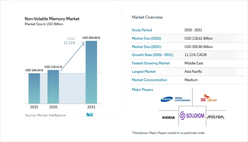
根據 Mordor Intelligence 預測,非揮發性記憶體市場規模將從 2025 年的 1056.4 億美元和 2026 年的 1186.1 億美元成長到 2031 年的 2008.5 億美元,2026 年至 2031 年的複合成長率為 11.1%。
本報告按記憶體類型(傳統非揮發性記憶體、新一代記憶體等)、終端用戶產業(家用電子電器、IT與通訊、其他)、介面(PCIe/NVMe、SATA、SPI/I2C、其他)、容量(256MB以下、512MB至1GB、2GB至4GB、8GB以上)、容量(256MB以下、512MB至1GB、2GB至4GB、8GB以上)、容量(企業儲存、其他產業自動化、其他區域和其他地區進行自動化、其他區域和區域進行自動化市場預測以美元計價。
全球非揮發性記憶體市場趨勢及洞察
資料中心的快速擴張正在推動對企業級非揮發性記憶體(NVM)的需求不斷成長。
超大規模資料中心業者計劃在2026年至2030年間部署100GW的新資料中心容量,每個機架都將整合Petabyte級全Flash陣列以處理推理工作負載。諸如美光9650等PCIe Gen 6固態硬碟的連續式讀取吞吐量可達28GB/s,彌合了運算和儲存吞吐量之間的差距。 NVIDIA的推理運算記憶體儲存平台將鍵值儲存從高頻寬記憶體卸載到企業級固態硬碟,在將擷取延遲保持在1毫秒以下的同時,將加速器成本降低了30%。這種轉變有利於三層單元(TLC)NAND閃存,其每天可承受三次寫入操作,非揮發性記憶體市場正日益凸顯其作為DRAM和物件儲存之間戰略緩衝的地位。隨著伺服器更新周期從五年縮短至三年,那些在韌體層級完善了耐久性最佳化的供應商正在與超大規模資料中心業者營運商簽訂長期合約。
汽車ADAS和車載資訊娛樂系統的普及
軟體定義車輛分配 2-4 TB 的儲存空間,用於儲存高解析度地圖、空中下載更新和感測器融合日誌。英飛凌的 SEMPER NOR 快閃記憶體已通過 ISO 26262 ASIL-D 安全認證,支援 L3 階自動駕駛的故障啟動架構。通用快閃記憶體 4.0 取代了傳統的嵌入式多媒體卡 (MMC),能夠以低功耗支援 4K影片串流傳輸。車規級 NAND 快閃記憶體必須能夠承受 -40 度C至 125 度C的溫度範圍和 3000 次寫入/擦除循環,因此價格比消費級模組高出 40%。隨著電氣系統從 12V 過渡到 48V,電壓瞬變變得更加頻繁,導致原始設備製造商 (OEM) 將片上糾錯碼 (ECC) 和斷電保護作為一項技術規範,這雖然增加了組件成本,但可以確保在再生煞車期間的資料完整性。
某些非揮發性記憶體架構的寫入耐久性較低
四層單元 (QLC) NAND 快閃記憶體的程式擦除循環次數僅 500 次,五層單元 (PLC) 為 200 次,而三層單元 (TLC) 則可達 3000 次。在資料庫日誌記錄和 AI查核點等寫入放大倍率超過 5 倍的應用中,QLC 快閃記憶體的壽命通常在 18 個月內就會耗盡。雖然機器學習控制器可以將壽命延長 40%,但額外 28% 的過度配置抵消了成本優勢。目前,超大規模資料中心業者正在調整其採購計劃,將 TLC 用於熱資料存儲,將 QLC 用於冷資料儲存。這種耐久性差距為 MRAM 和 ReRAM 在工業日誌記錄器和汽車黑盒子等領域創造了市場機會,因為這些應用的更換成本高於模組的初始價格。
細分市場分析
到2025年,快閃記憶體佔據了非揮發性記憶體市場63.78%的佔有率。儘管成本持續下降使其保持了主導地位,但預計到2031年,MRAM將以11.97%的複合年成長率成長。依賴快閃記憶體的非揮發性記憶體市場仍在擴張,但其壽命瓶頸在寫入密集型邊緣工作負載中日益凸顯。 64MB、128MB和256MB的MRAM已開始出貨,並應用於工業控制器、鐵路號誌系統和飛機黑盒子等領域。在韌體更新超出NAND快閃記憶體區塊擦除限制的情況下,這些MRAM已取代了NOR快閃記憶體。
第二代自旋軌道力矩技術正推動MRAM的密度向1Gb邁進,透過整合到28nm嵌入式邏輯中,可實現10ns的確定性寫入速度。鐵電RAM正被應用於RFID標籤,這些標籤需要10^14次循環的壽命,容量則限制在千位元組層級。 ReRAM和3D XPoint瞄準的是儲存層級記憶體層,但由於英特爾退出Optane業務,它們的商業化進程暫時停滯。如今,像Weebit Nano這樣的新創公司正致力於透過與代工廠合作來克服這項挑戰。這些趨勢表明,系統架構師正將高容量NAND快閃記憶體與位元組定址的MRAM結合,以平衡耐用性和成本,此設計將在預測期內重塑非揮發性記憶體市場。
到2025年,家用電子電器將佔總需求的44.81%,這主要得益於超過20億部智慧型手機、平板電腦和筆記型電腦的銷售成長。同時,受電動車銷量成長以及高級駕駛輔助系統(ADAS)對ASIL-D認證儲存設備的需求推動,汽車電子產業預計到2031年將維持11.56%的複合年成長率。隨著每個軟體定義平台整合10到20個配備256MB至4GB快閃記憶體的電控系統(ECU),汽車相關非揮發性記憶體的市場規模將大幅擴張。
由於高解析度地圖、無線更新和感測器日誌都快取在本地,因此與內燃機汽車相比,每台設備的非揮發性記憶體容量增加了八倍。通訊基礎設施佔企業級固態硬碟出貨量的28%,而在醫療歸檔領域,需要儲存10年的AES-256加密NAND快閃記憶體至關重要。工業自動化指定使用抗衝擊溫度低至-40 度C的NAND閃存,零售終端則使用UFS 3.1來縮短啟動時間。終端用戶的多樣化減輕了經濟波動的影響,即使智慧型手機的換代週期超過三年,對供應商的影響也得以降低。
區域分析
到2025年,亞太地區將佔非揮發性記憶體銷售額的46.11%,主要由三星、SK海力士、鎧俠和台灣晶圓代工廠推動。這些公司將供應全球75%的NAND快閃產能。韓國為龍仁工業叢集稅額扣抵,日本經濟產業省為美光廣島工廠提供5,000億日圓(約34億美元),預計該地區的複合年成長率將達到11.84%。中國正透過「長江儲存」加速推進國內NAND快閃記憶體的生產,但由於美國對極紫外線(EUV)光刻機的出口限制,128層節點以上的研發進程受阻。
到2025年,北美將佔據24%的市場佔有率,這主要得益於亞馬遜、微軟和谷歌的推動。它們總合部署的40EB企業級固態硬碟為長期採購提供了保障。 《晶片與科學法案》提供了527億美元的撥款,其中64.4億美元將用於美光在紐約州和愛達荷州的擴張,47.45億美元將用於三星在德克薩斯州的生產線,9.5億美元將用於SK海力士在印第安納州的封裝業務。歐洲的需求佔16%,德國一級汽車供應商從英飛凌和義法半導體採購符合ASIL-D標準的NAND快閃記憶體。
中東地區以12.25%的複合年成長率領先,這主要得益於政府對智慧城市和人工智慧(AI)服務資料中心基礎設施的337.9億美元投資。南美和非洲合計佔8%的市場佔有率,它們依靠基地台伺服器上的UFS隨身碟進行邊緣快取,以彌補骨幹網路頻寬的不足。儘管政府補貼緩解了區域集中度,但非揮發性記憶體市場仍然依賴東北亞的三個經濟體,其供應仍然容易受到地震、政治局勢和出口限制等事件的影響。
其他好處:
- Excel格式的市場預測(ME)表
- 3個月的分析師支持
目錄
第1章:引言
- 研究假設和市場定義
- 調查範圍
第2章:調查方法
第3章執行摘要
第4章 市場狀況
- 市場概覽
- 市場促進因素
- 資料中心的快速擴張正在推動對企業級非揮發性記憶體(NVM)的需求。
- 汽車ADAS和車載資訊娛樂系統的普及
- 需要持久、低延遲儲存的邊緣人工智慧工作負載
- 智慧型手機中UFS 4.0介面的主流化
- 基於3D-XPoint的持久性儲存模組的商業化
- 政府對國內半導體製造的優惠待遇
- 市場限制因素
- 某些非揮發性記憶體架構的寫入耐久性較差
- 高密度3D NAND堆疊中存在熱失控風險
- 對先進儲存節點的地緣政治出口限制
- 供求週期性導致價格波動
- 宏觀經濟因素對市場的影響
- 監理情勢
- 產業分析
- 波特五力分析
第5章 市場規模與成長預測
- 按記憶體類型
- 傳統非揮發性記憶體
- 快閃記憶體
- EEPROM
- SRAM
- EPROM
- 其他常規非揮發性記憶體
- 下一代非揮發性記憶體
- MRAM
- FRAM
- ReRAM
- 3D XPoint
- 奈米隨機存取記憶體
- 其他下一代非揮發性記憶體
- 傳統非揮發性記憶體
- 按最終用戶行業分類
- 家用電子產品
- 零售
- IT/通訊
- 衛生保健
- 其他終端用戶產業
- By Interface
- PCIe/NVMe
- SATA
- USB
- SPI/I2C
- 其他介面
- 按密度
- 256 MB 或更少
- 512 Mb~1 Gb
- 2 Gb~4 Gb
- 8 GB 或更多
- 透過使用
- 企業儲存
- 連網型設備和穿戴式裝置
- 工業自動化
- 汽車電子
- 其他用途
- 按地區
- 北美洲
- 美國
- 加拿大
- 其他北美國家
- 南美洲
- 巴西
- 阿根廷
- 其他南美國家
- 歐洲
- 英國
- 德國
- 法國
- 俄羅斯
- 其他歐洲國家
- 亞太地區
- 中國
- 日本
- 韓國
- 印度
- 其他亞太國家
- 中東
- 沙烏地阿拉伯
- 阿拉伯聯合大公國
- 土耳其
- 其他中東國家
- 非洲
- 南非
- 奈及利亞
- 其他非洲國家
- 北美洲
第6章 競爭情勢
- 市場集中度
- 策略趨勢
- 市佔率分析
- 公司簡介
- ROHM Co. Ltd
- STMicroelectronics NV
- Fujitsu Ltd
- Solidigm Inc.
- Honeywell International Inc.
- Micron Technology Inc.
- Samsung Electronics Co. Ltd
- Crossbar Inc.
- Infineon Technologies AG
- Avalanche Technology Inc.
- Western Digital Corp.
- SK Hynix Inc.
- Kioxia Holdings Corp.
- NXP Semiconductors NV
- Sony Semiconductor Solutions Corp.
- Seagate Technology Holdings PLC
- Renesas Electronics Corp.
- Intel Corporation
- GigaDevice Semiconductor Inc.
- Winbond Electronics Corp.
第7章 市場機會與未來展望
According to Mordor Intelligence, the non-volatile memory market size is projected to expand from USD 105.64 billion in 2025 and USD 118.61 billion in 2026 to USD 200.85 billion by 2031, registering a CAGR of 11.11% between 2026 and 2031.
This report is Segmented by Memory Type (Traditional Non-Volatile Memory, and Next-Generation and More), End-User Industry (Consumer Electronics, IT and Telecom, and More), Interface (PCIe/NVMe, SATA, SPI/I2C, and More), Density (<=256 Mb, 512 Mb-1 Gb, 2 Gb-4 Gb, and >=8 Gb), Application (Enterprise Storage, Industrial Automation, and More), and Geography. The Market Forecasts are Provided in Terms of Value (USD).
Global Non-Volatile Memory Market Trends and Insights
Exploding Data-Center Build-Outs Elevate Demand for Enterprise-Class NVM
Hyperscalers plan to deploy 100 GW of new data-center capacity between 2026 and 2030, and each rack integrates petabyte-scale all-flash arrays to serve inference workloads. PCIe Gen 6 solid-state drives, such as Micron's 9650, deliver 28 GB/s of sequential read throughput, closing the gap between compute and storage throughput. NVIDIA's Inference Compute Memory Storage Platform offloads key-value stores from high-bandwidth memory to enterprise SSDs, trimming accelerator costs by 30% while holding retrieval latency below one millisecond. This shift favors triple-level cell NAND that withstands 3 drive writes per day, elevating the non-volatile memory market as a strategic buffer between DRAM and object storage. As server refresh cycles accelerate from five to three years, suppliers that master firmware-level endurance optimization secure long-term contracts with hyperscalers.
Proliferation of Automotive ADAS and In-Vehicle Infotainment
Software-defined vehicles allocate 2-4 TB of storage for high-definition maps, over-the-air updates, and sensor-fusion logs. Infineon's SEMPER NOR Flash earned ASIL-D safety certification under ISO 26262, enabling fail-operational boot architectures in Level 3 autonomy. Universal Flash Storage 4.0 replaces legacy embedded MultiMediaCard to sustain 4K video streaming at lower power. Automotive-grade NAND must survive -40 °C to 125 °C and 3 000 program-erase cycles, commanding a 40% premium over consumer-grade modules. The transition from 12-V to 48-V electrical systems introduces voltage transients, prompting original equipment manufacturers to specify on-die error-correcting code and power-loss protection, boosting the bill of materials yet ensuring data integrity during regenerative braking.
Low Write-Endurance in Certain NVM Architectures
Quad-level cell NAND endures only 500 program-erase cycles and penta-level cell just 200, compared with 3 000 for triple-level cell. Database logging and AI checkpointing reach write amplification factors above 5, exhausting quad-level cell drives within 18 months. Machine-learning controllers extend life by 40% but add 28% over-provisioning, eroding cost advantages. Hyperscalers now reserve triple-level cells for hot data and relegate quad-level cells to cold storage, fragmenting procurement plans. The endurance gap opens white space for MRAM and ReRAM in industrial loggers and automotive black boxes, where replacement costs exceed initial module pricing.
Other drivers and restraints analyzed in the detailed report include:
- Edge AI Workloads Requiring Persistent, Low-Latency Storage
- Mainstream Adoption of UFS 4.0 Interface in Smartphones
- Thermal Runaway Risks in High-Density 3D NAND Stacks
For complete list of drivers and restraints, kindly check the Table Of Contents.
Segment Analysis
Flash memory accounted for 63.78% of the non-volatile memory market share in 2025. Steady cost declines sustained its dominance, yet MRAM is projected to grow at an 11.97% CAGR through 2031. The non-volatile memory market size tied to flash continues to expand, although write-heavy edge workloads expose endurance bottlenecks. MRAM shipments of 64 Mb, 128 Mb, and 256 Mb entered industrial controllers, railway signaling, and aviation black boxes, replacing NOR Flash where firmware updates exceed NAND's block-erase limitations.
Second-generation spin-orbit torque technology raises MRAM densities toward 1 Gb, and integration on 28 nm embedded logic yields deterministic 10 ns writes. Ferroelectric RAM services RFID tags that need 10^14 cycles but only kilobyte capacities. ReRAM and 3D XPoint aim for the storage-class memory tier, yet Intel's Optane exit created a commercialization pause that startups like Weebit Nano now aim to overcome through foundry alliances. These dynamics illustrate a pivot where system architects pair high-capacity NAND with byte-addressable MRAM to balance endurance and cost, a design that reshapes the non-volatile memory market over the forecast horizon.
Consumer electronics accounted for 44.81% of demand in 2025, driven by more than 2 billion smartphones, tablets, and laptops. Automotive electronics, however, is anticipated to post an 11.56% CAGR through 2031 as electric vehicle volumes rise and advanced driver-assistance systems require ASIL-D-certified storage. The non-volatile memory market size attributable to vehicles multiplies as each software-defined platform embeds 10-20 electronic control units with 256 MB to 4 GB flash.
High-definition maps, over-the-air updates, and sensor logs are cached locally, elevating per-vehicle non-volatile memory content eightfold relative to internal-combustion models. Telecommunications infrastructure accounts for 28% of enterprise SSD shipments, while healthcare archiving mandates AES-256-encrypted NAND with 10-year retention. Industrial automation specifies shock-resistant NAND rated to -40 °C, and retail terminals adopt UFS 3.1 to cut boot times. Diversified end users reduce cyclicality, insulating suppliers when smartphone refresh cycles extend beyond three years.
Geography Analysis
Asia-Pacific accounted for 46.11% of non-volatile memory revenue in 2025, led by Samsung, SK hynix, Kioxia, and Taiwanese foundries, which supply 75% of global NAND output. Regional growth is projected at an 11.84% CAGR as South Korea's 21.6 trillion won (USD 15.7 billion) tax credits finance the Yongin cluster, and Japan's Ministry of Economy, Trade and Industry grants JPY 500 billion (USD 3.4 billion) to Micron's Hiroshima fab. China accelerates domestic NAND at Yangtze Memory, but U.S. export controls on extreme-ultraviolet scanners stall progress beyond 128-layer nodes.
North America held 24% share in 2025, buoyed by Amazon, Microsoft, and Google, whose collective 40 EB of enterprise SSD deployments anchor long-term procurement. The CHIPS and Science Act unlocks USD 52.7 billion in subsidies, with USD 6.44 billion for Micron's New York and Idaho expansions, USD 4.745 billion for Samsung's Texas line, and USD 950 million for SK hynix packaging in Indiana. Europe captured 16% demand as Germany's automotive tier-ones source ASIL-D NAND from Infineon and STMicroelectronics.
The Middle East posts the fastest regional CAGR of 12.25%, driven by USD 33.79 billion in sovereign-wealth spending on data-center infrastructure for smart-city and artificial intelligence services. South America and Africa together account for 8% of the market and rely on edge caching to offset limited backbone bandwidth, using UFS packages in base-station servers. Government subsidies reduce geographic concentration, yet the non-volatile memory market still hinges on three Northeast Asian economies, leaving supply vulnerable to seismic, political, and export-control events.
- ROHM Co. Ltd
- STMicroelectronics NV
- Fujitsu Ltd
- Solidigm Inc.
- Honeywell International Inc.
- Micron Technology Inc.
- Samsung Electronics Co. Ltd
- Crossbar Inc.
- Infineon Technologies AG
- Avalanche Technology Inc.
- Western Digital Corp.
- SK Hynix Inc.
- Kioxia Holdings Corp.
- NXP Semiconductors NV
- Sony Semiconductor Solutions Corp.
- Seagate Technology Holdings PLC
- Renesas Electronics Corp.
- Intel Corporation
- GigaDevice Semiconductor Inc.
- Winbond Electronics Corp.
Additional Benefits:
- The market estimate (ME) sheet in Excel format
- 3 months of analyst support
TABLE OF CONTENTS
1 INTRODUCTION
- 1.1 Study Assumptions and Market Definition
- 1.2 Scope of the Study
2 RESEARCH METHODOLOGY
3 EXECUTIVE SUMMARY
4 MARKET LANDSCAPE
- 4.1 Market Overview
- 4.2 Market Drivers
- 4.2.1 Exploding Data-Center Build-Outs Elevate Demand for Enterprise-Class NVM
- 4.2.2 Proliferation of Automotive ADAS and In-Vehicle Infotainment
- 4.2.3 Edge AI Workloads Requiring Persistent, Low-Latency Storage
- 4.2.4 Mainstream Adoption of UFS 4.0 Interface in Smartphones
- 4.2.5 Commercialization of 3D-XPoint-Based Persistent Memory Modules
- 4.2.6 Government Incentives for Domestic Semiconductor Manufacturing
- 4.3 Market Restraints
- 4.3.1 Low Write-Endurance in Certain NVM Architectures
- 4.3.2 Thermal Runaway Risks in High-Density 3D NAND Stacks
- 4.3.3 Geopolitical Export Controls on Advanced Memory Nodes
- 4.3.4 Supply-Demand Cyclicality Causing Price Volatility
- 4.4 Impact of Macroeconomic Factors on the Market
- 4.5 Regulatory Landscape
- 4.6 Industrial Analysis
- 4.7 Porter's Five Forces Analysis
- 4.7.1 Threat of New Entrants
- 4.7.2 Bargaining Power of Buyers
- 4.7.3 Bargaining Power of Suppliers
- 4.7.4 Threat of Substitute Products
- 4.7.5 Intensity of Competitive Rivalry
5 MARKET SIZE AND GROWTH FORECASTS (VALUE)
- 5.1 By Memory Type
- 5.1.1 Traditional Non-Volatile Memory
- 5.1.1.1 Flash Memory
- 5.1.1.2 EEPROM
- 5.1.1.3 SRAM
- 5.1.1.4 EPROM
- 5.1.1.5 Rest of Traditional Non-Volatile Memory
- 5.1.2 Next-Generation Non-Volatile Memory
- 5.1.2.1 MRAM
- 5.1.2.2 FRAM
- 5.1.2.3 ReRAM
- 5.1.2.4 3D XPoint
- 5.1.2.5 Nano RAM
- 5.1.2.6 Rest of Next-Generation Non-Volatile Memory
- 5.1.1 Traditional Non-Volatile Memory
- 5.2 By End-User Industry
- 5.2.1 Consumer Electronics
- 5.2.2 Retail
- 5.2.3 IT and Telecom
- 5.2.4 Healthcare
- 5.2.5 Other End-User Industries
- 5.3 By Interface
- 5.3.1 PCIe/NVMe
- 5.3.2 SATA
- 5.3.3 USB
- 5.3.4 SPI/I2C
- 5.3.5 Other Interfaces
- 5.4 By Density
- 5.4.1 <=256 Mb
- 5.4.2 512 Mb-1 Gb
- 5.4.3 2 Gb-4 Gb
- 5.4.4 >=8 Gb
- 5.5 By Application
- 5.5.1 Enterprise Storage
- 5.5.2 Connected and Wearable Devices
- 5.5.3 Industrial Automation
- 5.5.4 Automotive Electronics
- 5.5.5 Rest of Applications
- 5.6 By Geography
- 5.6.1 North America
- 5.6.1.1 United States
- 5.6.1.2 Canada
- 5.6.1.3 Rest of North America
- 5.6.2 South America
- 5.6.2.1 Brazil
- 5.6.2.2 Argentina
- 5.6.2.3 Rest of South America
- 5.6.3 Europe
- 5.6.3.1 United Kingdom
- 5.6.3.2 Germany
- 5.6.3.3 France
- 5.6.3.4 Russia
- 5.6.3.5 Rest of Europe
- 5.6.4 Asia-Pacific
- 5.6.4.1 China
- 5.6.4.2 Japan
- 5.6.4.3 South Korea
- 5.6.4.4 India
- 5.6.4.5 Rest of Asia-Pacific
- 5.6.5 Middle East
- 5.6.5.1 Saudi Arabia
- 5.6.5.2 United Arab Emirates
- 5.6.5.3 Turkey
- 5.6.5.4 Rest of Middle East
- 5.6.6 Africa
- 5.6.6.1 South Africa
- 5.6.6.2 Nigeria
- 5.6.6.3 Rest of Africa
- 5.6.1 North America
6 COMPETITIVE LANDSCAPE
- 6.1 Market Concentration
- 6.2 Strategic Moves
- 6.3 Market Share Analysis
- 6.4 Company Profiles (includes Global Level Overview, Market Level Overview, Core Segments, Financials as available, Strategic Information, Market Rank/Share, Products and Services, Recent Developments)
- 6.4.1 ROHM Co. Ltd
- 6.4.2 STMicroelectronics NV
- 6.4.3 Fujitsu Ltd
- 6.4.4 Solidigm Inc.
- 6.4.5 Honeywell International Inc.
- 6.4.6 Micron Technology Inc.
- 6.4.7 Samsung Electronics Co. Ltd
- 6.4.8 Crossbar Inc.
- 6.4.9 Infineon Technologies AG
- 6.4.10 Avalanche Technology Inc.
- 6.4.11 Western Digital Corp.
- 6.4.12 SK Hynix Inc.
- 6.4.13 Kioxia Holdings Corp.
- 6.4.14 NXP Semiconductors NV
- 6.4.15 Sony Semiconductor Solutions Corp.
- 6.4.16 Seagate Technology Holdings PLC
- 6.4.17 Renesas Electronics Corp.
- 6.4.18 Intel Corporation
- 6.4.19 GigaDevice Semiconductor Inc.
- 6.4.20 Winbond Electronics Corp.
7 MARKET OPPORTUNITIES AND FUTURE OUTLOOK
- 7.1 White-Space and Unmet-Need Assessment
 非揮發性記憶體市場預測至2034年:按技術、應用、最終用戶和地區分類的全球分析
 NanoRAM市場:按儲存密度、外形規格和應用分類-2026-2032年全球市場預測
 非揮發性記憶體市場規模、佔有率、趨勢和預測:按類型、行業和地區分類,2026-2034 年非揮發性記憶體市場:2026-2032年全球市場預測(依記憶體類型、架構、介面、應用程式和最終用戶分類)
 非揮發性記憶體高速介面 (NVMe) - 2026 年全球交換矩陣市場報告
 光纖通道NVMe市場分析及預測(至2035年):按類型、產品、服務、技術、組件、應用、部署、最終用戶、解決方案和安裝類型分類
 全球NVMe(非揮發性記憶體高速介面)市場規模、佔有率、趨勢和成長分析報告(2026-2034年)全球非揮發性記憶體(NVM)市場規模、佔有率、趨勢和成長分析報告(2026-2034)2026年全球嵌入式非揮發性記憶體市場報告2026年全球非揮發性記憶體市場報告