


 |
市場調查報告書
商品編碼
2065536
晶片組:市場佔有率分析、行業趨勢和統計數據、成長預測(2026-2031)Chiplet - Market Share Analysis, Industry Trends & Statistics, Growth Forecasts (2026 - 2031) |
||||||
※ 本網頁內容可能與最新版本有所差異。詳細情況請與我們聯繫。
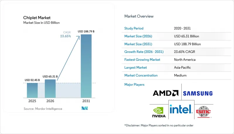
根據 Mordor Intelligence 預測,晶片市場規模預計將在 2025 年達到 524.5 億美元,2026 年達到 653.1 億美元,到 2031 年達到 1887.9 億美元,2026 年至 2031 年的複合年成長率為 23.65%。
本報告按處理器類型(中央處理器 (CPU)、圖形處理器 (GPU) 等)、終端用戶產業(資料中心和雲端運算、高效能運算、汽車和行動行程等)以及地區進行細分。市場預測以美元 (USD) 為單位。
全球晶片市場趨勢與洞察
克服人工智慧和高效能運算中的準星限制
晶片組市場的驅動力源自於一個簡單的事實:在最尖端科技,將大規模人工智慧和高效能運算處理器整合到單一單晶片上已不再現實。隨著運算需求的成長,多晶片整合技術使設計人員能夠在無需將所有功能都塞進一塊巨大的矽晶片的情況下,擴展邏輯、記憶體存取和I/O。因此,晶片組市場如今不僅與封裝創新緊密相關,也與藍圖息息相關。 2026年5月,AMD宣布其第六代EPYC Venice處理器已採用台積電2nm製程實現量產。這證實了基於晶片組的CPU設計仍然是通往下一代伺服器晶片的可靠途徑。此外,可重複使用的小型晶片也降低了企業投資完整系統晶片(SoC)專案的門檻,這進一步推動了晶片組市場的蓬勃發展。這些成本和良率優勢正在將晶片設計從高階選擇轉變為貫穿整個高階運算程式的核心產品策略。
採用 2.5D 和 3D 軟體包,主要是 HBM。
此外,人工智慧系統如今將算術邏輯和堆疊式記憶體整合到高密度封裝級設計中,這也推動了晶片市場的成長。事實上,這意味著先進封裝不再是輔助功能,而是成為裝置整體性能的核心。晶片市場正受益於這一轉變,因為封裝架構以及電晶體密度現在決定了頻寬、延遲和擴展效率。將於2025年8月發布的UCIe 3.0規範將支援的資料速率翻倍至48 GT/s和64 GT/s,擴展了邊帶傳輸距離,並增加了新的管理功能。這將有助於未來更輕鬆地適應要求更高的多晶片封裝設計。這項改進至關重要,因為記憶體和邏輯擴大在封裝層級被設計成一個整體單元,而不是在後續流程中單獨選擇。因此,晶片市場正朝著加速器設計人員、封裝專家和記憶體供應商之間更深入的合作開發方向發展。
高密度封裝中的散熱和供電瓶頸
隨著運算資源和記憶體日益整合於同一封裝尺寸內,晶片市場在溫度控管方面面臨明顯的技術限制。高密度 2.5D 和 3D 封裝設計產生的熱負荷,在大規模資料中心環境之外,難以透過標準冷卻方法有效應對。這直接限制了晶片市場的發展,因為即使晶片本身已準備就緒,部署也可能因此延遲。 2026 年 2 月發表於《Materials》雜誌的一項研究表明,針對基於晶片的異構封裝進行智慧熱最佳化,在 500 W/cm² 的條件下,可將熱阻降低 31%,壓降降低 42%,但仍依賴嵌入式微流體結構,而非傳統的冷卻方法。另一篇發表於 2025 年 7 月《Scientific Reports》雜誌的論文表明,2.5D 電源網路中的電熱協同最佳化可以將錯誤率降低到 4% 以下,但這也帶來了製造複雜性和成本顯著增加的挑戰。因此,雖然晶片組市場在超大規模環境中仍然最為強勁,但更廣泛的企業部署仍依賴卓越的溫度控管和電源解決方案。
細分市場分析
預計到2025年,CPU將佔據晶片組市場佔有率的34.54%,而AI加速器ASIC預計將以25.43%的複合年成長率成長至2031年。這一主導地位反映了現有伺服器CPU的龐大規模,以及基於晶片組的CPU佈局已在雲端和企業環境中得到驗證的事實。因此,晶片組市場目前依賴CPU作為短期收入來源,同時將AI ASIC作為未來成長的主要驅動力。 AMD正在推進的EPYC藍圖,包括計畫於2026年5月在台積電2nm製程上量產「Venice」處理器,也顯示尖端伺服器CPU在向下一代製程節點過渡的過程中仍將依賴晶片組細分。與全新的加速器類別相比,晶片組市場也受益於更低的部署風險,因為CPU平台為買家提供了一條熟悉的檢驗路徑。
由於超大規模資料中心業者不僅需要針對通用運算進行最佳化的晶片,還需要針對特定訓練和推理工作負載進行最佳化的晶片,人工智慧加速器專用積體電路(ASIC)的擴張正在加速。這推動晶片市場向客製化計算單元、專用內存配置以及針對每種部署場景的更精細的封裝級最佳化發展。雖然GPU在人工智慧訓練領域仍佔據很大一部分收入,但GPU、CPU、DPU、LPU和其他加速器之間的界線正變得越來越模糊。 NVIDIA的Vera Rubin平台將多種處理器類型整合到單一系統結構中,展示了異質整合如何模糊傳統處理器類型的界限。因此,晶片產業正從純粹的單一類別產品轉向混合處理器平台。
區域分析
到2025年,亞太地區將佔據晶片市場35.93%的佔有率,成為最大的區域中心。這一主導地位得益於台灣作為先進晶圓代工和封裝整合中心的持續領先地位,以及韓國在記憶體和封裝方面的關鍵能力。晶片市場也依賴亞太地區OSAT和基板生態系統的強大實力,該生態系統支援其他地區罕見的大規模生產。 AMD於2026年5月宣布將在台灣生產台積電的2nm「威尼斯」工藝,進一步鞏固了台灣作為先進伺服器晶片專案核心執行中心的地位。隨著區域供應鏈向先進節點製造方向發展,日本也透過設備、材料和封裝能力加強其在晶片市場的地位。根據SEAJ的預測,日本國內半導體設備市場預計在2026年成長22%,這顯示日本國內未來封裝和晶片製造能力的儲備正在不斷增強。
預計到2031年,北美將以26.41%的複合年成長率成長,成為晶片市場成長最快的地區。這一成長主要得益於超大規模資料中心業者、無晶圓廠半導體公司和先進系統設計公司的集中佈局,以及政策主導的國內半導體產能的投資。晶片市場在北美尤其活躍,因為許多定義人工智慧系統結構的公司都位於北美,儘管製造業務仍遍布亞太地區。 2026年3月,Ayar Labs宣布完成5億美元的E資金籌措,並將利用這筆資金加速共封裝光學元件的生產,並擴大在台灣的業務。這清楚地展現了北美作為設計和資本中心,與亞洲製造執行緊密相連的地位。同樣在2026年3月,NVIDIA和Marvell宣佈建立NVLink Fusion合作夥伴關係,凸顯了以客製化XPU、網路和光電核心的平台合作如何塑造北美晶片市場。
歐洲目前在晶片市場中所佔佔有率相對較小,但其重要性正隨著汽車、工業、航太和安全運算等領域的應用而日益凸顯。該地區的需求趨勢傾向於優先考慮經過驗證的、特定檢驗的多晶片解決方案,而不是單純追求出貨量。南美、中東和非洲仍是晶片市場的早期進入者,其需求主要與進口人工智慧基礎設施和雲端資料中心的建設有關。儘管這些地區目前規模仍然小規模,但隨著超大規模資料中心業者拓展業務範圍以及先進運算平台在更多終端市場普及,它們的市場佔有率將會不斷成長。
其他好處:
- Excel格式的市場預測(ME)表
- 3個月的分析師支持
目錄
第1章:引言
- 研究假設和市場定義
- 調查範圍
第2章:調查方法
第3章執行摘要
第4章 市場狀況
- 市場概覽
- 市場促進因素
- 利用人工智慧和高效能運算克服瞄準鏡限制
- 採用 2.5D/3D 軟體包,主要是 HBM。
- 透過 IP 重複使用降低高階節點中的非重複工程費用
- 5G、雲端運算和網路領域對解耦矽的需求。
- 用於擴充機架級人工智慧的光I/O晶片
- KGD測試與UCIe合作,降低通用晶片的風險
- 市場限制因素
- 高密度封裝中的散熱和供電瓶頸
- 供應商之間互通性不成熟以及與智慧財產權相關的風險
- KGD流量中的收益複利和測試成本通膨
- CoWoS、中介層、基板和光封裝瓶頸
- 產業價值鏈分析
- 監理情勢
- 技術展望
- 波特五力分析
第5章 市場規模與成長預測
- 依處理器類型
- 中央處理器(CPU)
- 圖形處理器(GPU)
- AI加速器ASIC
- 現場可程式閘陣列(FPGA)和自我調整晶片(SoC)
- 網路和資料處理單元(NPU/DPU)
- 其他基於晶片組的處理器類型
- 產品技術
- 2.5D中介層/橋接型封裝
- 3D堆疊/混合黏合包裝
- 基於扇出/RDL的先進封裝
- 採用有機基板的多晶片封裝
- 其他包裝技術
- 按最終用戶行業分類
- 資料中心和雲端運算
- 高效能運算
- 消費計算
- 汽車與出行
- 通訊與網路
- 工業和邊緣人工智慧
- 航太/國防
- 其他終端用戶產業
- 按地區
- 北美洲
- 美國
- 加拿大
- 墨西哥
- 歐洲
- 德國
- 英國
- 法國
- 義大利
- 其他歐洲國家
- 亞太地區
- 中國
- 日本
- 韓國
- 台灣
- 印度
- 其他亞太國家
- 南美洲
- 巴西
- 阿根廷
- 其他南美國家
- 中東和非洲
- 阿拉伯聯合大公國
- 沙烏地阿拉伯
- 南非
- 其他中東和非洲國家
- 北美洲
第6章 競爭情勢
- 市場集中度
- 策略趨勢
- Vendor Positioning Analysis
- 公司簡介
- Advanced Micro Devices, Inc.
- Intel Corporation
- NVIDIA Corporation
- Broadcom Inc.
- Marvell Technology, Inc.
- Taiwan Semiconductor Manufacturing Company Limited
- Samsung Electronics Co., Ltd.
- International Business Machines Corporation
- MediaTek Inc.
- Achronix Semiconductor Corporation
- Alphawave IP Group plc
- Ayar Labs, Inc.
- Rapidus Corporation
- Renesas Electronics
- Tenstorrent Holdings, Inc.
- SiFive, Inc.
第7章 市場機會與未來展望
According to Mordor Intelligence, the chiplet market size is projected to be USD 52.45 billion in 2025, USD 65.31 billion in 2026, and reach USD 188.79 billion by 2031, growing at a CAGR of 23.65% from 2026 to 2031.
This report is Segmented by Processor Type (Central Processing Units (CPUs), Graphics Processing Units (GPUs), and More), Packaging Technology (2. 5D Interposer/Bridge-Based Packaging, 3D Stacked/Hybrid-Bonded Packaging, and More), End-User Industry (Data Centers and Cloud Computing, High-Performance Computing, Automotive and Mobility, and More), and Geography. The Market Forecasts in Provided in Terms of Value (USD).
Global Chiplet Market Trends and Insights
AI And HPC Reticle-Limit Escape
The chiplet market is being pushed forward by the simple fact that very large AI and HPC processors are no longer practical as single monolithic dies at the leading edge. As compute demand rises, multi-die integration gives designers a way to scale logic, memory access, and I/O without forcing every function onto one oversized piece of silicon. This is why the chiplet market is now closely tied to the server CPU and AI accelerator road map, not just to packaging innovation. AMD said in May 2026 that its 6th Gen EPYC Venice processor entered production on TSMC 2nm technology, which confirms that chiplet-based CPU design remains the proven path into next-generation server silicon. The chiplet market also benefits because smaller reusable dies lower the economic barrier for companies that cannot fund a full leading-edge system-on-chip program. That cost and yield advantage is turning chiplet design from a high-end option into a core product strategy across advanced compute programs.
HBM-Centered 2.5D And 3D Package Adoption
The chiplet market is also being lifted by the way AI systems now combine compute logic with stacked memory in dense package-level designs. In practice, that means advanced packages are no longer a supporting feature, they are becoming the performance center of the full device. The chiplet market gains from this shift because package architecture now decides bandwidth, latency, and scaling efficiency as much as transistor density does. The UCIe 3.0 specification released in August 2025 doubled supported data rates to 48 GT/s and 64 GT/s, extended sideband reach, and added new manageability features, which makes more demanding multi-die package designs easier to support over time. That improvement matters because memory and logic are increasingly being designed together at package level rather than selected separately late in the process. As a result, the chiplet market is moving toward deeper co-development between accelerator designers, packaging specialists, and memory suppliers.
Thermal And Power-Delivery Bottlenecks In Dense Packages
The chiplet market faces a clear engineering limit in thermal management as more compute and memory are packed into the same footprint. Dense 2.5D and 3D package designs create heat loads that standard cooling approaches struggle to handle outside the largest data center environments. This is a direct restraint on the chiplet market because deployment can be delayed even when the silicon itself is ready for shipment. A February 2026 study in Materials showed that intelligent thermal optimization for chiplet-based heterogeneous packages improved thermal resistance by 31% and pressure drop by 42% at 500 W/cm2, but it still depended on embedded microfluidic structures rather than conventional cooling methods. A July 2025 paper in Scientific Reports also showed that electrothermal co-optimization in 2.5D power networks can cut error rates below 4%, though it adds significant manufacturing complexity and cost. The result is that the chiplet market remains strongest in hyperscale settings, while broader enterprise rollout still depends on better thermal and power-delivery solutions.
Other drivers and restraints analyzed in the detailed report include:
- Advanced-Node NRE Reduction Through IP Reuse
- 5G, Cloud, And Networking Demand For Disaggregated Silicon
- Immature Cross-Vendor Interoperability And IP Liability
For complete list of drivers and restraints, kindly check the Table Of Contents.
Segment Analysis
CPUs held 34.54% of chiplet market share in 2025, while AI accelerator ASICs are projected to grow at a 25.43% CAGR through 2031. That leadership reflects the scale of the existing server CPU base and the fact that chiplet-based CPU layouts are already proven in cloud and enterprise deployments. The chiplet market has therefore leaned on CPUs for near-term revenue while using AI ASICs as the main forward growth engine. AMD's continuing EPYC road map, including the May 2026 production ramp for Venice on TSMC 2nm, shows that advanced server CPUs still rely on chiplet partitioning to move into the next node generation. The chiplet market also benefits because CPU platforms give buyers a familiar validation path, which lowers adoption risk when compared with completely new accelerator categories.
AI accelerator ASICs are expanding faster because hyperscalers want silicon tuned for specific training and inference workloads rather than only general-purpose compute. That pushes the chiplet market toward custom compute tiles, specialized memory arrangements, and tighter package-level optimization for each deployment profile. GPUs still retain major revenue weight in AI training, yet the line between GPUs, CPUs, DPUs, LPUs, and other accelerators is becoming less distinct. NVIDIA's Vera Rubin platform combines multiple processor classes inside one system architecture, which shows how heterogeneous integration is blurring the old processor type boundaries. The chiplet industry is therefore moving toward mixed processor platforms rather than clean single-category products.
Geography Analysis
Asia-Pacific held 35.93% of chiplet market share in 2025, which made it the largest regional base for the chiplet market. The region leads because Taiwan remains central to advanced foundry output and package integration, while South Korea adds major memory and packaging capability. The chiplet market also depends on the depth of Asia-Pacific's OSAT and substrate ecosystem, which supports scale production in ways few other regions can match. AMD's May 2026 update on Venice production at TSMC 2nm reinforces Taiwan's role as the core execution hub for advanced server chip programs. Japan is strengthening its position in the chiplet market through equipment, materials, and packaging capacity as the regional supply chain moves deeper into advanced-node manufacturing. SEAJ projected that Japan's domestic semiconductor equipment market would grow 22% in fiscal 2026, which points to a stronger local pipeline for future packaging and chip fabrication capability.
North America is projected to expand at a 26.41% CAGR through 2031, making it the fastest-growing geography in the chiplet market. Growth is being driven by the concentration of hyperscalers, fabless chip companies, advanced system designers, and policy-led investment in domestic semiconductor capacity. The chiplet market is especially active in North America because many of the companies defining AI system architecture are based there, even when manufacturing still spans Asia-Pacific. Ayar Labs closed a USD 500 million Series E round in March 2026 and said it would use the funding to accelerate production of co-packaged optics and expand operations in Taiwan, which captures the region's role as a design and capital center connected to Asian manufacturing execution. The NVIDIA and Marvell NVLink Fusion partnership announced in March 2026 also highlights how the chiplet market in North America is being shaped by platform alliances around custom XPUs, networking, and photonics.
Europe holds a smaller position in the chiplet market, yet it is becoming more relevant through automotive, industrial, aerospace, and secure-compute use cases. The region's demand profile favors validated and application-specific multi-die solutions rather than sheer shipment scale. South America and the Middle East and Africa remain early-stage participants in the chiplet market, with demand tied mostly to imported AI infrastructure and cloud data center build-outs. These regions are still modest today, but they should become more visible as hyperscaler reach expands and advanced compute platforms spread into more end markets.
- Advanced Micro Devices, Inc.
- Intel Corporation
- NVIDIA Corporation
- Broadcom Inc.
- Marvell Technology, Inc.
- Taiwan Semiconductor Manufacturing Company Limited
- Samsung Electronics Co., Ltd.
- International Business Machines Corporation
- MediaTek Inc.
- Achronix Semiconductor Corporation
- Alphawave IP Group plc
- Ayar Labs, Inc.
- Rapidus Corporation
- Renesas Electronics
- Tenstorrent Holdings, Inc.
- SiFive, Inc.
Additional Benefits:
- The market estimate (ME) sheet in Excel format
- 3 months of analyst support
TABLE OF CONTENTS
1 INTRODUCTION
- 1.1 Study Assumptions and Market Definition
- 1.2 Scope of the Study
2 RESEARCH METHODOLOGY
3 EXECUTIVE SUMMARY
4 MARKET LANDSCAPE
- 4.1 Market Overview
- 4.2 Market Drivers
- 4.2.1 AI and HPC Reticle-limit Escape
- 4.2.2 Hbm-centered 2.5D/3D Package Adoption
- 4.2.3 Advanced-node NRE Reduction Through IP Reuse
- 4.2.4 5G, Cloud, and Networking Demand for Disaggregated Silicon
- 4.2.5 Optical I/O Chiplets for Rack-scale AI Scale-up
- 4.2.6 KGD Testing and UCIe Alliances De-risk Merchant Chiplets
- 4.3 Market Restraints
- 4.3.1 Thermal and Power-delivery Bottlenecks in Dense Packages
- 4.3.2 Immature Cross-vendor Interoperability and IP Liability
- 4.3.3 Yield Compounding and Test-cost Inflation in KGD Flows
- 4.3.4 CoWoS, Interposer, Substrate, and Optical-packaging Bottlenecks
- 4.4 Industry Value Chain Analysis
- 4.5 Regulatory Landscape
- 4.6 Technological Outlook
- 4.7 Porter's Five Forces Analysis
- 4.7.1 Bargaining Power of Suppliers
- 4.7.2 Bargaining Power of Buyers
- 4.7.3 Threat of New Entrants
- 4.7.4 Threat of Substitutes
- 4.7.5 Rivalry Among Competitors
5 MARKET SIZE AND GROWTH FORECASTS (VALUE)
- 5.1 By Processor Type
- 5.1.1 Central Processing Units (CPUs)
- 5.1.2 Graphics Processing Units (GPUs)
- 5.1.3 AI Accelerator ASICs
- 5.1.4 Field-Programmable Gate Arrays (FPGAs) and Adaptive SoCs
- 5.1.5 Networking and Data Processing Units (NPUs/DPUs)
- 5.1.6 Other Chiplet-Based Processor Types
- 5.2 By Packaging Technology
- 5.2.1 2.5D Interposer/Bridge-Based Packaging
- 5.2.2 3D Stacked/Hybrid-Bonded Packaging
- 5.2.3 Fan-Out/RDL-Based Advanced Packaging
- 5.2.4 Organic Substrate-Based Multi-Die Packaging
- 5.2.5 Other Packaging Technologies
- 5.3 By End-user Industry
- 5.3.1 Data Centers and Cloud Computing
- 5.3.2 High-Performance Computing
- 5.3.3 Consumer Computing
- 5.3.4 Automotive and Mobility
- 5.3.5 Telecommunications and Networking
- 5.3.6 Industrial and Edge AI
- 5.3.7 Aerospace and Defense
- 5.3.8 Other End-user Industries
- 5.4 By Geography
- 5.4.1 North America
- 5.4.1.1 United States
- 5.4.1.2 Canada
- 5.4.1.3 Mexico
- 5.4.2 Europe
- 5.4.2.1 Germany
- 5.4.2.2 United Kingdom
- 5.4.2.3 France
- 5.4.2.4 Italy
- 5.4.2.5 Rest of Europe
- 5.4.3 Asia-Pacific
- 5.4.3.1 China
- 5.4.3.2 Japan
- 5.4.3.3 South Korea
- 5.4.3.4 Taiwan
- 5.4.3.5 India
- 5.4.3.6 Rest of Asia-Pacific
- 5.4.4 South America
- 5.4.4.1 Brazil
- 5.4.4.2 Argentina
- 5.4.4.3 Rest of South America
- 5.4.5 Middle East and Africa
- 5.4.5.1 United Arab Emirates
- 5.4.5.2 Saudi Arabia
- 5.4.5.3 South Africa
- 5.4.5.4 Rest of Middle East and Africa
- 5.4.1 North America
6 COMPETITIVE LANDSCAPE
- 6.1 Market Concentration
- 6.2 Strategic Moves
- 6.3 Vendor Positioning Analysis
- 6.4 Company Profiles (includes Global Level Overview, Market Level Overview, Core Segments, Financials as available, Strategic Information, Market Rank/Share, Products and Services, Recent Developments)
- 6.4.1 Advanced Micro Devices, Inc.
- 6.4.2 Intel Corporation
- 6.4.3 NVIDIA Corporation
- 6.4.4 Broadcom Inc.
- 6.4.5 Marvell Technology, Inc.
- 6.4.6 Taiwan Semiconductor Manufacturing Company Limited
- 6.4.7 Samsung Electronics Co., Ltd.
- 6.4.8 International Business Machines Corporation
- 6.4.9 MediaTek Inc.
- 6.4.10 Achronix Semiconductor Corporation
- 6.4.11 Alphawave IP Group plc
- 6.4.12 Ayar Labs, Inc.
- 6.4.13 Rapidus Corporation
- 6.4.14 Renesas Electronics
- 6.4.15 Tenstorrent Holdings, Inc.
- 6.4.16 SiFive, Inc.
7 MARKET OPPORTUNITIES AND FUTURE OUTLOOK
- 7.1 White-Space and Unmet-Needs Assessment
 晶片整合解決方案市場分析及預測(至2035年):依類型、產品類型、服務、技術、組件、應用、材料類型、製程、最終用戶、解決方案分類
 Chiplet平台市場預測至2034年—按處理器類型、封裝技術、最終用戶和地區分類的全球分析晶片整合市場分析及至2035年預測:按類型、產品、服務、技術、應用和最終用戶分類晶片互連標準市場預測至2034年—按標準類型、互連技術、應用、最終用戶和地區分類的全球分析
 2026-2034年全球奈米晶片市場規模、佔有率、趨勢和成長分析報告
 Chiplet市場:2026年至2032年全球市場預測(依Chiplet類型、處理器類型、封裝技術、設計架構、構裝基板、應用、產業及最終用戶分類)
 晶片市場:按處理器類型、封裝技術和地區分類
 晶片互連市場機會、成長要素、產業趨勢分析及2026年至2035年預測Chiplets市場分析及預測至2035年:按類型、產品類型、技術、應用、材料類型、最終用戶、組件、功能、安裝類型、解決方案分類全球晶片技術市場:預測(至 2034 年)—按組件、互連類型、封裝技術、應用、最終用戶和地區進行分析