

 |
市場調查報告書
商品編碼
2065514
高速印刷電路板:市場佔有率分析、行業趨勢和統計數據以及成長預測(2026-2031 年)High-Speed PCB - Market Share Analysis, Industry Trends & Statistics, Growth Forecasts (2026 - 2031) |
||||||
※ 本網頁內容可能與最新版本有所差異。詳細情況請與我們聯繫。
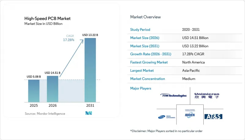
預計高速印刷電路板市場將從 2025 年的 50.8 億美元成長到 2026 年的 59.6 億美元,到 2031 年將進一步成長到 132.2 億美元,2026 年至 2031 年的複合年成長率為 17.28%。
本報告按PCB類型(12層及以上多層高速印刷電路板、HDI PCB等)、資料傳輸速度(最高25 Gbps、25–56 Gbps、56–112 Gbps、112 Gbps及以上)、材料類型(標準FR-4、中損耗材料等)、終端用戶(超大規模資料叢集、/ML/ML/ 服務供應商組。市場預測以美元(USD)計價。
全球高速印刷電路板市場趨勢及洞察
對人工智慧和機器學習GPU叢集的需求不斷成長
計畫於 2025 年推出的生成式人工智慧機架將整合超過 70 個 GPU,將總互連頻寬提升至 1Terabit/秒以上,同時保持 112 Gbps 的訊號完整性,並將 PCB 電流極限推至 1800 安培以上。超大規模資料中心業者所承擔的成本溢價是通用伺服器主機板的 3 到 4 倍,因為每一微秒的延遲都會直接影響大規模語言模型 (LLM)查詢的收入。資本預算支持長期供貨契約,使得掌握了焊盤內通孔 (VIA-IN-PAD) 高速互連 (HDI) 技術的製造商能夠確保多年大批量訂單的承諾。此外,設計複雜性的增加推高了不可重複設計成本 (NRE),進而提高了平均售價,擴大了高速印刷電路板市場的利潤空間。
快速採用 56-112 Gbps SerDes 和 PCIe 6.0
隨著 PCIe 6.0 於 2025 年推出,每通道頻寬將翻倍,但電壓裕度的降低意味著走線損耗(在 PCIe 4.0 中微不足道)如今已成為關鍵問題。為了維持 CPU 廠商設定的 36 分貝信噪比 (SNR)閾值,伺服器基板現在必須使用介電損耗角正切小於 0.002 的超低損耗環氧樹脂或 PTFE 層壓板。全球只有四家層壓板供應商能夠滿足這項標準,導致供應集中、前置作業時間長、價格飆升。設計公司越來越依賴3D電磁場模擬來最佳化短截線長度和背面鑽孔,從而增加了每個專案在工程工具上的支出。
超高數據速率下的溫度控管挑戰
一個以 112 Gbps 速率運行的 SerDes 通道,每個通道會散發超過 5 瓦的熱量,這意味著在一個 16 通道的設備中,80 瓦的熱量集中在不到 10 平方厘米的區域內,使基板溫度接近玻璃化轉變溫度極限。英特爾估計,目前基板級散熱解決方案的成本佔模組總成本的 22% 之多。浸沒式冷卻會改變介電常數,並使電阻變化高達 12 歐姆,這需要對走線形狀進行修正,並增加了設計的複雜性。因此,AI 伺服器的現場退貨率比傳統系統高出 40%,保固條款也隨之增加。
細分市場分析
至2025年,12層以上的多層基板將佔38%的銷售額,凸顯其作為雙路伺服器旗艦平台的地位。由於其在密度、成本和可製造性方面實現了平衡,能夠滿足56Gbps工作負載的需求,這些基板基板佔據了高速印刷電路板市場的最大佔有率。然而,隨著晶片組架構在加速器發展藍圖中的普及,基板PCB的複合年成長率(CAGR)正以18.28%的速度成長。隨著AMD、英特爾和英偉達將有機中介層以每模組150-200美元的價格投入量產,這些板式高速印刷電路板市場將進一步擴大。
基板的線寬和間距需求小於10微米,通孔密度超過10,000個/平方毫米,使其介於先進封裝和傳統PCB之間。為了滿足這項需求,AT&S和IBIDEN等製造商分別投資超過5億美元,在馬來西亞和日本推出新的生產線。雖然HDI基板在空間受限的邊緣伺服器中仍然很重要,但在儲存架構中,低串擾比微孔密度更為重要,因此背板仍然佔據主導地位。這種混合技術架構更有利於多元化供應商,而不是專注於單一領域的公司。
受 PCIe 5.0 和 100G 乙太網路引入的推動,設計用於 56–112 Gbps 連結的基板將在 2025 年佔據 41% 的銷售額。即便如此,112 Gbps 以上的細分市場預計將以 18.18% 的複合年成長率成長,成為高速印刷電路板市場成長最快的部分。高速印刷基板市場的擴張主要歸功於 PCIe 6.0 主機板和 800G 交換線路卡,它們要求在 30 吋走線上實現低於 30 分貝的插入損耗。
為了滿足這些要求,設計人員需要將過孔短截線縮短至 5 mil 以下,採用 ±3% 的控制電阻佈線公差,並過渡到 PTFE 或碳氫化合物層壓板。目前,一台 67 吉赫向量網路分析儀的價格高達 30 萬美元,因此對資本投資的需求很高,但如果沒有此類儀器,製造商就無法獲得超大規模認證。雖然速度較低、最高可達 25 Gbps 的基板在邊緣運算和小規模辦公室網路中仍然佔據主導地位,但隨著人工智慧推理的日益普及,收入正逐漸轉向更高數據速率的電路板。
區域分析
亞太地區憑藉著台灣、中國大陸、日本和韓國強大的製造能力,預計到2025年將佔全球銷售額的68%。這些國家在鑽孔、電鍍和組裝工藝方面擁有廣泛的生產能力,並集中在高度整合的園區內。該地區的供應商受益於規模經濟以及與層壓和銅箔生產設施的戰略性接近性。這種接近性有助於高速印刷電路板市場保持成本競爭力,尤其是在主流人工智慧伺服器應用領域。此外,研發中心集中在同一地點,能夠實現快速的製程創新和迭代,使該地區在競爭激烈的全球市場中擁有顯著優勢,能夠縮短產品上市時間。
儘管北美地區的產量較小,但卻是成長最快的地區,預計到2031年將以18.38%的複合年成長率成長。這主要得益於「主權運算」的需求,該需求要求在國內組裝以滿足國家安全工作負載的需求。諸如《晶片與科學法案》之類的項目正在推動對印刷電路板和半導體工廠的補貼,使得像TTM Technologies這樣的製造商能夠撥款1.5億美元用於擴建其位於紐約的超高速DI工廠。這種生產回流透過部分抵消供應鏈風險並縮短美國國防機構和雲端服務提供商的前置作業時間,擴大了該地區高速印刷電路板的市場佔有率。
在歐洲,重點依然放在高混合、高複雜度的產品。總部位於奧地利的AT&S及其德國工廠正在投資高價基板和玻璃芯基板,但與亞洲相比,其絕對產量仍然較低。南美、中東和非洲仍然是小眾市場,主要供應通訊和工業基板,而非人工智慧伺服器基板。總體而言,區域兩極化的趨勢正在加劇,產量集中在亞洲,而附加價值和韌性則集中在北美和部分歐洲工廠。
其他好處:
- Excel格式的市場預測(ME)表
- 3個月的分析師支持
目錄
第1章:引言
- 研究假設和市場定義
- 調查範圍
第2章:調查方法
第3章執行摘要
第4章 市場狀況
- 市場概覽
- 市場促進因素
- 資料中心對用於人工智慧和機器學習的GPU叢集的需求不斷成長
- 快速採用 56-112 Gbps SerDes 和 PCIe 6.0 標準
- 伺服器基板層數增加以及HDI的採用
- 擴大全球超大規模資料中心的容量
- 向晶片組架構過渡需要高速中介層
- 玻璃芯基板與SLB技術的出現
- 市場限制因素
- 超高速資料傳輸中的溫度控管挑戰
- 供應鏈中斷及材料前置作業時間
- 超低損耗層壓板製造的良率下降
- 對先進包裝設備出口的監管
- 宏觀經濟因素對市場的影響
- 產業價值鏈分析
- 監理情勢
- 技術展望
- 波特五力分析
第5章 市場規模與成長預測
- 依感測器類型
- 多層高速印刷電路基板(12層或以上)
- HDI PCBs
- 超低損耗/高頻PCB
- 背板PCB
- PCB (基板型PCB)
- 按資料傳輸速度
- 最高可達 25 Gbps
- 25~56 Gbps
- 56~112 Gbps
- 112 Gbps 或更高
- 材料類型
- 標準 FR-4
- 中損耗材料
- 低損耗材料
- 超低損耗材料
- 按最終用戶行業分類
- 超大規模資料中心(AI/ML叢集)
- 雲端服務供應商
- 企業級高效能運算
- 政府/研究機構
- 按地區
- 北美洲
- 美國
- 加拿大
- 墨西哥
- 南美洲
- 巴西
- 阿根廷
- 其他南美國家
- 歐洲
- 英國
- 德國
- 法國
- 義大利
- 其他歐洲國家
- 亞太地區
- 中國
- 日本
- 印度
- 韓國
- 其他亞太國家
- 中東和非洲
- 中東
- 阿拉伯聯合大公國
- 沙烏地阿拉伯
- 其他中東國家
- 非洲
- 南非
- 埃及
- 其他非洲國家
- 中東
- 北美洲
第6章 競爭情勢
- 市場集中度
- 策略趨勢
- 市佔率分析
- 公司簡介
- TTM Technologies Inc.
- Unimicron Technology Corp.
- Ibiden Co., Ltd.
- Samsung Electro-Mechanics Co., Ltd.
- AT&S Austria Technologie and Systemtechnik AG
- Compeq Manufacturing Co., Ltd.
- Nan Ya Printed Circuit Board Corp.
- Shennan Circuits Co., Ltd.
- Zhen Ding Technology Holding Limited
- Tripod Technology Corp.
- CMK Corporation
- Meiko Electronics Co., Ltd.
- WUS Printed Circuit Co., Ltd.
- Chin-Poon Industrial Co., Ltd.
- Sanmina Corporation
- Flex Ltd.(Multek)
- Kyocera Corporation
- RayMing Technology
- Advanced Circuits Inc.
- Shenzhen Kinwong Electronic Co., Ltd.
第7章 市場機會與未來展望
According to Mordor Intelligence, the high-speed PCB market size is expected to increase from USD 5.08 billion in 2025 to USD 5.96 billion in 2026 and to USD 13.22 billion by 2031, growing at a CAGR of 17.28% over 2026-2031.
This report is Segmented by PCB Type (Multilayer High-Speed PCBs 12+ Layers, HDI PCBs, and More), Data Rate Capability (Up To 25 Gbps, 25-56 Gbps, 56-112 Gbps, and 112 Gbps+), Material Type (Standard FR-4, Mid-Loss Materials, and More), End-Use Industry (Hyperscale Data Centers AI/ML Clusters, Cloud Service Providers, and More), and Geography. The Market Forecasts are Provided in Terms of Value (USD).
Global High-Speed PCB Market Trends and Insights
Growing Demand for AI and ML GPU Clusters
Generative AI racks introduced in 2025 integrate more than 70 GPUs and drive aggregate interconnect bandwidth above 1 terabit per second, pushing PCB current limits past 1,800 amperes while retaining 112 Gbps signal integrity. Hyperscalers absorb the three-to-four-fold cost premium over general-purpose server boards because every microsecond of latency directly affects revenue from large-language-model queries. Capital budgets support long-term supply agreements, so fabricators that master via-in-pad HDI techniques secure multi-year volume commitments. The design complexity also increases non-recurring engineering fees, which raise average selling prices and expand the high-speed PCB market profit pool.
Rapid Adoption of 56-112 Gbps SerDes and PCIe 6.0
The PCIe 6.0 rollout in 2025 doubles per-lane bandwidth but shrinks voltage margins, making trace losses that were minor at PCIe 4.0 now mission-critical. Server boards built on ultra-low-loss epoxy or PTFE laminates with dissipation factors below 0.002 are now required to sustain a 36 decibel signal-to-noise threshold set by CPU vendors. Only four laminate suppliers worldwide can meet this standard, so supply concentration extends lead times and hardens pricing. Design houses increasingly rely on 3-D electromagnetic simulation to optimize stub length and back-drilling, elevating engineering tool spend per project.
Thermal Management Challenges at Ultra-High Data Rates
SerDes channels operating at 112 Gbps dissipate more than 5 watts per lane, so a 16-lane device concentrates 80 watts over less than 10 cm2, driving board temperatures close to the glass-transition limit. Intel estimates that board-level cooling solutions now consume up to 22% of module costs. Immersion cooling alters dielectric constants, shifting impedance by up to 12 ohms, which forces trace-geometry compensation and raises design complexity. Resulting field-return rates for AI servers run 40% higher than traditional systems, inflating warranty reserves.
Other drivers and restraints analyzed in the detailed report include:
- Increasing Layer Counts and HDI Adoption
- Expansion of Hyperscale Data Center Capacity
- Supply Chain Disruptions and Material Lead Times
For complete list of drivers and restraints, kindly check the Table Of Contents.
Segment Analysis
Multilayer boards with 12 or more layers accounted for 38% of revenue in 2025, underscoring their role as the workhorse platform for dual-socket servers. These boards account for the largest slice of the high-speed PCB market share because they balance density, cost, and manufacturability for 56 Gbps workloads. Substrate-like PCBs, however, are climbing at an 18.28% CAGR as chiplet architectures propagate across accelerator roadmaps. The high-speed PCB market for these substrate-like formats will grow as AMD, Intel, and NVIDIA bring organic interposers priced at USD 150-200 per module into production.
Substrate-like boards demand line-and-space below 10 microns and via densities over 10,000 vias/mm2, positioning them halfway between advanced packaging and traditional PCB realms. Fabricators such as AT&S and Ibiden channel more than USD 500 million each into new Malaysian and Japanese lines to address this demand. HDI boards retain relevance in edge servers where space is scarce, while backplanes continue to dominate storage fabrics that prize low-crosstalk over micro-via density. This mixed technology stack favors diversified suppliers rather than single-niche shops.
Boards engineered for 56-112 Gbps links secured 41% of 2025 revenue, powered by PCIe 5.0 and 100G Ethernet deployments. Even so, the 112 Gbps-plus cohort is projected to rise at an 18.18% CAGR, making it the fastest contributor to overall high-speed PCB market growth. High-speed printed circuit board market size gains in this category reflect PCIe 6.0 motherboards and 800G switch line cards that require insertion losses below 30 decibels across 30-inch traces.
Meeting these budgets obliges designers to shorten via stubs below 5 mils, adopt controlled-impedance routing tolerances of +-3%, and shift to PTFE or hydrocarbon-based laminates. Capital needs escalate because a single 67 gigahertz vector network analyzer now costs USD 300,000, yet without such metrology, fabricators cannot win hyperscale qualifications. Lower-speed boards up to 25 Gbps remain prevalent in edge compute and small-office networking, but revenue gradually gravitates toward the higher data-rate tiers as AI inference proliferates.
Geography Analysis
Asia-Pacific accounted for 68% of 2025 sales, driven by the robust manufacturing capabilities of Taiwan, China, Japan, and South Korea. These countries host extensive capacities across drilling, plating, and assembly processes, consolidated within highly integrated campuses. The region's vendors benefit significantly from economies of scale and their strategic proximity to laminate and copper-foil production facilities. This proximity ensures the high-speed PCB market remains cost-competitive, particularly for mainstream AI server applications. Additionally, the presence of co-located research and development centers fosters rapid process innovation and iteration, providing the region with a critical time-to-market advantage in a highly competitive global market.
North America, though smaller in volume, is the fastest-growing region, with a 18.38% CAGR through 2031, driven by sovereign-compute mandates requiring domestic assembly for national-security workloads. Programs such as the CHIPS and Science Act steer subsidies toward PCB and semiconductor facilities, so fabricators like TTM Technologies earmark USD 150 million for ultra-HDI expansion in New York. This reshoring partially offsets supply-chain risk and shortens lead times for U.S. defense and cloud operators, enlarging the regional high-speed PCB market share.
Europe keeps a high-mix, high-complexity focus. Austria-based AT&S and Germany-based sites invest in substrate-like and glass-core boards that command premium pricing, though absolute volumes remain modest compared with Asia. South America, the Middle East, and Africa remain niche, supplying telecom and industrial boards rather than AI servers. Overall, a bifurcated geography emerges, with volume tilting toward Asia while value and resilience tilt toward North America and select European plants.
- TTM Technologies Inc.
- Unimicron Technology Corp.
- Ibiden Co., Ltd.
- Samsung Electro-Mechanics Co., Ltd.
- AT&S Austria Technologie and Systemtechnik AG
- Compeq Manufacturing Co., Ltd.
- Nan Ya Printed Circuit Board Corp.
- Shennan Circuits Co., Ltd.
- Zhen Ding Technology Holding Limited
- Tripod Technology Corp.
- CMK Corporation
- Meiko Electronics Co., Ltd.
- WUS Printed Circuit Co., Ltd.
- Chin-Poon Industrial Co., Ltd.
- Sanmina Corporation
- Flex Ltd. (Multek)
- Kyocera Corporation
- RayMing Technology
- Advanced Circuits Inc.
- Shenzhen Kinwong Electronic Co., Ltd.
Additional Benefits:
- The market estimate (ME) sheet in Excel format
- 3 months of analyst support
TABLE OF CONTENTS
1 INTRODUCTION
- 1.1 Study Assumptions and Market Definition
- 1.2 Scope of the Study
2 RESEARCH METHODOLOGY
3 EXECUTIVE SUMMARY
4 MARKET LANDSCAPE
- 4.1 Market Overview
- 4.2 Market Drivers
- 4.2.1 Growing Demand for AI and ML GPU Clusters in Data Centers
- 4.2.2 Rapid Adoption of 56-112 Gbps SerDes and PCIe 6.0 Standards
- 4.2.3 Increasing Layer Counts and HDI Adoption in Server Boards
- 4.2.4 Expansion of Hyperscale Data Center Capacity Worldwide
- 4.2.5 Transition to Chiplet Architectures Requiring High-Speed Interposers
- 4.2.6 Emergence of Glass Core Substrates and SLB Technology
- 4.3 Market Restraints
- 4.3.1 Thermal Management Challenges at Ultra-High Data Rates
- 4.3.2 Supply Chain Disruptions and Material Lead Times
- 4.3.3 Yield Losses in Ultra-Low-Loss Laminate Fabrication
- 4.3.4 Regulatory Scrutiny on Export of Advanced Packaging Equipment
- 4.4 Impact of Macroeconomic Factors on the Market
- 4.5 Industry Value Chain Analysis
- 4.6 Regulatory Landscape
- 4.7 Technological Outlook
- 4.8 Porter's Five Forces Analysis
- 4.8.1 Bargaining Power of Suppliers
- 4.8.2 Bargaining Power of Buyers
- 4.8.3 Threat of New Entrants
- 4.8.4 Threat of Substitutes
- 4.8.5 Intensity iof Competitive Rivalry
5 MARKET SIZE AND GROWTH FORECASTS (VALUE)
- 5.1 By Sensor Type
- 5.1.1 Multilayer High-Speed PCBs (12+ Layers)
- 5.1.2 HDI PCBs
- 5.1.3 Ultra-Low-Loss / High-Frequency PCBs
- 5.1.4 Backplane PCBs
- 5.1.5 Substrate-Like PCBs
- 5.2 By Data Rate Capability
- 5.2.1 Up to 25 Gbps
- 5.2.2 25-56 Gbps
- 5.2.3 56-112 Gbps
- 5.2.4 112 Gbps+
- 5.3 By Material Type
- 5.3.1 Standard FR-4
- 5.3.2 Mid-Loss Materials
- 5.3.3 Low-Loss Materials
- 5.3.4 Ultra-Low-Loss Materials
- 5.4 By End-User Industry
- 5.4.1 Hyperscale Data Centers (AI/ML Clusters)
- 5.4.2 Cloud Service Providers
- 5.4.3 Enterprise HPC
- 5.4.4 Government / Research Labs
- 5.5 By Geography
- 5.5.1 North America
- 5.5.1.1 United States
- 5.5.1.2 Canada
- 5.5.1.3 Mexico
- 5.5.2 South America
- 5.5.2.1 Brazil
- 5.5.2.2 Argentina
- 5.5.2.3 Rest of South America
- 5.5.3 Europe
- 5.5.3.1 United Kingdom
- 5.5.3.2 Germany
- 5.5.3.3 France
- 5.5.3.4 Italy
- 5.5.3.5 Rest of Europe
- 5.5.4 Asia-Pacific
- 5.5.4.1 China
- 5.5.4.2 Japan
- 5.5.4.3 India
- 5.5.4.4 South Korea
- 5.5.4.5 Rest of Asia-Pacific
- 5.5.5 Middle East and Africa
- 5.5.5.1 Middle East
- 5.5.5.1.1 United Arab Emirates
- 5.5.5.1.2 Saudi Arabia
- 5.5.5.1.3 Rest of Middle East
- 5.5.5.2 Africa
- 5.5.5.2.1 South Africa
- 5.5.5.2.2 Egypt
- 5.5.5.2.3 Rest of Africa
- 5.5.5.1 Middle East
- 5.5.1 North America
6 COMPETITIVE LANDSCAPE
- 6.1 Market Concentration
- 6.2 Strategic Moves
- 6.3 Market Share Analysis
- 6.4 Company Profiles (includes Global Level Overview, Market Level Overview, Core Segments, Financials as available, Strategic Information, Market Rank/Share, Products and Services, Recent Developments)
- 6.4.1 TTM Technologies Inc.
- 6.4.2 Unimicron Technology Corp.
- 6.4.3 Ibiden Co., Ltd.
- 6.4.4 Samsung Electro-Mechanics Co., Ltd.
- 6.4.5 AT&S Austria Technologie and Systemtechnik AG
- 6.4.6 Compeq Manufacturing Co., Ltd.
- 6.4.7 Nan Ya Printed Circuit Board Corp.
- 6.4.8 Shennan Circuits Co., Ltd.
- 6.4.9 Zhen Ding Technology Holding Limited
- 6.4.10 Tripod Technology Corp.
- 6.4.11 CMK Corporation
- 6.4.12 Meiko Electronics Co., Ltd.
- 6.4.13 WUS Printed Circuit Co., Ltd.
- 6.4.14 Chin-Poon Industrial Co., Ltd.
- 6.4.15 Sanmina Corporation
- 6.4.16 Flex Ltd. (Multek)
- 6.4.17 Kyocera Corporation
- 6.4.18 RayMing Technology
- 6.4.19 Advanced Circuits Inc.
- 6.4.20 Shenzhen Kinwong Electronic Co., Ltd.
7 MARKET OPPORTUNITIES AND FUTURE OUTLOOK
- 7.1 White-Space and Unmet-Need Assessment
