

 |
市場調查報告書
商品編碼
2065512
EUV光阻劑材質:市場佔有率分析、產業趨勢與統計資料、成長預測(2026-2031年)EUV Photoresist Materials - Market Share Analysis, Industry Trends & Statistics, Growth Forecasts (2026 - 2031) |
||||||
※ 本網頁內容可能與最新版本有所差異。詳細情況請與我們聯繫。
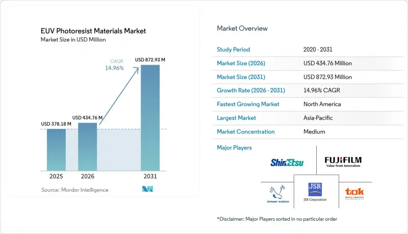
根據 Mordor Intelligence 預測,eUV光阻劑材料市場規模將從 2025 年的 3.7818 億美元和 2026 年的 4.3476 億美元成長到 2031 年的 8.7293 億美元,2026 年至 2031 年的年複合成長率(CAGR)率為 14.96%。
本報告按抗蝕劑類型(化學放大抗蝕劑、金屬氧化物抗蝕劑、非化學放大光阻和乾法抗蝕劑)、節點相容性(最先進的3nm以下節點和先進的5nm-7nm節點)、終端客戶類型(純晶圓代工廠和整合裝置製造商)以及地區(北美、歐洲、亞太地區和世界其他地區)進行細分。市場預測以美元計價。
全球EUV光阻劑材料市場趨勢及洞察
EUV製程在3奈米以下節點迅速普及
從浸沒式深紫外線 (DUV) 多重圖形化到單一途徑極紫外線 (EUV) 微影的轉變,正在克服先進微結構解析度的限制。台積電目前在其 2 奈米製程中使用 EUV 技術進行 20 層以上的圖形化,幾乎是其 3 奈米製程曝光層數的兩倍,從而減少了光罩總數和製程步驟。英特爾推出了高數值孔徑 (NA) 設備,實現了 8 奈米解析度,從而能夠進行單程圖形化,提高良率並顯著降低缺陷密度。三星的第二代 2 奈米技術透過最佳化抗蝕劑,將線邊緣粗糙度降低到 1.5 奈米以下,實現了 70% 的良率。雖然每台高 NA 掃描儀的成本約為 3.5 億美元,但晶圓廠可以透過消除多重圖形化循環和縮短週期時間來彌補這部分成本。
擴大人工智慧加速器的晶圓廠產能
到2025年,人工智慧(AI)晶片將佔據3奈米晶圓配額的大部分,前置作業時間將超過50週。光是英偉達就將在2026年獲得台積電一半以上的先進封裝產能,這將推動晶圓和封裝層面極紫外(EUV)光阻劑材料需求的激增。亞利桑那州、泰勒市和俄亥俄州的產能擴張得到了《晶片法案》(CHIPS Act)下總合192億美元的津貼和貸款支持,訂單在晶圓廠全面運作之前,抗蝕劑也已加速成長。由於每台高數值孔徑(NA)掃描儀每年消耗價值200萬至300萬美元的光阻劑,設備的增加將直接導致材料消耗量的增加。
EUV掃描器供不應求
ASML計劃在2025年交付60套系統,2027年交付超過80套系統,但代工廠的訂單訂單已持續兩年之久。每次交付延遲都會導致晶圓廠每月減少多達15,000片晶圓的產量,迫使業者限制光阻劑的採購,並影響EUV光阻劑材料市場的收入。英特爾俄亥俄州工廠專案延誤七年的主要原因是高數值孔徑(NA)設備的交付週期長、交貨期長,凸顯了設備供應壟斷如何阻礙區域多元化。短期供不應求進一步提升了金屬氧化物抗蝕劑和乾式抗蝕劑的提案,因為它們可以提高劑量效率並增加單機產能。
細分市場分析
以氧化錫叢集技術為核心的金屬氧化物抗蝕劑預計將成為成長最強勁的市場,到2031年複合年成長率將達到18.4%。截至2025年,化學放大光阻產品仍主導極紫外光光阻劑材料市場,因為晶圓廠優先考慮的是已驗證的線路相容性和正性極性。 2026年,隨著Lam Research公司展示其氣相「Aether」平台,市場應用趨勢轉變。該平台可將化學品消耗量減少高達25%,並實現小於20奈米的單次印刷圖案。
儘管化學放大抗蝕劑仍具有規模經濟優勢,但3奈米以下節點的隨機缺陷迫使晶圓廠嘗試其他化學技術。 JSR和Lam Research目前提供了一種混合工作流程,將氣相沉積與無機光敏材料相結合,為正性金屬氧化物解決方案鋪平了道路,這些解決方案預計將在預測期內取代現有的聚合物基產品。美國環保署(EPA)和歐洲化學品管理局(ECHA)對PFAS含量的限制措施正在加速這項轉型,並鼓勵供應商轉向不含PFAS的金屬氧化物和乾粉配方。
區域分析
在北美,《晶片創新與生產法案》(CHIPS Act)的獎勵正在加速推進三個大型晶圓廠項目——台積電亞利桑那工廠、三星泰勒工廠和英特爾俄亥俄工廠——預計2026年至2031年間的複合年成長率將達到19.2%,位居行業之首。這些工廠一旦運作,每月將新增超過40萬片總合晶圓的產量,使EUV光阻劑材料的年需求量增加1.5億至2億美元。限制在光阻劑中使用全氟烷基和多氟烷基物質(PFAS)的法規將消除合規的模糊之處,並促進本地材料生產。
預計到2025年,亞太地區將佔據37.7%的市場佔有率,並繼續保持其營收支柱地位。這主要得益於台灣和韓國擁有全球超過60%的極紫外光微影掃描器。當地供應商受益於較短的物流路線,而日本化學企業則在平澤和茨城擴大生產規模,以利用其與三星和台積電的地理接近性。儘管亞太地區保持領先地位,但隨著北美產能的擴張,其市佔率成長速度預計將會放緩。
儘管歐洲在絕對規模上落後於其他國家,但它正受益於總額達430億歐元的《歐洲晶片法案》,該法案旨在2030年將該地區半導體市場佔有率翻倍。 Imec位於魯汶的工廠和附近的JSR製造地是未來在德國和法國建造的高數值孔徑節點的材料認證中心。隨著提案的REACH附件十五明確了允許的PFAS含量閾值,並為批准擴大產能提供了必要的監管確定性,供應商的興趣日益濃厚。
其他好處:
- Excel格式的市場預測(ME)表
- 3個月的分析師支持
目錄
第1章:引言
- 研究假設和市場定義
- 調查範圍
第2章:調查方法
第3章執行摘要
第4章 市場狀況
- 市場概覽
- 市場促進因素
- 快速引入3奈米節點的極紫外光刻技術
- 專業代工廠在尖端邏輯領域的優勢
- 擴大我們人工智慧加速器工廠的產能。
- 政府對國內先進節點的補貼
- 促進供應鏈本地化的措施(CHIPS、K-CHIP 等)
- 利用金屬氧化物乾式抗蝕劑提高良率
- 市場限制因素
- 與線邊緣粗糙度為 3 奈米或更低相關的挑戰
- EUV掃描器供不應求
- MOR化學品的環境、健康與安全問題
- 與浸沒式深紫外光相比,CoO較高
- 產業價值鏈分析
- 監理情勢
- 技術展望
- 宏觀經濟因素對市場的影響
- 波特五力分析
第5章 市場規模與成長預測
- 依抗蝕劑類型
- 化學敏化抗蝕劑(CAR)
- 金屬氧化物抗蝕劑(MOR)
- 非化學感光/乾式抗蝕劑
- 節點相容性
- 尖端技術(3奈米或更小)
- 先進節點(5奈米至7奈米)
- 最終用戶
- 專業鑄造廠
- 垂直整合設備製造商 (IDM)
- 按地區
- 北美洲
- 美國
- 加拿大
- 墨西哥
- 歐洲
- 英國
- 德國
- 法國
- 義大利
- 其他歐洲國家
- 亞太地區
- 中國
- 日本
- 印度
- 韓國
- 其他亞太國家
- 世界其他地區
- 北美洲
第6章 競爭情勢
- 市場集中度
- 策略趨勢
- 市佔率分析
- 公司簡介
- JSR Corporation
- Tokyo Ohka Kogyo Co., Ltd.(TOK)
- Fujifilm Holdings Corporation
- Shin-Etsu Chemical Co., Ltd.
- Brewer Science, Inc.
- Inpria Corporation(JSR)
- Merck KGaA(AZ Electronic Materials)
- DuPont de Nemours, Inc.
- Sumitomo Chemical Co., Ltd.
- Dongjin Semichem Co., Ltd.
- Avantama AG
- Lam Research Corporation
- LG Chem Ltd.
- Arkema SA
- Tokyo Electron Limited(dry resist co-development)
- S&S Tech Corporation
- Kayaku Advanced Materials, Inc.
- GlobalWafers Co., Ltd.
- Integrated Micro Materials LLC
- Beijing Institute of Chemical Engineering(BICEM)
第7章 市場機會與未來展望
According to Mordor Intelligence, the eUV photoresist materials market size is projected to expand from USD 378.18 million in 2025 and USD 434.76 million in 2026 to USD 872.93 million by 2031, registering a CAGR of 14.96% between 2026 and 2031.
This report is Segmented by Resist Type (Chemically Amplified Resists, Metal Oxide Resists, and Non-Chemically Amplified and Dry Resists), Node Compatibility (Leading Edge 3 Nm and Below, and Advanced Nodes 5 Nm To 7 Nm), End Customer Type (Pure-Play Foundries, and IDMs), and Geography (North America, Europe, Asia-Pacific, and Rest of the World). Market Forecasts are Provided in Terms of Value (USD).
Global EUV Photoresist Materials Market Trends and Insights
Rapid EUV Adoption For <=3 Nm Nodes
The migration from immersion deep-ultraviolet multi-patterning to single-pass extreme-ultraviolet exposure eliminates resolution ceilings at advanced geometries. TSMC now patterns more than 20 layers with EUV on its 2-nanometer process, almost twice the count used at 3-nanometer, which reduces total masks and process steps.Intel integrates high-NA tools that achieve 8-nanometer resolution, enabling single-exposure patterning that boosts yield and slashes defect density. Samsung's second-generation 2-nanometer technology reached 70% yields after resist optimizations cut line-edge roughness below 1.5 nanometers. Although each high-NA scanner costs about USD 350 million, fabs recover the differential by eliminating multi-patterning loops and realizing faster cycle times.
Expansion Of AI Accelerator Fab Capacity
Artificial-intelligence chips consumed most 3-nanometer wafer allocations in 2025, stretching lead times past 50 weeks. NVIDIA alone booked more than half of TSMC's advanced packaging output in 2026, swelling demand for EUV photoresist materials market volumes at both wafer and package levels. Capacity additions in Arizona, Taylor, and Ohio, backed by USD 19.2 billion in combined CHIPS Act grants and loans, pull forward resist orders even before the fabs are fully ramped. With every high-NA scanner absorbing USD 2-3 million of photoresist a year, incremental tool deployments translate directly into material consumption.
Limited EUV Scanner Availability
ASML shipped 60 systems in 2025 and plans just over 80 in 2027, yet foundry order books stretch two years ahead. Each delay deprives a fab of up to 15,000 wafers per month, forcing operators to ration photoresist purchases and injecting revenue volatility into the EUV photoresist materials market. Intel's Ohio complex slipped seven years primarily because of long-cycle high-NA tool deliveries, underscoring how monopoly equipment supply throttles regional diversification. Short-term shortages also amplify the value proposition of metal oxide and dry resists, which raise dose efficiency and stretch throughput per tool.
Other drivers and restraints analyzed in the detailed report include:
- Dominance Of Pure-Play Foundries In Leading-Edge Logic
- Government Subsidies For On-Shore Advanced Nodes
- Line Edge Roughness Challenges Below 3 Nm
For complete list of drivers and restraints, kindly check the Table Of Contents.
Segment Analysis
Metal oxide resists, anchored by tin-oxide cluster technology, are projected to register the strongest growth, advancing at an 18.4% CAGR through 2031. In 2025, chemically amplified products still dominated the EUV photoresist materials market size because fabs favor proven track compatibility and positive-tone polarity. Adoption momentum shifted in 2026 when Lam Research demonstrated its vapor-phase Aether platform that cuts chemical consumption by up to 25% and achieves single-print patterns below 20 nanometers.
Chemically amplified resists retain economies of scale, yet stochastic defects at sub-3-nanometer nodes compel fabs to pilot alternative chemistries. JSR and Lam Research now offer hybrid workflows that pair vapor deposition with inorganic photosensitizers, signaling a path toward positive-tone metal oxide solutions that could displace polymer incumbents within the forecast horizon. Regulatory moves by the U.S. Environmental Protection Agency and the European Chemicals Agency accelerate this pivot by capping PFAS content, incentivizing suppliers to transition to PFAS-free metal oxide and dry formulations.
Geography Analysis
North America is projected to record the fastest CAGR at 19.2% during 2026-2031 as CHIPS Act incentives accelerate three mega-fab projects: TSMC Arizona, Samsung Taylor, and Intel Ohio. Once operational, these plants will collectively add more than 400,000 leading-edge wafer starts per month, translating into an additional USD 150-200 million in annual demand for EUV photoresist materials market volumes. Regulations that establish a controlled-use pathway for PFAS in photoresists reduce compliance ambiguity and encourage local production of materials.
Asia-Pacific remains the revenue anchor, with a 37.7% share in 2025, as Taiwan and South Korea host more than 60% of the global EUV scanner fleet. Local suppliers benefit from short logistics lanes, while Japanese chemical companies are expanding production in Pyeongtaek and Ibaraki to co-locate with Samsung and TSMC. Although the region maintains its leadership, incremental share gains are likely to moderate as North American capacity scales.
Europe trails in absolute size but benefits from the EUR 43 billion European Chips Act, which aims to double the regional semiconductor share by 2030. Imec's Leuven hub and JSR's nearby manufacturing base serve as material qualification centers for future high-NA nodes built in Germany and France. Supplier interest is rising because the REACH Annex XV proposal clarifies permissible PFAS thresholds, providing the regulatory certainty needed to green-light capacity additions.
- JSR Corporation
- Tokyo Ohka Kogyo Co., Ltd. (TOK)
- Fujifilm Holdings Corporation
- Shin-Etsu Chemical Co., Ltd.
- Brewer Science, Inc.
- Inpria Corporation (JSR)
- Merck KGaA (AZ Electronic Materials)
- DuPont de Nemours, Inc.
- Sumitomo Chemical Co., Ltd.
- Dongjin Semichem Co., Ltd.
- Avantama AG
- Lam Research Corporation
- LG Chem Ltd.
- Arkema S.A.
- Tokyo Electron Limited (dry resist co-development)
- S&S Tech Corporation
- Kayaku Advanced Materials, Inc.
- GlobalWafers Co., Ltd.
- Integrated Micro Materials LLC
- Beijing Institute of Chemical Engineering (BICEM)
Additional Benefits:
- The market estimate (ME) sheet in Excel format
- 3 months of analyst support
TABLE OF CONTENTS
1 INTRODUCTION
- 1.1 Study Assumptions and Market Definition
- 1.2 Scope of the Study
2 RESEARCH METHODOLOGY
3 EXECUTIVE SUMMARY
4 MARKET LANDSCAPE
- 4.1 Market Overview
- 4.2 Market Drivers
- 4.2.1 Rapid EUV Adoption for ?3 nm Nodes
- 4.2.2 Dominance of Pure-Play Foundries in Leading-Edge Logic
- 4.2.3 Expansion of AI Accelerator Fab Capacity
- 4.2.4 Government Subsidies for On-shore Advanced Nodes
- 4.2.5 Supply Chain Localization Incentives (CHIPS, K-CHIP, etc.)
- 4.2.6 Yield Gains from Metal Oxide Dry Resists
- 4.3 Market Restraints
- 4.3.1 Line Edge Roughness Challenges Below 3 nm
- 4.3.2 Limited EUV Scanner Availability
- 4.3.3 Environmental Health and Safety Concerns for MOR Chemistries
- 4.3.4 High CoO Compared with Immersion DUV
- 4.4 Industry Value Chain Analysis
- 4.5 Regulatory Landscape
- 4.6 Technological Outlook
- 4.7 Impact of Macroeconomic Factors on the Market
- 4.8 Porter's Five Forces Analysis
- 4.8.1 Bargaining Power of Buyers
- 4.8.2 Bargaining Power of Suppliers
- 4.8.3 Threat of New Entrants
- 4.8.4 Threat of Substitutes
- 4.8.5 Competitive Rivalry
5 MARKET SIZE AND GROWTH FORECASTS (VALUE)
- 5.1 By Resist Type
- 5.1.1 Chemically Amplified Resists (CAR)
- 5.1.2 Metal Oxide Resists (MOR)
- 5.1.3 Non-Chemically Amplified / Dry Resists
- 5.2 By Node Compatibility
- 5.2.1 Leading Edge (3 nm and Below)
- 5.2.2 Advanced Nodes (5 nm-7 nm)
- 5.3 By End Customer Type
- 5.3.1 Pure-Play Foundries
- 5.3.2 IDMs (Integrated Device Manufacturers)
- 5.4 By Geography
- 5.4.1 North America
- 5.4.1.1 United States
- 5.4.1.2 Canada
- 5.4.1.3 Mexico
- 5.4.2 Europe
- 5.4.2.1 United Kingdom
- 5.4.2.2 Germany
- 5.4.2.3 France
- 5.4.2.4 Italy
- 5.4.2.5 Rest of Europe
- 5.4.3 Asia-Pacific
- 5.4.3.1 China
- 5.4.3.2 Japan
- 5.4.3.3 India
- 5.4.3.4 South Korea
- 5.4.3.5 Rest of Asia-Pacific
- 5.4.4 Rest of the World
- 5.4.1 North America
6 COMPETITIVE LANDSCAPE
- 6.1 Market Concentration
- 6.2 Strategic Moves
- 6.3 Market Share Analysis
- 6.4 Company Profiles (includes Global Level Overview, Market Level Overview, Core Segments, Financials as available, Strategic Information, Market Rank/Share, Products and Services, Recent Developments)
- 6.4.1 JSR Corporation
- 6.4.2 Tokyo Ohka Kogyo Co., Ltd. (TOK)
- 6.4.3 Fujifilm Holdings Corporation
- 6.4.4 Shin-Etsu Chemical Co., Ltd.
- 6.4.5 Brewer Science, Inc.
- 6.4.6 Inpria Corporation (JSR)
- 6.4.7 Merck KGaA (AZ Electronic Materials)
- 6.4.8 DuPont de Nemours, Inc.
- 6.4.9 Sumitomo Chemical Co., Ltd.
- 6.4.10 Dongjin Semichem Co., Ltd.
- 6.4.11 Avantama AG
- 6.4.12 Lam Research Corporation
- 6.4.13 LG Chem Ltd.
- 6.4.14 Arkema S.A.
- 6.4.15 Tokyo Electron Limited (dry resist co-development)
- 6.4.16 S&S Tech Corporation
- 6.4.17 Kayaku Advanced Materials, Inc.
- 6.4.18 GlobalWafers Co., Ltd.
- 6.4.19 Integrated Micro Materials LLC
- 6.4.20 Beijing Institute of Chemical Engineering (BICEM)
7 MARKET OPPORTUNITIES AND FUTURE OUTLOOK
- 7.1 White-Space and Unmet-Need Assessment
 EUV光阻劑材料市場分析及預測(至2035年):依類型、產品、技術、應用、材料類型、製程、最終用戶、功能及設備分類
 2026年混合對數伽瑪(HLG)光電顯示支架全球市場報告
 鍍鉻市場:按類型、製程、應用和地區分類
 IC光阻劑市場:按技術、類型、形式、基板、應用和最終用戶分類-全球預測,2026-2032年KrF光阻劑市場(半導體領域):按類型、組件、技術節點、應用和最終用戶產業分類-2026年至2032年全球預測TFT-LCD光阻劑市場:按類型、成分、曝光方法、製程、應用、最終用途和銷售管道-全球預測,2026-2032年正性光阻劑市場:按抗蝕劑類型、製程、厚度範圍、應用和最終用途產業分類-2026-2032年全球預測顯示光阻劑市場:按類型、技術、塗覆方法、應用和最終用途分類-2026-2032年全球預測KrF抗蝕劑市場按化學成分、技術節點、應用方法、應用領域和最終用戶分類-2026-2032年全球預測光阻劑市場按技術、材料類型、產品類型、波長和應用分類-2026-2032年全球預測