


 |
市場調查報告書
商品編碼
2065509
人工智慧加速器中的 2.5D 和 3D IC封裝:市場佔有率分析、行業趨勢和統計數據以及成長預測(2026-2031 年)2.5D And 3D IC Packaging For AI Accelerators - Market Share Analysis, Industry Trends & Statistics, Growth Forecasts (2026 - 2031) |
||||||

※ 本網頁內容可能與最新版本有所差異。詳細情況請與我們聯繫。
預計人工智慧加速器中 2.5D 和 3D IC封裝的市場規模將從 2026 年的 148.4 億美元成長到 2031 年的 451.9 億美元,2026 年至 2031 年的複合年成長率為 32.09%。
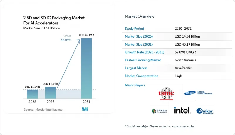
本報告按封裝技術(例如,2.5D IC封裝)、封裝平台(例如,CoWoS、I-Cube、Foveros、EMIB)、應用程式(例如,AI訓練加速器、AI推理加速器)、最終用戶(例如,超大規模資料中心業者和雲端服務供應商、企業AI基礎設施)以及地區進行細分。市場預測以美元(USD)為單位。
面向人工智慧加速器的2.5D和3D IC封裝市場洞察與趨勢
基礎模型訓練運算需求的爆炸性成長
目前,訓練運行次數已超過 1025 次浮點運算,達到 2020 年基準測試的 100 倍。 OpenAI 為 GPT-4 的開發使用了 25,000 個 NVIDIA A100 GPU,而 Llama 3.1 及其 Meta 的 4050 億個參數則消耗了超過 16,000 個 H100S GPU。在這些叢集,HBM3E頻寬在張量核心達到運作之前就已飽和,迫使架構師採用 CoWoS-L 等 2.5D 中介層,以提供 10 TB/s 的晶片間頻寬。雙晶片 GPU 也使供應商能夠更好地利用低良率的晶片單元,從而提高晶圓的整體經濟效益。隨著研究人員的目標是到 2027 年建立 10 兆參數模型,封裝仍將是滿足頻寬和電源需求的主要手段。
雲端資料中心人工智慧加速器的快速更新週期
超大規模資料中心業者正在將加速器更新周期從兩年縮短至一年。微軟將於 2025 年下半年在 Azure 雲端平台部署 Maia 200,Google將於 2025 年開始量產 TPU v8,而 AWS 則於 2024 年推出了 Trainium 2。每個 SKU 都需要將邏輯、記憶體和類比 I/O 晶片整合到單一封裝中。對於延遲敏感型推理應用,垂直堆疊正變得越來越受歡迎,這迫使供應商轉向混合鍵結技術。由於 CoWoS 生產線的前置作業時間為 6-9 個月,因此與代工廠建立長期合作關係對於確保訂單至關重要。
8. 高HBM堆疊以外的收益管理挑戰
SK海力士的12層HBM3E單封裝容量可達36GB,但在回流焊接製程面臨許多挑戰,例如對準公差小於1µm,翹曲度超過50µm,導致良率僅50%左右。三星計劃在2026年採用混合鍵合技術來改進HBM4,但該製程會將表面粗糙度要求提高到亞奈米級,使其對細小顆粒更加敏感。台積電的CoWoS-L製程8層堆疊的良率可達70-80%,但12層堆疊的良率則低於50%,導致每個功能封裝的成本翻倍。在背面供電技術和新型底部填充材料成熟之前,高容量堆疊產品仍將面臨成本挑戰。
細分市場分析
受NVIDIA Blackwell GPU的CoWoS封裝出貨量推動,2.5D IC封裝預計將在2025年佔據88%的營收佔有率。在以AI加速器為導向的2.5D和3D IC封裝市場中,2.5D解決方案市場主要由整合多達八個HBM堆疊和邏輯單元的多光罩矽中介層驅動。然而,由於垂直堆疊可減少90%的訊號路徑,以及能夠從背面供電,3D IC封裝預計將以32.49%的複合年成長率成長。英特爾的Meteor Lake處理器採用PowerVia技術的Foveros Direct封裝,能源效率提升了20%,而三星的X-Cube藍圖也展現了類似的效能。未來五年,邊緣AI推理和低於500W的散熱設計預算將推動設計人員採用能夠最大限度減少尺寸和延遲的3D拓撲結構。
3D封裝技術的應用仍面臨挑戰。它需要在每一層進行「已知良品晶片(KGD)」測試,而晶圓間的對準要求更為嚴格,因此與2.5D中介層鍵結相比,其產能較低。在超過四層主動邏輯層的堆疊結構中,良率仍然會下降,但供應商正在合作最佳化晶片設計、晶圓減薄和熱壓縮工藝,以提高生產線效率。隨著這些挑戰的逐步解決,預計到2031年,3D封裝在人工智慧加速器2.5D和3DIC封裝市場中的佔有率將翻倍。然而,對於需要大橫向面積的記憶體依賴型訓練GPU而言,2.5D中介層仍可能佔據主導地位。
CoWoS憑藉為NVIDIA、AMD和多家超超大規模資料中心業者客製化晶片的業務,預計到2025年將佔據69%的市場佔有率。 CoWoS在人工智慧加速器2.5D和3D IC封裝市場的主導地位,反映了其早期學習曲線優勢以及與台積電4nm和3nm製程節點的前端整合。然而,英特爾的EMIB和Foveros產品線,在Gaudi 3、Ponte Vecchio以及外部代工廠客戶的支持下,正以32.89%的複合年成長率成長。 EMIB透過在有機層壓板中嵌入矽橋,與全面積中介層相比,可將封裝成本降低40%。 Foveros採用10µm間距堆疊晶片,從而降低對毫秒級響應速度要求極高的推理工作負載的延遲。
三星的 I-Cube 及其模組化的 H-Cube、S-Cube 和 X-Cube 衍生產品,使該公司成為以記憶體為中心的設計領域的強大競爭者。來自 OSAT(半導體封裝測試外包服務供應商)的產品,例如 Amkor 的 SWIFT 和 ASE 的 FOCoS,則瞄準了對成本高度敏感的邊緣 AI 市場,在該市場中,封裝厚度和元件成本比絕對頻寬更為重要。未來,平台多樣化將使設計人員能夠結合中介層、橋接器和扇出等技術,選擇滿足工作負載需求的最低成本架構。
區域分析
亞太地區在台灣的CoWoS技術和韓國的HBM生產領域的領先地位的推動下,預計到2025年將佔全球銷售額的65%。台積電計畫在2026年投資520億至560億美元,以達到每月15萬片CoWoS晶圓的產能。同時,三星宣布了2026年高達730億美元的創紀錄資本投資計劃,其中大部分將用於混合鍵結HBM4生產線。此外,日本正向台積電位於熊本的工廠提供63億美元(9,200億日圓)的津貼,以建立其在亞洲的第二個主要生產中心,並降低其對單一地區的依賴。
預計北美將成為成長最快的地區,複合年成長率 (CAGR) 將達到 33.09%。這一成長主要得益於《晶片封裝法案》(CHIPS Act) 下提供的 16 億美元封裝技術津貼金,以及英特爾位於俄亥俄州的製造基地。該基地將前端光刻技術與 Foveros 和 EMIB 等先進的後端技術結合。此外,應用材料公司位於加州桑尼維爾的新研發中心和 Absolix 公司位於喬治亞的玻璃基板製造廠也為該地區關鍵材料供應鏈的最佳化做出了貢獻。
儘管歐洲的市佔率仍相對較低,但總額達430億歐元(470億美元)的《歐洲晶片法案》目前正在支持德國和法國開發中試規模的封裝生產線。相較之下,南美洲和中東/非洲地區發展落後,但正積極尋求與OSAT(外包半導體組裝測試)公司建立合作關係,以支援汽車和工業晶片的生產。巴西Ceitec公司和阿拉伯聯合大公國穆巴達拉投資公司支持的項目等早期舉措已初見成效,但預計到2031年,大規模中介層製造能力仍將集中在亞洲和北美。
其他好處:
- Excel格式的市場預測(ME)表
- 3個月的分析師支持
目錄
第1章:引言
- 研究假設和市場定義
- 調查範圍
第2章:調查方法
第3章執行摘要
第4章 市場狀況
- 市場概覽
- 市場促進因素
- 基礎模型訓練計算需求激增。
- 雲端資料中心人工智慧加速器的快速更新週期
- 主要代工廠的異構整合藍圖
- 政府撥款擴大先進封裝材料的產能
- 推動永續性向低功耗晶片架構轉型
- 垂直整合的人工智慧新創公司尋求客製化的3D軟體包。
- 市場限制因素
- 8. 高HBM堆疊以外的收益管理挑戰
- 供應鏈對小於 10µm 的微凸塊準備不足
- 資本投資的集中給OSAT的盈利帶來了壓力。
- 先進包裝設備的地緣政治出口限制
- 宏觀經濟因素對市場的影響
- 產業價值鏈分析
- 監理情勢
- 技術展望
- 波特五力分析
第5章 市場規模與成長預測
- By Packaging Technology
- 2.5D IC封裝
- 3D IC封裝
- 透過包裝平台
- CoWoS
- I-Cube
- Foveros/EMIB
- 其他客製化先進包裝平台
- 透過使用
- 人工智慧訓練加速器
- AI推理加速器
- 高效能運算加速器
- 最終用戶
- 超大規模資料中心業者雲端服務供應商/雲端服務供應商
- 企業人工智慧基礎設施
- 研究機構和政府附屬人工智慧/高效能運算中心
- 按地區
- 北美洲
- 美國
- 加拿大
- 墨西哥
- 歐洲
- 英國
- 德國
- 法國
- 其他歐洲國家
- 亞太地區
- 中國
- 日本
- 印度
- 韓國
- 其他亞太國家
- 南美洲
- 中東和非洲
- 北美洲
第6章 競爭情勢
- 市場集中度
- 策略趨勢
- 市佔率分析
- 公司簡介
- Taiwan Semiconductor Manufacturing Company Limited
- Samsung Electronics Co. Ltd.
- Intel Corporation
- ASE Technology Holding Co. Ltd.
- Amkor Technology Inc.
- United Microelectronics Corporation
- Powertech Technology Inc.
- Jiangsu Changjiang Electronics Technology Co. Ltd.
- Siliconware Precision Industries Co. Ltd.
- Advanced Micro Devices Inc.
- NVIDIA Corporation
- Broadcom Inc.
- Marvell Technology Inc.
- Xilinx Inc.(AMD)
- Graphcore Ltd.
- Tenstorrent Inc.
- Cerebras Systems Inc.
- Alibaba Group Holding Limited(T-Head)
- Huawei Technologies Co. Ltd.(HiSilicon)
- Google LLC(Tensor Processing Unit)
第7章 市場機會與未來展望
According to Mordor Intelligence, the 2.5D and 3D IC packaging market size is expected to increase from USD 14.84 billion in 2026 to USD 45.19 billion by 2031, growing at a 32.09% CAGR over 2026-2031.
This report is Segmented by Packaging Technology (2. 5D IC Packaging, and More), Packaging Platform (CoWoS, I-Cube, Foveros, and EMIB, and More), Application (AI Training Accelerators, AI Inference Accelerators, and More), End-User (Hyperscalers and Cloud Providers, Enterprise AI Infrastructure, and More), and Geography. The Market Forecasts are Provided in Terms of Value (USD).
Insights and Trends of 2.5D And 3D IC Packaging Market For AI Accelerators
Exploding Training Compute Requirements in Foundation Models
Training runs now exceed 1025 floating-point operations, one hundred times the 2020 benchmark. OpenAI needed 25,000 NVIDIA A100 GPUs for GPT-4, while Meta's 405 billion-parameter Llama 3.1 consumed over 16,000 H100S. These clusters saturate HBM3E bandwidth before tensor cores reach full utilization, forcing architects to adopt 2.5D interposers like CoWoS-L that furnish 10 TB/s die-to-die bandwidth. Dual-die GPUs also let suppliers salvage partially yielding tiles, boosting overall wafer economics. As researchers eye 10-trillion-parameter models by 2027, packaging will remain the prime lever for meeting bandwidth and power-delivery demands.
Rapid AI Accelerator Refresh Cycles in Cloud Data Centers
Hyperscalers are cutting accelerator refresh intervals from two years to one. Microsoft rolled out Maia 200 across Azure in late 2025, Google began TPU v8 volume shipments in 2025, and AWS introduced Trainium 2 in 2024. Each SKU demands packaging that mixes logic, memory, and analog I/O dies in a single footprint. Latency-sensitive inference variants increasingly favor vertical stacking, nudging suppliers toward hybrid bonding. Lead times for CoWoS lines are 6 to 9 months, so long-term foundry alliances become decisive for allocation.
Yield Management Challenges Beyond 8-High HBM Stacks
SK hynix's 12-high HBM3E brings 36 GB per package yet faces alignment tolerances under 1 µm and warpage over 50 µm during reflow, cutting yields to the low-50% range. Samsung plans to counter with hybrid bonding for HBM4 in 2026, but that process tightens surface-roughness specs to sub-nm levels and heightens particulate sensitivity. TSMC's CoWoS-L yields reach 70%-80% at 8-high yet dip below 50% at 12-high, doubling the cost per functional package. Until backside power delivery and new underfill chemistries mature, large-capacity stacks will remain cost-challenged.
Other drivers and restraints analyzed in the detailed report include:
- Heterogeneous Integration Roadmaps of Leading Foundries
- Government Funding for Advanced Packaging Capacity Expansion
- Limited Sub-10 µm Micro-Bump Supply Chain Readiness
For complete list of drivers and restraints, kindly check the Table Of Contents.
Segment Analysis
2.5D IC packaging accounted for 88% of 2025 revenue, aided by CoWoS shipments to NVIDIA Blackwell GPUs. The 2.5D and 3D IC packaging market size for 2.5D solutions is anchored by multi-reticle silicon interposers that integrate logic tiles with up to eight HBM stacks. Still, 3D IC packaging is forecast to grow at a 32.49% CAGR, as vertical stacking collapses signal paths by 90% and unlocks backside power delivery. Intel's Meteor Lake processors show 20% energy gains through PowerVia-enabled Foveros Direct, and Samsung's X-Cube roadmap rivals that performance. Over the next five years, AI inference at the edge and thermal budgets under 500 W will push designers toward 3D topologies that minimize footprint and latency.
Adoption hurdles remain. 3D assembly requires known-good-die testing at each layer and tighter wafer-to-wafer alignment, slowing throughput compared with 2.5D interposer bonding. Yield drag persists for stacks with more than 4 active logic layers, yet suppliers are co-optimizing die design, wafer thinning, and thermal-compression steps to boost line productivity. As these kinks ease, 3D's share of the overall 2.5D and 3D IC packaging market is set to double by 2031, even as 2.5D interposers retain primacy for memory-bound training GPUs that need massive lateral area.
CoWoS secured 69% market share in 2025, fueled by NVIDIA, AMD, and multiple hyperscaler custom chips. The 2.5D and 3D IC packaging market share commanded by CoWoS reflects early learning-curve advantages and front-end integration with TSMC's 4 nm and 3 nm nodes. Yet Intel's EMIB and Foveros lines are logging a 32.89% CAGR, helped by Gaudi 3, Ponte Vecchio, and external foundry customers. EMIB embeds a silicon bridge within an organic laminate, slashing package cost by 40% compared to full-area interposers. Foveros stacks dies at 10 µm pitch, cutting latency for inference workloads that prize millisecond responsiveness.
Samsung's I-Cube introduces modular H-Cube, S-Cube, and X-Cube variants, positioning the Korean firm as a strong alternative in memory-centric designs. OSAT offerings such as Amkor SWIFT and ASE FOCoS target cost-sensitive edge AI markets where package thickness and bill-of-materials costs trump absolute bandwidth. Over time, platform diversity will allow designers to mix interposer, bridge, and fan-out modalities, selecting the lowest-cost architecture that meets workload needs.
Geography Analysis
Asia-Pacific captured 65% of 2025 revenue, driven by Taiwan's dominance in CoWoS technology and South Korea's leadership in HBM production. TSMC is investing between USD 52 billion and USD 56 billion in capital expenditures through 2026, with plans to achieve a production capacity of 150,000 CoWoS wafers per month. Meanwhile, Samsung has announced a record-breaking USD 73 billion capital expenditure plan for 2026, with a significant portion allocated to hybrid-bonded HBM4 production lines. Additionally, Japan has provided a JPY 920 billion (USD 6.3 billion) subsidy for TSMC's Kumamoto site, establishing a second major hub in Asia and reducing reliance on a single geographic location.
North America is projected to be the fastest-growing region, with a compound annual growth rate (CAGR) of 33.09%. This growth is fueled by USD 1.6 billion in CHIPS Act packaging grants and Intel's Ohio fabrication complex, which integrates front-end lithography with advanced back-end technologies such as Foveros and EMIB. Furthermore, Applied Materials' new research center in Sunnyvale, California, and Absolics' glass-substrate manufacturing facility in Georgia are helping to streamline critical-materials supply chains within the region.
Europe's market share remains relatively modest; however, the EUR 43 billion (USD 47 billion) European Chips Act is now supporting the development of pilot packaging lines in Germany and France. In contrast, South America, the Middle East, and Africa are lagging but are actively pursuing OSAT partnerships to support the production of automotive and industrial chips. Early initiatives, such as Brazil's Ceitec and the UAE's Mubadala-backed ventures, are making progress, though large-scale interposer manufacturing capacity is expected to remain concentrated in Asia and North America through 2031.
- Taiwan Semiconductor Manufacturing Company Limited
- Samsung Electronics Co. Ltd.
- Intel Corporation
- ASE Technology Holding Co. Ltd.
- Amkor Technology Inc.
- United Microelectronics Corporation
- Powertech Technology Inc.
- Jiangsu Changjiang Electronics Technology Co. Ltd.
- Siliconware Precision Industries Co. Ltd.
- Advanced Micro Devices Inc.
- NVIDIA Corporation
- Broadcom Inc.
- Marvell Technology Inc.
- Xilinx Inc. (AMD)
- Graphcore Ltd.
- Tenstorrent Inc.
- Cerebras Systems Inc.
- Alibaba Group Holding Limited (T-Head)
- Huawei Technologies Co. Ltd. (HiSilicon)
- Google LLC (Tensor Processing Unit)
Additional Benefits:
- The market estimate (ME) sheet in Excel format
- 3 months of analyst support
TABLE OF CONTENTS
1 INTRODUCTION
- 1.1 Study Assumptions and Market Definition
- 1.2 Scope of the Study
2 RESEARCH METHODOLOGY
3 EXECUTIVE SUMMARY
4 MARKET LANDSCAPE
- 4.1 Market Overview
- 4.2 Market Drivers
- 4.2.1 Exploding Training Compute Requirements in Foundation Models
- 4.2.2 Rapid AI Accelerator Refresh Cycles in Cloud Data Centers
- 4.2.3 Heterogeneous Integration Roadmaps of Leading Foundries
- 4.2.4 Government Funding for Advanced Packaging Capacity Expansion
- 4.2.5 Sustainability Push Toward Lower-Power Chiplet Architectures
- 4.2.6 Vertical AI Start-Ups Demanding Custom 3D Packages
- 4.3 Market Restraints
- 4.3.1 Yield Management Challenges Beyond 8-High HBM Stacks
- 4.3.2 Limited Sub-10 µm Micro-Bump Supply Chain Readiness
- 4.3.3 CapEx Intensity Straining OSAT Profitability
- 4.3.4 Geopolitical Export Controls on Advanced Packaging Tools
- 4.4 Impact of Macroeconomic Factors on the Market
- 4.5 Industry Value Chain Analysis
- 4.6 Regulatory Landscape
- 4.7 Technological Outlook
- 4.8 Porter's Five Forces Analysis
- 4.8.1 Bargaining Power of Suppliers
- 4.8.2 Bargaining Power of Buyers
- 4.8.3 Threat of New Entrants
- 4.8.4 Threat of Substitutes
- 4.8.5 Intensity of Competitive Rivalry
5 MARKET SIZE AND GROWTH FORECASTS (VALUE)
- 5.1 By Packaging Technology
- 5.1.1 2.5D IC Packaging
- 5.1.2 3D IC Packaging
- 5.2 By Packaging Platform
- 5.2.1 CoWoS
- 5.2.2 I-Cube
- 5.2.3 Foveros / EMIB
- 5.2.4 Other Custom Advanced Packaging Platforms
- 5.3 By Application
- 5.3.1 AI Training Accelerators
- 5.3.2 AI Inference Accelerators
- 5.3.3 HPC Accelerators
- 5.4 By End-User
- 5.4.1 Hyperscalers / Cloud Providers
- 5.4.2 Enterprise AI Infrastructure
- 5.4.3 Research and Government AI/HPC Centers
- 5.5 By Geography
- 5.5.1 North America
- 5.5.1.1 United States
- 5.5.1.2 Canada
- 5.5.1.3 Mexico
- 5.5.2 Europe
- 5.5.2.1 United Kingdom
- 5.5.2.2 Germany
- 5.5.2.3 France
- 5.5.2.4 Rest of Europe
- 5.5.3 Asia-Pacific
- 5.5.3.1 China
- 5.5.3.2 Japan
- 5.5.3.3 India
- 5.5.3.4 South Korea
- 5.5.3.5 Rest of Asia-Pacific
- 5.5.4 South America
- 5.5.5 Middle East and Africa
- 5.5.1 North America
6 COMPETITIVE LANDSCAPE
- 6.1 Market Concentration
- 6.2 Strategic Moves
- 6.3 Market Share Analysis
- 6.4 Company Profiles (includes Global Level Overview, Market Level Overview, Core Segments, Financials as available, Strategic Information, Market Rank/Share, Products and Services, Recent Developments)
- 6.4.1 Taiwan Semiconductor Manufacturing Company Limited
- 6.4.2 Samsung Electronics Co. Ltd.
- 6.4.3 Intel Corporation
- 6.4.4 ASE Technology Holding Co. Ltd.
- 6.4.5 Amkor Technology Inc.
- 6.4.6 United Microelectronics Corporation
- 6.4.7 Powertech Technology Inc.
- 6.4.8 Jiangsu Changjiang Electronics Technology Co. Ltd.
- 6.4.9 Siliconware Precision Industries Co. Ltd.
- 6.4.10 Advanced Micro Devices Inc.
- 6.4.11 NVIDIA Corporation
- 6.4.12 Broadcom Inc.
- 6.4.13 Marvell Technology Inc.
- 6.4.14 Xilinx Inc. (AMD)
- 6.4.15 Graphcore Ltd.
- 6.4.16 Tenstorrent Inc.
- 6.4.17 Cerebras Systems Inc.
- 6.4.18 Alibaba Group Holding Limited (T-Head)
- 6.4.19 Huawei Technologies Co. Ltd. (HiSilicon)
- 6.4.20 Google LLC (Tensor Processing Unit)
7 MARKET OPPORTUNITIES AND FUTURE OUTLOOK
- 7.1 White-Space and Unmet-Need Assessment

 先進積IC封裝市場-2026年至2032年全球市場預測
 2.5D 和 3D IC封裝市場預測至 2034 年—全球封裝技術、互連技術、材料、應用、最終用戶和區域分析3D IC 和 2.5D IC封裝市場:按封裝技術、組件、基礎設施和應用分類-2026-2032 年全球市場預測電源管理IC封裝市場:2026-2032年全球市場預測(依元件類型、封裝類型、封裝材料、佈線技術、應用與最終用途產業分類)
 3D IC 和 2.5D IC封裝市場規模、佔有率和成長分析:按封裝技術、應用、終端用戶產業和地區分類-2026-2033 年產業預測IC封裝市場預測至2034年-全球分析(整體封裝類型、互連技術、材料類型、晶圓尺寸、最終用途元件、服務類型、應用、經營模式和地區分類)軟性電子材料市場預測至2034年-按材料類型、組件、技術、應用和地區分類的全球分析
 3D IC 和 2.5D IC封裝市場:按封裝技術、整合技術、封裝平台、應用、終端設備和材料分類-市場規模、產業動態、機會分析和預測(2026-2035 年)
 3D IC 和 2.5D IC封裝市場分析及預測(至 2035 年):按類型、產品、服務、技術、組件、應用、材料類型、製程、最終用戶和設備分類
 2026年全球攜帶式無線保真度(Wi-Fi)市場報告