

 |
市場調查報告書
商品編碼
2063403
類比IC體電路用矽晶圓:市場佔有率分析、產業趨勢與統計數據以及成長預測(2026-2031 年)Silicon Wafer For Analog ICs - Market Share Analysis, Industry Trends & Statistics, Growth Forecasts (2026 - 2031) |
||||||
※ 本網頁內容可能與最新版本有所差異。詳細情況請與我們聯繫。
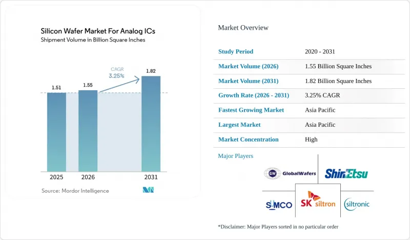
根據 Mordor Intelligence 的數據,類比IC矽晶圓市場(以出以出貨量為準)預計到 2025 年將達到 15.1 億平方英寸,到 2026 年將達到 15.5 億平方英寸,到 2031 年將達到 18.2 億平方英寸,2026 年至 203% 3.325% 3.3% 203%。
本報告按晶圓直徑(150毫米及以下、200毫米、300毫米)、晶圓類型(拋光晶圓、外延晶圓、SOI晶圓、特種矽晶圓)、最終用戶(消費性電子、工業、汽車及其他)和地區(北美、歐洲、亞太、南美、中東和非洲)進行細分。市場預測以出貨量(平方英吋)為基礎。
類比IC矽晶圓市場的趨勢與發展
擴大300mm晶圓廠低功耗類比IC的生產能力。
晶圓代工廠正斥資數十億美元建造300毫米生產線,目標是實現28奈米以上的類比晶片製程。這是因為即使良率不如最先進的邏輯晶片,更大的晶圓尺寸也能降低晶圓成本。 GlobalWafers在德克薩斯州投資75億美元的項目以及Siltronic在德國和新加坡投資20億歐元的項目,都清楚地展現了這一轉變的規模。德州儀器正在Richardson和Lehigh複製這個模式,並利用CHIPS的津貼來抵消資本密整合本。 SEMI預測,2026年至2028年間,類比、功率和分立元件晶圓廠的設備投資將超過410億美元。這些投資將推動類比IC的矽晶圓市場在2020年代末期轉向300毫米生產。
電動車快速充電對高壓電源管理積體電路(PMIC)的需求不斷成長
工作電壓超過 800V 的快速充電系統需要缺陷密度低於 0.05 cm⁻² 的外延矽晶片,以防止災難性故障。瑞薩電子、亞德諾半導體和恩智浦半導體均提供符合 ISO 26262 安全標準的 42V-60V 額定電壓的電源管理積體電路 (PMIC)。國際能源總署 (IEA) 預測,到 2025 年,電動車銷量將超過 1,700 萬輛,預計這將推動基板的需求成長。因此,能夠保證嚴格電阻率控制的特殊矽供應商正在與汽車整合裝置製造商 (IDM) 簽訂長期供貨協議。
對模擬IDM進行定期資本投資
汽車和工業客戶正在迅速調整訂單,迫使類比積體電路製造商 (IDM) 限制晶圓廠的運轉率。信越化學在 2025 年 10 月進行汽車庫存調整後報告稱,200 毫米晶圓的需求有所疲軟。德州儀器在 2024 年提交的文件中宣布推遲生產設備的部署。這些週期性延遲正在對晶圓的平均售價 (ASP) 構成下行壓力,並顯著增加與供應商營運資金相關的風險。
細分市場分析
2025年,200mm級晶片佔據了類比IC電路矽晶圓市場74.74%的佔有率。然而,隨著德州儀器和全球晶圓製造商推進更大尺寸基板上低功耗類比電路的認證,預計到2031年,300mm級晶片的複合年成長率將達到3.89%。透過在晶圓廠改造中利用通用的光刻工藝,模擬積體電路元件無需節點小型化即可降低30-40%的晶圓成本。早期採用者正專注於具有靈活且容錯性高的佈局設計規則的電源管理整合電路(PMIC)和數據轉換器系列,以確保300mm設備投資的快速回報。
儘管150mm以下晶圓仍存在一定的市場需求,主要用於高壓閘流體和研發試點應用,但隨著設備製造商將生產線擴展至200mm翻新生產線,預計該市場將持續萎縮。同時,200mm晶圓的產能依然緊張。由於汽車產業的庫存波動,短期需求已疲軟,但工業機器人和可再生能源領域的需求仍在持續吸收成熟節點的供應。在預測期內,300mm晶圓供應量的增加預計將重新平衡直徑分佈,類比IC矽晶圓市場的成本結構也將更加多元化。
區域分析
預計到2025年,亞太地區將佔全球矽晶圓出貨量的67.77%,佔據類比IC矽晶圓市場最大佔有率,並以4.06%的複合年成長率在2031年繼續保持領先地位。台積電(TSMC)、新光電子(Simgui)和SK Siltron等公司提升的產能主要集中在300mm晶圓生產線,以支援高壓電源管理積體電路(PMIC)和毫米波射頻晶片的生產。儘管全球經濟週期放緩,但中國大力推動國內採購,維持了強勁的需求;同時,日本的Rapidus專案也推動了混合訊號節點的平行發展。韓國的優勢在於地理位置靠近汽車電子產品出口國,這些出口國需要成熟節點的可靠性。該地區晶圓廠和材料供應商的密集分佈縮短了物流週期,並增強了其成本優勢。
預計到2025年,北美將佔據15%左右的市場佔有率,並且其成長速度超過全球平均水平,這得益於《晶片和整合產品法案》(CHIPS Act)的獎勵降低了新建模擬晶片產能的風險。 GlobalWafers、德州儀器和安森美半導體正在建造或擴建300毫米晶圓廠,目標是在2020年代末期實現每月超過100萬片晶圓的總合產量。汽車、國防和資料中心客戶傾向於選擇國內採購,以規避地緣政治風險並縮短認證流程。這些趨勢正在提高現有200毫米生產線的運轉率,同時也為新建待開發區專案提供了資金籌措支援。
歐洲的市佔率維持在兩位數的低位,這主要得益於英飛凌、義法半導體以及歐盟晶片法案提供的補貼,該法案旨在促進全球晶圓代工廠的擴張。德國德勒斯登工廠正在崛起為汽車混合訊號晶片的生產中心,而義大利卡塔尼亞工廠則專注於碳化矽外延技術。英國和法國在射頻SOI和感測器級晶圓等特殊產品的生產方面做出了貢獻,但在大規模供應大型拋光晶圓方面則依賴進口。南美、中東和非洲的總合佔有率合計仍不足5%,但可再生的細分市場需求,這可能會在未來十年後半期吸引當地的拋光和切割企業。
其他好處
- Excel格式的市場預測(ME)表
- 3個月的分析師支持
目錄
第1章:引言
- 研究假設和市場定義
- 調查範圍
第2章:調查方法
第3章執行摘要
第4章 市場狀況
- 市場概覽
- 市場促進因素
- 擴大300mm晶圓廠低功耗類比IC的生產能力。
- 電動車快速充電對高壓電源管理積體電路(PMIC)的需求不斷成長
- 5G大規模MIMO無線電中模擬前端的整合
- 向寬能隙閘極驅動器過渡需要超低缺陷晶圓
- 《CHIPS法案》和《歐盟CHIPS法案》規定的遣返獎勵
- 透過引入人工智慧驅動的製程控制來降低缺陷率。
- 市場限制因素
- 基於週期的模擬IDM資本投資
- 高純度多晶矽原料供應緊張
- 毫米波射頻應用中 200mm 或更大尺寸 SOI 晶圓的良率挑戰。
- 水和能源利用永續性的壓力
- 產業價值鏈分析
- 監理情勢
- 技術分析
- 宏觀經濟因素的影響
- 波特五力分析
第5章 市場規模及成長預測(按地區分類的出貨量)
- 依晶圓直徑
- 150毫米或更小
- 200mm
- 300mm
- 依晶片類型
- 拋光劑
- 外延
- 絕緣體上矽(SOI)
- 特種矽(高電阻、高功率、感測器級)
- 最終用戶
- 家用電器
- 行動裝置和智慧型手機
- PC 和伺服器
- 工業的
- 用於溝通
- 汽車
- 其他終端用戶應用程式
- 家用電器
- 按地區
- 北美洲
- 美國
- 加拿大
- 墨西哥
- 歐洲
- 德國
- 英國
- 法國
- 其他歐洲國家
- 亞太地區
- 中國
- 日本
- 印度
- 韓國
- 台灣
- 其他亞太國家
- 南美洲
- 中東
- 非洲
- 北美洲
第6章 競爭情勢
- 市場集中度
- 策略趨勢
- 市佔率分析
- 公司簡介
- Shin-Etsu Chemical Co., Ltd.
- SUMCO Corporation
- GlobalWafers Co., Ltd.
- Siltronic AG
- SK Siltron Co., Ltd.
- Wafer Works Corporation
- Soitec SA
- Siltronix Silicon Technologies
- MEMC Electronic Materials Inc.
- Shanghai Simgui Technology Co., Ltd.
- Topsil Semiconductor Materials A/S
- Okmetic Oyj
- Addison Engineering, Inc.
- Grinm Semiconductor Materials Co., Ltd.
- GT Advanced Technologies Inc.
- Wafer World Inc.
- Coherent Corp.(II-VI)
- Nova Electronic Materials
- Elkem ASA
- Mitsui Mining & Smelting Co., Ltd.
第7章 市場機會與未來展望
According to Mordor Intelligence, the silicon wafer market for analog ICs industry size in terms of shipment volume is projected to be 1.51 Billion Square Inches in 2025, 1.55 Billion Square Inches in 2026, and reach 1.82 Billion Square Inches by 2031, growing at a CAGR of 3.25% from 2026 to 2031.
This report is Segmented by Wafer Diameter (Up To 150 Mm, 200 Mm, 300 Mm), Wafer Type (Prime Polished, Epitaxial, Silicon-On-Insulator, Specialty Silicon), End-User (Consumer Electronics, Industrial, Automotive, and More), and Geography (North America, Europe, Asia-Pacific, South America, Middle East, Africa). The Market Forecasts are Provided in Terms of Shipment Volume (Square Inches).
Insights and Trends of Silicon Wafer Market For Analog ICs
Capacity Expansion by 300 mm Foundries for Power-Efficient Analog ICs
Foundries are channeling multi-billion-dollar outlays into 300 mm lines targeting analog nodes above 28 nm, because larger wafers trim die costs even when yields lag those of leading-edge logic. GlobalWafers' USD 7.5 billion Texas project and Siltronic's EUR 2 billion German-Singapore plan illustrate the scale of this pivot. Texas Instruments is replicating the model in Richardson and Lehi, using CHIPS grants to offset the capital intensity. SEMI forecasts that analog, power, and discrete fabs will absorb more than USD 41 billion in equipment from 2026-2028. These investments position the silicon wafer market for analog ICs to shift its center of gravity toward 300 mm production by the end of the decade.
Growing Demand for High-Voltage PMICs in EV Fast-Charging
Fast-charging systems operating above 800 V require epitaxial silicon wafers with defect densities below 0.05 cm-2 to prevent catastrophic breakdown. Renesas, Analog Devices, and NXP have all introduced PMICs rated 42 V-60 V that meet ISO 26262 safety levels. The International Energy Agency expects EV sales to exceed 17 million units in 2025, amplifying substrate demand tied to 350 kW chargers. Specialty silicon suppliers that can guarantee tight control of resistivity are therefore securing long-term supply contracts with automotive IDMs.
Cyclical Capital Expenditure of Analog IDMs
Automotive and industrial customers adjust orders quickly, forcing analog IDMs to throttle fab utilization. Shin-Etsu Chemical reported softer 200 mm volumes after automotive inventory corrections in October 2025. In its 2024 filings, Texas Instruments announced the postponement of its tool installations. These cyclical delays exert downward pressure on wafer Average Selling Prices (ASPs) and significantly increase the risks associated with working capital for suppliers.
Other drivers and restraints analyzed in the detailed report include:
- Analog Front-End Integration in 5G Massive-MIMO Radios
- Transition to Wide-Bandgap Gate Drivers Requiring Ultra-Low Defect Wafers
- Supply Tightness of High-Purity Polysilicon Feedstock
For complete list of drivers and restraints, kindly check the Table Of Contents.
Segment Analysis
The 200 mm class captured 74.74% of the analog ICs silicon wafer market share in 2025. However, the 300 mm category is on track for a 3.89% CAGR to 2031 as Texas Instruments and GlobalWafers qualify power-efficient analog flows on larger substrates. Fab conversions exploit common lithography footprints, allowing analog IDMs to slice 30%-40% from die cost without node shrinks. Early adopters focus on PMICs and data-converter families whose layouts tolerate relaxed design rules, ensuring quick returns on 300 mm capex.
A residual niche of up to 150 mm persists for high-voltage thyristors and R&D pilots, but will continue to contract as equipment makers extend their toolsets to 200 mm refurb lines. Meanwhile, 200 mm capacity remains constrained; inventory swings in automotive cause short-term softness, yet industrial robot and renewable-energy demand continue to absorb mature-node supply. Over the forecast, rising 300 mm availability will rebalance the diameter mix, nudging the silicon wafer market for analog ICs toward a more diversified cost base.
Geography Analysis
Asia-Pacific commanded 67.77% of 2025 shipments, giving the region the largest share of the analog ICs silicon wafer market and a leading 4.06% CAGR through 2031. Capacity additions by Taiwan Semiconductor Manufacturing Company, Simgui, and SK Siltron are concentrated on 300 mm lines that support high-voltage PMICs and millimeter-wave RF chips. China's drive for domestic sourcing keeps demand resilient even when global cycles soften, while Japan's Rapidus project anchors a parallel push into mixed-signal nodes. Korea benefits from proximity to automotive electronics exporters that require mature-node reliability. The region's tight cluster of fabs and materials vendors shortens logistics cycles and reinforces its cost advantage.
North America held a mid-teens share in 2025 and is growing faster than the global average as CHIPS Act incentives de-risk new analog capacity. GlobalWafers, Texas Instruments, and Onsemi are building or expanding 300 mm plants that collectively aim to reach more than 1 million wafers per month by the late 2020s. Automotive, defense, and datacenter customers prefer domestic sourcing to hedge geopolitical risk and shorten qualification loops. These trends improve utilization of existing 200 mm lines while underpinning financing for new greenfield sites.
Europe maintained a low-double-digit share, helped by EU Chips Act subsidies supporting Infineon, STMicroelectronics, and GlobalFoundries' expansions. Germany's Dresden hub is emerging as a center for automotive-grade mixed-signal production, while Italy's Catania facility focuses on silicon-carbide epitaxy. The United Kingdom and France contribute specialty output for RF-SOI and sensor-grade wafers, yet rely on imports for prime polished volume. South America, the Middle East, and Africa together remain below a 5% share, though renewable-energy and telecom projects are creating niche demand that may invite local polishing or slicing operations later in the decade.
- Shin-Etsu Chemical Co., Ltd.
- SUMCO Corporation
- GlobalWafers Co., Ltd.
- Siltronic AG
- SK Siltron Co., Ltd.
- Wafer Works Corporation
- Soitec S.A.
- Siltronix Silicon Technologies
- MEMC Electronic Materials Inc.
- Shanghai Simgui Technology Co., Ltd.
- Topsil Semiconductor Materials A/S
- Okmetic Oyj
- Addison Engineering, Inc.
- Grinm Semiconductor Materials Co., Ltd.
- GT Advanced Technologies Inc.
- Wafer World Inc.
- Coherent Corp. (II-VI)
- Nova Electronic Materials
- Elkem ASA
- Mitsui Mining & Smelting Co., Ltd.
Additional Benefits:
- The market estimate (ME) sheet in Excel format
- 3 months of analyst support
TABLE OF CONTENTS
1 INTRODUCTION
- 1.1 Study Assumptions and Market Definition
- 1.2 Scope of the Study
2 RESEARCH METHODOLOGY
3 EXECUTIVE SUMMARY
4 MARKET LANDSCAPE
- 4.1 Market Overview
- 4.2 Market Drivers
- 4.2.1 Capacity Expansion by 300 mm Foundries for Power-Efficient Analog ICs
- 4.2.2 Growing Demand for High-Voltage PMICs in EV Fast-Charging
- 4.2.3 Analog Front-End Integration in 5G Massive-MIMO Radios
- 4.2.4 Transition to Wide-Bandgap Gate Drivers Requiring Ultra-Low Defect Wafers
- 4.2.5 On-shoring Incentives under CHIPS and EU Chips Acts
- 4.2.6 Adoption of AI-Based Process Control Reducing Scrap Rates
- 4.3 Market Restraints
- 4.3.1 Cyclical Capital Expenditure of Analog IDMs
- 4.3.2 Supply Tightness of High-Purity Polysilicon Feedstock
- 4.3.3 Yield Challenges in >=200 mm SOI Wafers for mmWave RF
- 4.3.4 Sustainability Pressures on Water and Energy Usage
- 4.4 Industry Value-Chain Analysis
- 4.5 Regulatory Landscape
- 4.6 Technology Analysis
- 4.7 Impact of Macroeconomic Factors
- 4.8 Porter's Five Forces Analysis
- 4.8.1 Bargaining Power of Suppliers
- 4.8.2 Bargaining Power of Buyers
- 4.8.3 Threat of New Entrants
- 4.8.4 Threat of Substitutes
- 4.8.5 Intensity of Competitive Rivalry
5 MARKET SIZE AND GROWTH FORECASTS (SHIPMENT IN AREA)
- 5.1 By Wafer Diameter
- 5.1.1 Up to 150 mm
- 5.1.2 200 mm
- 5.1.3 300 mm
- 5.2 By Wafer Type
- 5.2.1 Prime Polished
- 5.2.2 Epitaxial
- 5.2.3 Silicon-on-Insulator (SOI)
- 5.2.4 Specialty Silicon (High-Resistivity, Power, Sensor-Grade)
- 5.3 By End-user
- 5.3.1 Consumer Electronics
- 5.3.1.1 Mobile and Smartphones
- 5.3.1.2 PCs and Servers
- 5.3.2 Industrial
- 5.3.3 Telecommunications
- 5.3.4 Automotive
- 5.3.5 Other End-user Applications
- 5.3.1 Consumer Electronics
- 5.4 By Geography
- 5.4.1 North America
- 5.4.1.1 United States
- 5.4.1.2 Canada
- 5.4.1.3 Mexico
- 5.4.2 Europe
- 5.4.2.1 Germany
- 5.4.2.2 United Kingdom
- 5.4.2.3 France
- 5.4.2.4 Rest of Europe
- 5.4.3 Asia-Pacific
- 5.4.3.1 China
- 5.4.3.2 Japan
- 5.4.3.3 India
- 5.4.3.4 South Korea
- 5.4.3.5 Taiwan
- 5.4.3.6 Rest of Asia-Pacific
- 5.4.4 South America
- 5.4.5 Middle East
- 5.4.6 Africa
- 5.4.1 North America
6 COMPETITIVE LANDSCAPE
- 6.1 Market Concentration
- 6.2 Strategic Moves
- 6.3 Market Share Analysis
- 6.4 Company Profiles (includes Global Level Overview, Market Level Overview, Core Segments, Financials as available, Strategic Information, Market Rank/Share, Products and Services, Recent Developments)
- 6.4.1 Shin-Etsu Chemical Co., Ltd.
- 6.4.2 SUMCO Corporation
- 6.4.3 GlobalWafers Co., Ltd.
- 6.4.4 Siltronic AG
- 6.4.5 SK Siltron Co., Ltd.
- 6.4.6 Wafer Works Corporation
- 6.4.7 Soitec S.A.
- 6.4.8 Siltronix Silicon Technologies
- 6.4.9 MEMC Electronic Materials Inc.
- 6.4.10 Shanghai Simgui Technology Co., Ltd.
- 6.4.11 Topsil Semiconductor Materials A/S
- 6.4.12 Okmetic Oyj
- 6.4.13 Addison Engineering, Inc.
- 6.4.14 Grinm Semiconductor Materials Co., Ltd.
- 6.4.15 GT Advanced Technologies Inc.
- 6.4.16 Wafer World Inc.
- 6.4.17 Coherent Corp. (II-VI)
- 6.4.18 Nova Electronic Materials
- 6.4.19 Elkem ASA
- 6.4.20 Mitsui Mining & Smelting Co., Ltd.
7 MARKET OPPORTUNITIES AND FUTURE OUTLOOK
- 7.1 White-Space and Unmet-Need Assessment
 類比IC市場預測至2034年-全球分析(依產品類型、技術、訊號類型、晶圓尺寸、應用、最終用戶、通路及地區分類)
 2026年全球金屬氧化物半導體(MOS)通用邏輯市場報告2026年全球消費積體電路市場報告
 應用特定標準產品(ASSP)市場:按類型、應用和地區分類 2026-2034 年電壓監測IC市場:按類型、應用和地區分類(2026-2034年)
 類比IC市場:按產品類型、應用和地區分類
 奈米功率比較器市場報告:趨勢、預測和競爭分析(至2035年)
 通用逆變器-2026 年至 2032 年全球市佔率和排名,以及總銷售額和需求預測。
 類比IC市場:全球市場按產品類型、技術、最終用戶和銷售管道分類的預測 - 2026-2032 年2026年全球半導體時序積體電路(IC)市場報告