


 |
市場調查報告書
商品編碼
2062126
銦:市場佔有率分析、產業趨勢與統計、成長預測(2026-2031)Indium - Market Share Analysis, Industry Trends & Statistics, Growth Forecasts (2026 - 2031) |
||||||
※ 本網頁內容可能與最新版本有所差異。詳細情況請與我們聯繫。
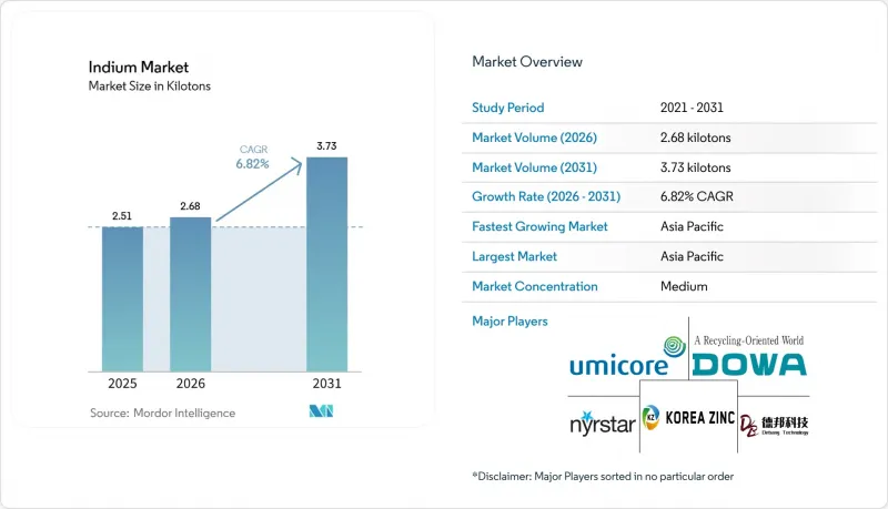
根據 Mordor Intelligence 預測,銦市場規模將在 2025 年達到 2.51 千噸,2026 年達到 2.68 千噸,2031 年達到 3.73 千噸,2026 年至 2031 年的複合年成長率為 6.82%。
本報告按原料(初級原料(鋅渣精煉)和次級原料/回收材料)、形態(例如,高純度銦化合物)、應用(例如,平板顯示器和軟性顯示器)、終端用戶產業(例如,電子和半導體產業)以及地區(亞太地區、北美地區、歐洲地區、南美地區以及中東和非洲地區)進行細分。市場預測以噸為單位。
全球銦市場趨勢及洞察
擴大ITO在下一代軟性折疊式顯示器中的應用
在軟性OLED(有機發光二極體)和折疊式智慧型手機面板中,氧化銦錫(ITO)因其無與倫比的透明度和導電性而備受青睞。低溫濺鍍和後退火製程使得即使在彎曲半徑小於5毫米的情況下,表面電阻率也能保持在15 Ω/sq以下。隨著多層堆疊技術的普及,每塊面板的銦用量也不斷增加。三星顯示器和京東方電子(BOE)計畫分別於2025年開始量產其第六代AMOLED(主動矩陣有機發光二極體)生產線,與傳統的剛性顯示器相比,這將消耗約20-30%的ITO靶材。在高階平板電腦和汽車資訊顯示器中採用ITZO(氧化銦錫鋅)和ITO-銀網結構,進一步增加了5-8%的銦用量,以抑制低溫製程條件下的結晶。預計 2025 年至 2028 年間,折疊式設備的出貨量將增加三倍,如果維持目前的運轉率,這將使銦的年需求量增加 80 至 100 噸。
低溫銦合金在先進封裝和異質整合的應用拓展
在覆晶球柵陣列和大型人工智慧加速器封裝中,採用的銦和銦銀導熱界面材料可實現 71–86 W/m*K 的導熱係數,並能承受 1000 次熱循環。 SAC-In 焊料可將回流焊接溫度降低 15–20 度C,並減少複雜晶片組件的翹曲。晶圓代工廠預測,到 2028 年,在 2.5D 和 3D 堆疊技術的普及推動下,銦基微凸塊鍵結的年需求量將達到 40–50 噸。英特爾和台積電的藍圖都強調低溫鍵結是提高良率的關鍵,間接支持了上述消費預測。
可替代的透明導電材料(石墨烯、銀奈米線、碳奈米管、氧化銦鎵鋅)
美國對中國銦化合物徵收的關稅將於2025年生效,這將加速石墨烯和銀奈米線(Ag-NW)薄膜在北美和歐洲的普及應用。目前,Cambrios和C3Nano的產品在軟式電路板上實現了低於10 Ω/sq的電阻值,同時保持了90%以上的透光率。雷射退火氧化石墨烯具有優異的機械柔順性,但其成本仍比濺鍍ITO高出3到5倍。 IGZO(氧化銦鎵鋅)背板無需單獨的透明導電層,可將每塊面板的銦用量減少高達20%。由於顯示器製造廠依賴成熟的ITO製程,預計到2031年,這些替代方案的市佔率將穩定在15%左右。
細分市場分析
截至2025年,原生銦產量佔銦市場規模的67.78%,但鋅礦品位趨於穩定以及中國新出口許可證的影響抑制了其成長。韓國鋅業投資74億美元的田納西州綜合體項目將是近20年來西半球首個大規模擴建項目,但預計要到2029年或更晚才能運作。再生銦供應正在加速成長,中國年增268%,全球回收率接近15%。銦業株式會社、DOWA公司和三井礦業冶煉公司目前承諾廢棄濺鍍靶材的回收率達到90%,顯示循環經濟帶來的溢價正逐漸成為主流。
預計在預測期(2026-2031年)內,再生/回收原料的供應量將以7.22%的複合年成長率成長,是原生原料成長速度的兩倍。到2031年,回收效率可望達到50-60%。歐盟和加州根據《巴塞爾公約》和生產者延伸責任制對電子廢棄物實施出口限制,促使更多廢棄物流向獲得許可的精煉廠。如果斯維爾多普模型預測的200-300噸的潛在回收量得以實現,回收量將滿足預計需求的約五分之一,從而緩解銦市場規模的壓力,同時減少生命週期排放。
預計到2025年,高純度銦化合物將佔銦市場佔有率的45.22%,並在2031年之前以7.03%的複合年成長率成長,這主要得益於對InP雷射、InGaAs檢測器和InSb紅外線陣列的強勁需求。 Lumentum位於綠波市、佔地24萬平方英尺的工廠預計於2028年開始量產6吋InP晶圓,為6N至7N級原料帶來穩定的需求。 IMEC的「智慧切割」晶圓回收平台預計將基板損耗降低十倍,並減少金屬的長期使用。
錠材、棒材和合金市場的價格走勢仍與鋅的經濟趨勢密切相關,與倫敦金屬交易所(LME)的鋅價基本一致,但複合鋅的價格反映了半導體潔淨室應用領域30%至50%的純度溢價。導熱係數高達86 W/m*K的銦銀合金正在人工智慧加速器的溫度控管領域佔據越來越大的市場佔有率。這種兩極化的價格趨勢凸顯了專用光電元件如何使銦市場免受純金屬價格週期性波動的影響。
區域分析
預計到2025年,亞太地區將佔全球銦市場規模的48.66%,並將在2031年之前保持所有地區中最快的成長速度,複合年成長率(CAGR)為7.43%。儘管中國佔據了精煉銦產量的大部分,但韓國鋅業的國內冶煉以及雲南錫業在氧化銦錫(ITO)靶材方面的技術進步,正在鞏固主導地位。日本的DOWA和三井礦業冶煉公司則專注於高純度和再生銦產品,這使得它們受鋅價波動的影響較小。
北美正從純粹的進口地區轉型為部分生產地區。韓國鋅業位於克拉克斯維爾的工廠將於2029年投產,該工廠與Lumentum公司的InP雷射製造廠將攜手合作,共同打造穩定的區域供應鏈。中國對銦化合物徵收的301條款關稅(實際稅率約為54%)進一步促進了國內採購。
歐洲的「基本原料法」規定,歐洲地區必須滿足10%的採礦量和40%的加工量要求,促使義大利撥款4.5億歐元(約5.087億美元)用於建立200噸的國家儲備。 Imec公司的NanoIC試點生產線於2026年2月運作,將進一步提升下游對7N銦化合物的需求。儘管南美洲和中東及非洲地區的總合佔有率仍低於10%,但如果鋅價持續高於每公斤500美元,巴西和南非的閒置鋅礦資產或可轉化為可調配的產能。
其他好處:
- Excel格式的市場預測(ME)表
- 3個月的分析師支持
目錄
第1章:引言
- 研究假設和市場定義
- 調查範圍
第2章:調查方法
第3章執行摘要
第4章 市場狀況
- 市場概覽
- 市場促進因素
- 擴大ITO在下一代軟性折疊式顯示器中的應用
- 低溫銦合金在先進封裝和異質整合的廣泛應用。
- 關鍵原料的韌性政策正在擴大歐洲的戰略儲備。
- 全球高效能太陽能板生產擴張
- 用於 AR/ VR頭戴裝置的InGaN 微型 LED 的需求正在激增。
- 市場限制因素
- 可替代的透明導電材料(石墨烯、銀奈米線、碳奈米管、氧化銦鎵鋅)
- 長期存在的職業健康問題促使人們制定更嚴格的暴露限值。
- ESG主導的脫碳給銦回收冶煉廠帶來了壓力
- 價值鏈分析
- 波特五力模型
第5章 市場規模與成長預測
- 按原料
- 初級(去除鋅殘渣)
- 二次原料/回收原料
- 按形式
- 銦錠和銦棒
- 銦合金(In-Sn、In-Ag、In-Ga)
- 氧化銦/ITO濺鍍靶材
- 高純度銦化合物(InP、InSb、InAs)
- 透過使用
- 平面和軟性顯示器
- 太陽能發電(CIGS 和鈣鈦礦)
- 半導體和光電裝置
- 焊料和導熱界面材料
- 其他(奈米科技、研究)
- 按最終用戶行業分類
- 電子和半導體
- 能源
- 汽車和運輸業
- 航太/國防
- 其他
- 按地區
- 亞太地區
- 中國
- 日本
- 韓國
- 印度
- 其他亞太國家
- 北美洲
- 美國
- 加拿大
- 墨西哥
- 歐洲
- 德國
- 英國
- 法國
- 義大利
- 西班牙
- 俄羅斯
- 其他歐洲國家
- 南美洲
- 巴西
- 阿根廷
- 其他南美國家
- 中東和非洲
- 沙烏地阿拉伯
- 南非
- 其他中東和非洲國家
- 亞太地區
第6章 競爭情勢
- 市場集中度
- 策略趨勢
- 市佔率和排名分析
- 公司簡介
- DOWA HOLDINGS CO., LTD.
- 5N Plus
- AIM Solder
- Belmont Metals
- Changsha Santech Materials Co., Ltd.
- Guangxi Debang Technology Co. Ltd.
- Indium Corporation
- Indium Corporation(Suzhou)Co., LTD
- KOREAZINC
- Nyrstar
- PPM Pure Metals GmbH
- Teck Resources Limited
- Umicore
- Vital Materials
- Young Poong Co. Ltd.
- Yunnan Tin Industry Co. Ltd.
- Zhuzhou Keneng New Material
- Zhuzhou Smelting Group Co. Ltd.
第7章 市場機會與未來展望
According to Mordor Intelligence, the indium market size is projected to be 2.51 kilotons in 2025, 2.68 kilotons in 2026, and reach 3.73 kilotons by 2031, growing at a CAGR of 6.82% from 2026 to 2031.
This report is Segmented by Source (Primary (Refined From Zinc Residues) and Secondary/Recycled), Form (High-Purity Indium Compounds, and More), Application (Flat-Panel and Flexible Displays, and More), End-User Industry (Electronics and Semiconductors, and More), and Geography (Asia Pacific, North America, Europe, South America, Middle East and Africa). The Market Forecasts are Provided in Terms of Volume (tons).
Global Indium Market Trends and Insights
Growing Usage of ITO in Next-Gen Flexible and Foldable Displays
Flexible OLED (Organic Light Emitting Diode) and foldable smartphone panels continue to favor ITO (Indium Tin Oxide) for its unmatched transparency and conductivity. Low-temperature sputtering and post-annealing now hold sheet resistance below 15 Ω/sq at bend radii under 5 mm, raising indium intensity per panel as multilayer stacks proliferate. Samsung Display and BOE (Beijing Oriental Electronics) each ramped Gen-6 AMOLED (Active-Matrix Organic Light-Emitting Diode) lines in 2025 that consume about 20-30% more ITO target material than rigid equivalents. Adoption of ITZO (Indium-Tin-Zinc Oxide) and ITO-silver mesh architectures in premium tablets and automotive center-information displays drives an additional 5-8% indium uptake to suppress crystallization at low process temperatures. Foldable-device shipments are expected to triple between 2025 and 2028, implying 80-100 tons of incremental annual indium demand if current utilization rates persist.
Expansion of Low-Temperature Indium Alloys in Advanced Packaging and Heterogeneous Integration
Flip-chip ball-grid arrays and large-body AI accelerator packages adopt indium and indium-silver thermal interface materials that reach thermal conductivities of 71-86 W/m*K while surviving 1,000 thermal cycles. SAC-In solders lower reflow temperatures by 15-20°C, mitigating warpage in complex chiplet assemblies. Foundries expect indium-based micro-bump bonding to reach 40-50 tons of annual demand by 2028 as 2.5D and 3D stacks proliferate. Intel and TSMC roadmaps highlight low-temperature bonding as a yield enabler, indirectly validating this consumption outlook.
Availability of Alternative Transparent Conductors (Graphene, Ag-NW, CNT, IGZO)
U.S. tariffs on Chinese indium compounds, in place since 2025, boosted the adoption of graphene and silver-nanowire films in North America and Europe. Cambrios and C3Nano products now reach sub-10 Ω/sq resistances at over 90% transmittance on flexible substrates. Graphene oxide reduced by laser annealing offers superior mechanical compliance, though costs remain three to five times higher than sputtered ITO. IGZO (Indium Gallium Zinc Oxide) backplanes eliminate a separate transparent-conductor layer, cutting indium usage per panel by up to 20%. Market share of these alternatives is likely to plateau near 15 % by 2031 because display fabs rely on entrenched ITO process flows.
Other drivers and restraints analyzed in the detailed report include:
- Critical-Raw-Material Resilience Policies Boosting European Strategic Stockpiles
- Increasing Production of High-Efficiency Solar Panels Globally
- Chronic Occupational-Health Concerns Driving Stricter Exposure Limits
For complete list of drivers and restraints, kindly check the Table Of Contents.
Segment Analysis
Primary output supplied 67.78% of the Indium market size in 2025, but growth is capped by plateauing zinc-mine grades and fresh Chinese export licensing. Korea Zinc's USD 7.4 billion Tennessee complex will be the first large-scale Western Hemisphere addition in two decades, yet commissioning will not start before 2029. Secondary supply is accelerating with 268% year-on-year gains reported in China, and global recovery yields approaching 15%. Indium Corporation, DOWA, and Mitsui Kinzoku now guarantee 90% reclaim rates on spent sputtering targets, signaling that circular-economy premiums are becoming mainstream.
Secondary/Recycled volumes are forecast to expand at a 7.22% CAGR during the forecast period (2026-2031), a rate twice that of primary material, and could touch 50-60% recovery efficiency by 2031. Basel Convention controls on e-waste exports and extended-producer-responsibility schemes in the EU and California funnel more scrap to licensed refiners. If Sverdrup's modeled 200-300 tons potential is realized, recycled flows would meet roughly one-fifth of forecast demand, easing pressure on the Indium market size while lowering life-cycle emissions.
High-purity indium compounds held 45.22% of the indium market share in 2025 and are tracking a 7.03% CAGR through 2031, buoyed by surging demand for InP lasers, InGaAs photodetectors, and InSb infrared arrays. Lumentum's 240,000 sq ft Greensboro fab begins ramping six-inch InP wafers in 2028, creating a steady pull for 6N-7N feedstock. Imec's Smart Cut wafer-reclaim platform expects to reduce substrate losses by a factor of ten, moderating long-run metal intensity.
Ingot, stick, and alloy segments remain tied to zinc economics and trade closely with LME zinc, whereas compound prices reflect semiconductor clean-room purity premiums of 30-50%. Indium-silver alloys that deliver up to 86 W/m*K are gaining share in AI accelerator thermal management. The bifurcated pricing landscape underscores how specialized optoelectronics keep the Indium market insulated from purely cyclical metals swings.
Geography Analysis
Asia Pacific controlled 48.66% of Indium market size in 2025 and will maintain the fastest regional expansion at 7.43% CAGR to 2031. China accounts for the majority of refined output, while Korea Zinc's domestic smelting and Yunnan Tin's breakthroughs in ITO targets solidify supply leadership. Japan's DOWA and Mitsui Kinzoku focus on high-purity and recycled streams, which shield them from zinc-price volatility.
North America is shifting from a pure importer to a partial producer. Korea Zinc's Clarksville complex, operational from 2029, and Lumentum's InP laser fab will together anchor a secure regional supply chain. Section 301 duties on Chinese indium compounds, effective net rates near 54%, further encourage domestic sourcing.
Europe's Critical Raw Materials Act compels 10% extraction and 40% processing within the bloc, leading Italy to budget EUR 450 million (USD 508.7 million) for a 200-ton national reserve. Imec's NanoIC pilot line, opened in February 2026, adds downstream pull for 7N indium compounds. South America and the Middle East-Africa together remain below 10% of volume, but idle zinc assets in Brazil and South Africa represent a callable swing capacity should prices stay above USD 500 kg.
- DOWA HOLDINGS CO., LTD.
- 5N Plus
- AIM Solder
- Belmont Metals
- Changsha Santech Materials Co., Ltd.
- Guangxi Debang Technology Co. Ltd.
- Indium Corporation
- Indium Corporation (Suzhou) Co., LTD
- KOREAZINC
- Nyrstar
- PPM Pure Metals GmbH
- Teck Resources Limited
- Umicore
- Vital Materials
- Young Poong Co. Ltd.
- Yunnan Tin Industry Co. Ltd.
- Zhuzhou Keneng New Material
- Zhuzhou Smelting Group Co. Ltd.
Additional Benefits:
- The market estimate (ME) sheet in Excel format
- 3 months of analyst support
TABLE OF CONTENTS
1 Introduction
- 1.1 Study Assumptions and Market Definition
- 1.2 Scope of the Study
2 Research Methodology
3 Executive Summary
4 Market Landscape
- 4.1 Market Overview
- 4.2 Market Drivers
- 4.2.1 Growing usage of ITO in next-gen flexible and foldable displays
- 4.2.2 Expansion of low-temperature indium alloys in advanced packaging and heterogeneous integration
- 4.2.3 Critical-raw-material resilience policies boosting European strategic stockpiles
- 4.2.4 Increasing production of high-efficiency solar panels globally
- 4.2.5 Demand surge for InGaN micro-LEDs in AR/VR headsets
- 4.3 Market Restraints
- 4.3.1 Availability of alternative transparent conductors (graphene, Ag-NW, CNT, and IGZO)
- 4.3.2 Chronic occupational-health concerns driving stricter exposure limits
- 4.3.3 ESG-driven decarbonisation pressure on indium recovery smelters
- 4.4 Value Chain Analysis
- 4.5 Porter's Five Forces
- 4.5.1 Bargaining Power of Suppliers
- 4.5.2 Bargaining Power of Buyers
- 4.5.3 Threat of New Entrants
- 4.5.4 Threat of Substitutes
- 4.5.5 Degree of Competition
5 Market Size and Growth Forecasts (Volume)
- 5.1 By Source
- 5.1.1 Primary (Refined from zinc residues)
- 5.1.2 Secondary/Recycled
- 5.2 By Form
- 5.2.1 Indium Ingot and Stick
- 5.2.2 Indium Alloy (In-Sn, In-Ag, In-Ga)
- 5.2.3 Indium Oxide/ITO Sputtering Target
- 5.2.4 High-purity Indium Compounds (InP, InSb, and InAs)
- 5.3 By Application
- 5.3.1 Flat-Panel and Flexible Displays
- 5.3.2 Photovoltaics (CIGS and Perovskite)
- 5.3.3 Semiconductor and Optoelectronic Devices
- 5.3.4 Solders and Thermal Interface Materials
- 5.3.5 Others (Nanotechnology, Research)
- 5.4 By End-user Industry
- 5.4.1 Electronics and Semiconductors
- 5.4.2 Energy
- 5.4.3 Automotive and Transportation
- 5.4.4 Aerospace and Defence
- 5.4.5 Others
- 5.5 By Geography
- 5.5.1 Asia Pacific
- 5.5.1.1 China
- 5.5.1.2 Japan
- 5.5.1.3 South Korea
- 5.5.1.4 India
- 5.5.1.5 Rest of Asia Pacific
- 5.5.2 North America
- 5.5.2.1 United States
- 5.5.2.2 Canada
- 5.5.2.3 Mexico
- 5.5.3 Europe
- 5.5.3.1 Germany
- 5.5.3.2 United Kingdom
- 5.5.3.3 France
- 5.5.3.4 Italy
- 5.5.3.5 Spain
- 5.5.3.6 Russia
- 5.5.3.7 Rest of Europe
- 5.5.4 South America
- 5.5.4.1 Brazil
- 5.5.4.2 Argentina
- 5.5.4.3 Rest of South America
- 5.5.5 Middle-East and Africa
- 5.5.5.1 Saudi Arabia
- 5.5.5.2 South Africa
- 5.5.5.3 Rest of Middle-East and Africa
- 5.5.1 Asia Pacific
6 Competitive Landscape
- 6.1 Market Concentration
- 6.2 Strategic Moves
- 6.3 Market Share (%)/Ranking Analysis
- 6.4 Company Profiles (includes Global Overview, Market Overview, Core Segments, Financials, Strategic Information, Products and Services, and Recent Developments)
- 6.4.1 DOWA HOLDINGS CO., LTD.
- 6.4.2 5N Plus
- 6.4.3 AIM Solder
- 6.4.4 Belmont Metals
- 6.4.5 Changsha Santech Materials Co., Ltd.
- 6.4.6 Guangxi Debang Technology Co. Ltd.
- 6.4.7 Indium Corporation
- 6.4.8 Indium Corporation (Suzhou) Co., LTD
- 6.4.9 KOREAZINC
- 6.4.10 Nyrstar
- 6.4.11 PPM Pure Metals GmbH
- 6.4.12 Teck Resources Limited
- 6.4.13 Umicore
- 6.4.14 Vital Materials
- 6.4.15 Young Poong Co. Ltd.
- 6.4.16 Yunnan Tin Industry Co. Ltd.
- 6.4.17 Zhuzhou Keneng New Material
- 6.4.18 Zhuzhou Smelting Group Co. Ltd.
7 Market Opportunities and Future Outlook
- 7.1 White-space and Unmet-need Assessment


