


 |
市場調查報告書
商品編碼
2044059
歐洲半導體二極體:市場佔有率分析、行業趨勢和統計數據以及成長預測(2026-2031 年)Europe Semiconductor Diode - Market Share Analysis, Industry Trends & Statistics, Growth Forecasts (2026 - 2031) |
||||||
※ 本網頁內容可能與最新版本有所差異。詳細情況請與我們聯繫。
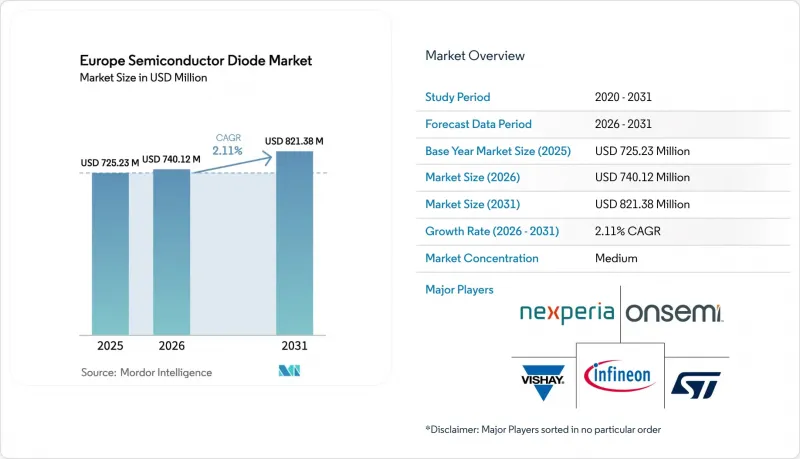
2025 年歐洲半導體二極體市場價值為 7.2523 億美元,預計到 2031 年將達到 8.2138 億美元,而 2026 年為 7.4012 億美元,預測期(2026-2031 年)複合年成長率為 2.11%。
儘管碳化矽 (SiC) 和氮化鎵 (GaN) 在汽車和工業市場佔據主導地位,但傳統矽在注重成本的消費性電子和電信設備市場仍然佔據重要地位,這促使市場逐漸轉向寬能隙材料。德國的大型企劃,例如投資 100 億歐元(116.1 億美元)的 ESMC 晶圓廠和英飛凌的智慧功率晶圓廠,構成了區域產能走廊的基礎,並正在加速 200 毫米 SiC 晶圓的設計和應用。義大利卡塔尼亞產業叢集獲得了 50 億歐元(58 億美元)的資金支持,用於意法半導體 (STMicroelectronics) 的 SiC 裝置生產線,以及 7.3 億歐元(8.4726 億美元)的資金支持,用於其自身的基板生產,這充分體現了《晶片資本法案》的垂直獎勵。儘管肖特基整流器在伺服器電源和電動車車載充電器中仍然扮演著核心角色,但用於 USB4、Thunderbolt 和汽車以太網的暫態電壓抑制器 (TVS) 陣列的成長速度超過了所有其他裝置類型。雖然 2024 年初不斷上漲的電價(197 歐元/兆瓦時)給晶圓廠的利潤率帶來了壓力,但 2025 年 9 月半導體聯盟聲明之後政策的延續性表明,先進節點和寬能隙的投資將迎來進一步的利好。
歐洲半導體二極體市場的趨勢與洞察
電動車的發展正在推動對碳化矽肖特基元件的需求成長。
電池電動車 (BEV) 向 800V 平台的轉變是歐洲對碳化矽 (SiC) 肖特基二極體需求的主要推動力,因為原始設備製造商 (OEM) 正在尋求更快的充電速度和更輕的銅線束。意法半導體 (STMicroelectronics) 已獲得吉利和現代汽車的採用,為其第四代 SOP-2026 封裝的 SiC MOSFET 和肖特基二極體進行共封裝。英飛凌 (Infineon) 的 HybridPACK Drive G3 將於 2024 年底推出,其中整合了 CoolSiC MOSFET 和續流二極體,將應用於德國豪華汽車品牌。預計到 2027 年,卡塔尼亞和沃爾夫斯皮德薩爾蘭工廠向 200 毫米 SiC 晶圓的過渡將使每安培晶片晶圓成本降低 20-25%。然而,歐盟對中國純電動車進口徵收的反補貼關稅(17-35.3%)減緩了短期銷售成長,而獲得 AEC-Q101 0 級認證則使產品上市的前置作業時間延長了 12-18 個月。
利用歐盟晶片技術拓展資金籌措管道
根據《TIPS法案》核准的七座全球首創晶圓廠已獲得總合315億歐元(365.6億美元)的投資,其中三座專門用於寬能隙帶裝置。意法半導體(STMicroelectronics)已投資50億歐元(58億美元)用於擴大其在西西里的裝置產能,並投資7.3億歐元(8.4721億美元)用於其基板業務;安森美半導體(ON Semiconductor)則撥款16.4億歐元(SiCoznov)業務的用於擴大其碳化。由西班牙Imec支持的馬拉加中心,以及已獲批於2026年2月獲得資助的7億歐元NanoIC試點生產線,將使中小企業能夠獲得300毫米工藝,並降低先進節點原型製作的風險。 SEMICON 聯盟提出的「TIPS 法案 2.0」提案預計將在 2028 年前吸引額外 200 億至 300 億歐元(232.1 億至 348.2 億美元)的私人資本。
SiC基板的成本差異:比Si基板高6倍以上。
基板佔成品碳化矽二極體總成本的一半,且價格仍是同等矽晶圓的六倍,阻礙了其廣泛應用。雖然到2027年,從150毫米到200毫米的基板尺寸轉變將使每平方公分的成本降低約20%,但到2031年,其絕對價格仍將是矽的四倍。義法半導體和英飛凌的垂直整合仍是抵禦現貨市場波動的重要保障。
細分市場分析
到2025年,肖特基二極體將佔據歐洲半導體二極體市場43.12%的佔有率,這主要歸功於其小於0.5V的正向壓降,從而提高了電動車充電器和伺服器電源的同步整流效率。齊納二極體和小訊號二極體則用於參考和開關應用,而TVS二極體和ESD陣列的複合年成長率最高,達到2.36%,這主要得益於USB4和車載乙太網路的普及應用。
目前,越來越多的原始設備製造商 (OEM) 指定在 48V 輕混總線中使用氮化鎵 (GaN) TVS,因為與矽基二極體相比,其電容顯著降低。此外,5G 基地台的維修需要反向恢復時間小於 10ns,這也推動了對蕭特基二極體的需求。雖然用於雷射雷達 (LiDAR) 的專用雷射二極體的銷量佔比不到 5%,但 905nm 邊發射設計的需求依然強勁,即便 VCSEL 等替代技術不斷湧現。
預計到2025年,矽將維持其在歐洲半導體二極體市場71.43%的佔有率,這得益於成熟的供應鏈、充足的晶圓產能以及消費者、通訊和低壓行業買家青睞的數十年可靠數據。儘管碳化矽目前仍屬於少數材料,但由於800V牽引逆變器、650V伺服充電器等應用中對開關損耗比矽低30-40%的需求,其市場佔有率預計到2031年將以2.44%的複合年成長率成長。意法半導體(STMicroelectronics)位於卡塔尼亞的工廠計劃到2033年每週生產15,000片200毫米晶圓,而安森美半導體(ON Semiconductor)位於羅茲諾夫的生產線計劃到2027年每年生產40,000片150毫米晶圓。這些發展預計在預測期內將碳化矽在歐洲半導體二極體市場的佔有率擴大到9-10%左右。氮化鎵預計到2025年市佔率僅為3%,但它正在11kW汽車充電器和48V輕混系統的DC-DC轉換器領域站穩腳步。在這些領域,500kHz的開關頻率使得在狹小的引擎室內可以使用更小的電感器並提高功率密度。雖然氧化鎵等新興的超寬頻隙材料仍處於預實用化階段,但歐盟資助的試點生產線(例如NanoIC)已經能夠提供樣品二極體,這些二極體可以在結溫高於200 度C的情況下承受超過3kV的反向偏壓。
垂直整合的趨勢正在重塑成本曲線。義法基板,目標是在2026年前實現40%的碳化矽(SiC)晶圓內部化,從而降低現貨市場波動風險,並將每安培晶片晶圓成本近四分之一。英飛凌(Infineon)在德勒斯登也採取了類似的風險對沖策略,目前正在向200毫米碳化矽生產過渡,同時進行300毫米批次的試生產,為2027年後的大規模量產做準備。像GeneSiC和LittleHughes的子公司這樣不具備自有晶錠製造能力的裝置製造商,正擴大簽訂多年基板供應契約,並轉向氮化鎵(GaN)晶圓,因為氮化鎵晶圓的經濟效益相對較好。矽晶圓在USB電源轉接器、機上盒和消費性電子產品等低電壓應用領域仍可能佔據主導地位。然而,隨著汽車、可再生能源和重工業領域的客戶為了滿足效率要求和降低生命週期成本而將寬能隙整流器標準化,預計到 2031 年,全部區域市場佔有率將下降到 60% 以上。
其他好處:
- Excel格式的市場預測(ME)表
- 3個月的分析師支持
目錄
第1章:引言
- 研究假設和市場定義
- 調查範圍
第2章:調查方法
第3章執行摘要
第4章 市場狀況
- 市場概覽
- 市場促進因素
- SiC-肖特基技術的普及化是由電動車的發展所推動的。
- 透過歐盟晶片法擴大融資管道
- 5G/FTTx整流器更換週期
- GaN TVS設計在電動車車載充電器的應用記錄
- 適用於高功率低於 3kW 的資料中心的電源單元 (PSU)
- 650V以下邊緣AI工業驅動器
- 市場限制因素
- SiC基板的成本(與Si相比)超過6倍。
- 汽車OEM廠商的PPAP積壓訂單不到18個月。
- 歐盟能源價格波動對製造營運成本的影響
- 對進口中國製造的純電動車徵收貿易減免關稅。
- 產業價值鏈分析
- 監理情勢
- 技術展望
- 宏觀經濟因素對市場的影響
- 波特五力分析
- 供應商的議價能力
- 買方的議價能力
- 新進入者的威脅
- 替代品的威脅
- 競爭公司之間的競爭
第5章 市場規模與成長預測
- 按類型
- 肖特基
- 齊納
- TVS/ESD
- 雷射
- 小訊號切換
- 其他類型
- 按基板
- 矽(Si)
- 碳化矽(SiC)
- 氮化鎵(GaN)
- 其他基板
- 按最終用途行業分類
- 汽車和交通運輸
- 家用電子電器
- 通訊基礎設施
- 工業自動化和電力
- 計算和資料中心
- 其他終端用戶產業
- 透過使用
- 功率整流和轉換
- 電壓調節與參考電壓
- 靜電/突波/電路保護
- 其他用途
- 按包裝類型
- 表面黏著技術(SMD)
- 通孔
- 國家
- 德國
- 英國
- 法國
- 義大利
- 西班牙
- 其他歐洲地區
第6章 競爭情勢
- 公司簡介
- Infineon Technologies AG
- STMicroelectronics NV
- Nexperia BV
- Vishay Intertechnology, Inc.
- onsemi Corporation
- ROHM Co., Ltd.
- Littelfuse, Inc.
- Toshiba Electronic Devices and Storage Corp.
- Renesas Electronics Corp.
- Hitachi Power Semiconductor Device Ltd.
- Mitsubishi Electric Corp.
- Microchip Technology Inc.
- Central Semiconductor Corp.
- WeEn Semiconductors
- Semikron Danfoss
- GeneSiC Semiconductor
- ABB Semiconductors
- Diotec Semiconductor AG
- IXYS(Littelfuse)
- Wolfspeed, Inc.
第7章 市場機會與未來展望
The Europe Semiconductor Diode Market size was valued at USD 725.23 million in 2025 and is estimated to grow from USD 740.12 million in 2026 to reach USD 821.38 million by 2031, at a CAGR of 2.11% during the forecast period (2026-2031).
A gradual pivot toward wide-bandgap materials is unfolding as silicon carbide (SiC) and gallium nitride (GaN) capture automotive and industrial sockets, while legacy silicon remains entrenched in cost-sensitive consumer and telecom gear. Germany's public-private megaprojects, including the EUR 10 billion (USD 11.61 billion) ESMC fab and Infineon's Smart Power Fab, are anchoring regional capacity corridors and stimulating design-in activity for 200 mm SiC wafers. Italy's Catania cluster, backed by EUR 5 billion (USD 5.80 billion) for STMicroelectronics' SiC device line and EUR 730 million (USD 847.26 million) for captive substrate output, demonstrates how Chips Act incentives funnel capital toward vertical integration. Schottky rectifiers keep their central role in server power supplies and EV on-board chargers, yet transient-voltage-suppression (TVS) arrays for USB4, Thunderbolt and automotive Ethernet outpace all other device classes. Elevated electricity tariffs 197 EUR/MWh in early 2024 squeeze fab margins, but policy continuity after the September 2025 Semicon Coalition declaration signals further tailwinds for advanced-node and wide-bandgap investment.
Europe Semiconductor Diode Market Trends and Insights
E-Mobility Led SiC-Schottky Pull-Through
Battery-electric vehicles moving to 800 V platforms are the prime catalyst for SiC Schottky demand in Europe, as OEMs seek faster charging and lighter copper harnesses. STMicroelectronics logged design wins with Geely and Hyundai for fourth-generation SiC MOSFETs co-packaged with Schottky diodes for SOP-2026 lines. Infineon's HybridPACK Drive G3, rolled out in late 2024, integrates CoolSiC MOSFETs and free-wheeling diodes for German premium brands. Transitioning to 200 mm SiC wafers at Catania and Wolfspeed Saarland is expected to trim die cost per ampere by 20-25% by 2027. Yet EU anti-subsidy duties of 17-35.3% on Chinese BEV imports have softened near-term unit pull-through, and AEC-Q101 Grade 0 validation pushes product-launch lead-times out by 12-18 months.
Expansion of EU Chips Act Funding Pipeline
Seven first-of-a-kind fabs approved under the Chips Act have secured EUR 31.5 billion (USD 36.56 billion) in combined spending, with three dedicated to wide-bandgap devices. STMicroelectronics alone commands EUR 5 billion (USD 5.80 billion) for device capacity and EUR 730 million (USD 847.21 million) for substrates in Sicily, while onsemi allocates EUR 1.64 billion (USD 1.90 billion) to Roznov SiC expansion. Spain's Imec-backed Malaga center and the EUR 700 million NanoIC pilot line, funded in February 2026, give SMEs 300 mm access and de-risk advanced-node prototyping. The Semicon Coalition's call for a "Chips Act 2.0" could unlock another EUR 20-30 billion (USD 23.21 -34.82 billion) in private capital by 2028.
SiC Substrate Cost Delta vs. Si Greater Than 6X
Substrates account for half of finished SiC diode cost and still price out at six times equivalent silicon wafers, hindering broader penetration. Moving from 150 mm to 200 mm cuts cost per square centimeter by roughly 20% by 2027, yet the absolute premium stays quadruple that of silicon through 2031. Vertical integration at STMicro and Infineon remains the chief hedge against volatile spot markets.
Other drivers and restraints analyzed in the detailed report include:
- Telecom 5G / FTTx Rectifier Renewal
- EV On-Board Charger Design-Wins for GaN TVS
- Automotive OEM PPAP Backlog Less Than18 Months
For complete list of drivers and restraints, kindly check the Table Of Contents.
Segment Analysis
Schottky devices represented 43.12% of the Europe semiconductor diode market size in 2025, a share rooted in their sub-0.5 V forward drop that improves synchronous rectifier efficiency in EV chargers and server PSUs. Zener and small-signal diodes serve as references and for switching, while TVS and ESD arrays post the steepest 2.36% CAGR thanks to USB4 and automotive Ethernet rollouts.
More OEMs now specify GaN TVS for 48 V mild-hybrid buses, citing order-of-magnitude lower capacitance than silicon counterparts. Schottky demand also benefits from 5G base-station retrofits that require less than 10 ns of reverse recovery time. Niche laser diodes for LiDAR contribute under 5% of revenue but see solid traction in 905 nm edge-emitting designs, even as VCSEL alternatives loom.
Silicon retained 71.43% Europe semiconductor diode market share in 2025, underpinned by its mature supply chain, abundant wafer capacity and decades-long reliability data favored by consumer, telecom and low-voltage industrial buyers. Silicon carbide, though still a minority material, is pacing a 2.44% CAGR to 2031 as 800 V traction inverters, 650 V servo drives and 350 kW grid-scale battery chargers demand 30-40% lower switching losses than silicon can deliver. STMicroelectronics' Catania hub targets 15,000 200 mm wafers per week by 2033, while onsemi's Roznov line will push 40,000 150 mm wafers annually by 2027, moves that could lift SiC's slice of the Europe semiconductor diode market size toward 9-10% over the forecast horizon. Gallium nitride, holding barely 3% volume in 2025, is carving footholds in 11 kW on-board chargers and 48 V mild-hybrid DC-DC converters, where 500 kHz switching shrinks inductors and raises power density in cramped engine bays. Emerging ultra-wide-bandgap options such as gallium oxide remain pre-commercial, but EU-funded pilot lines like NanoIC are sampling demonstrator diodes that withstand over 3 kV reverse bias at junction temperatures above 200 °C.
Vertical-integration plays are rewriting cost curves: STMicroelectronics' EUR 730 million captive-substrate project seeks to internalize 40% of its SiC wafer demand by 2026, cutting exposure to spot-market swings and shaving die cost per ampere by nearly one-quarter. Infineon pursues a similar hedge at Dresden, shifting to 200 mm SiC production today and piloting 300 mm lots for post-2027 ramps. Device makers without in-house boule capacity, including GeneSiC and Littelfuse subsidiaries, increasingly lock multi-year substrate supply contracts or pivot toward GaN where wafer economics are comparatively benign. Silicon will still dominate low-voltage sockets USB power bricks, set-top boxes, home appliances-yet its region-wide share is likely to dip to the high-sixties by 2031 as automotive, renewable-energy and heavy-industry clients standardize on wide-bandgap rectifiers for efficiency mandates and lifetime cost reductions.
The Europe Semiconductor Diode Market Report is Segmented by Type (Schottky, Zener, and More), Base Material (Silicon, Silicon Carbide, and More), End-Use Industry (Automotive and Transportation, Consumer Electronics, and More), Application (Power Rectification and Conversion, and More), Package Type (Surface Mount, and Through-Hole), and Country (Germany, and More). The Market Forecasts are Provided in Terms of Value (USD).
List of Companies Covered in this Report:
- Infineon Technologies AG
- STMicroelectronics N.V.
- Nexperia B.V.
- Vishay Intertechnology, Inc.
- onsemi Corporation
- ROHM Co., Ltd.
- Littelfuse, Inc.
- Toshiba Electronic Devices and Storage Corp.
- Renesas Electronics Corp.
- Hitachi Power Semiconductor Device Ltd.
- Mitsubishi Electric Corp.
- Microchip Technology Inc.
- Central Semiconductor Corp.
- WeEn Semiconductors
- Semikron Danfoss
- GeneSiC Semiconductor
- ABB Semiconductors
- Diotec Semiconductor AG
- IXYS (Littelfuse)
- Wolfspeed, Inc.
Additional Benefits:
- The market estimate (ME) sheet in Excel format
- 3 months of analyst support
TABLE OF CONTENTS
1 INTRODUCTION
- 1.1 Study Assumptions and Market Definition
- 1.2 Scope of the Study
2 RESEARCH METHODOLOGY
3 EXECUTIVE SUMMARY
4 MARKET LANDSCAPE
- 4.1 Market Overview
- 4.2 Market Drivers
- 4.2.1 E-Mobility Led SiC-Schottky Pull-Through
- 4.2.2 Expansion of EU Chips Act Funding Pipeline
- 4.2.3 Telecom 5G / FTTx Rectifier Replacement Cycle
- 4.2.4 EV On-Board Charger Design-Wins for GaN TVS
- 4.2.5 Power-Dense Data-Centre PSUs Less Than 3 kW
- 4.2.6 Edge-AI Industrial Drives Less Than 650 V
- 4.3 Market Restraints
- 4.3.1 SiC Substrate Cost Delta vs. Si Greater Than 6x
- 4.3.2 Automotive OEM PPAP Backlog Less Than 18 Months
- 4.3.3 EU Energy-Price Volatility on Fab OPEX
- 4.3.4 Trade-Remedy Tariffs on Chinese BEV Imports
- 4.4 Industry Value Chain Analysis
- 4.5 Regulatory Landscape
- 4.6 Technological Outlook
- 4.7 Impact of Macroeconomic Factors on the Market
- 4.8 Porter's Five Forces Analysis
- 4.8.1 Bargaining Power of Suppliers
- 4.8.2 Bargaining Power of Buyers
- 4.8.3 Threat of New Entrants
- 4.8.4 Threat of Substitutes
- 4.8.5 Intensity of Competitive Rivalry
5 MARKET SIZE AND GROWTH FORECASTS (VALUE)
- 5.1 By Type
- 5.1.1 Schottky
- 5.1.2 Zener
- 5.1.3 TVS / ESD
- 5.1.4 Laser
- 5.1.5 Small-Signal Switching
- 5.1.6 Other Types
- 5.2 By Base Material
- 5.2.1 Silicon (Si)
- 5.2.2 Silicon Carbide (SiC)
- 5.2.3 Gallium Nitride (GaN)
- 5.2.4 Other Base Materials
- 5.3 By End-Use Industry
- 5.3.1 Automotive and Transportation
- 5.3.2 Consumer Electronics
- 5.3.3 Communications Infrastructure
- 5.3.4 Industrial Automation and Power
- 5.3.5 Computing and Data Centre
- 5.3.6 Other End-Use Industries
- 5.4 By Application
- 5.4.1 Power Rectification and Conversion
- 5.4.2 Voltage Regulation and Reference
- 5.4.3 Electrostatic / Surge / Circuit Protection
- 5.4.4 Other Applications
- 5.5 By Package Type
- 5.5.1 Surface Mount (SMD)
- 5.5.2 Through-Hole
- 5.6 By Country
- 5.6.1 Germany
- 5.6.2 United Kingdom
- 5.6.3 France
- 5.6.4 Italy
- 5.6.5 Spain
- 5.6.6 Rest of Europe
6 COMPETITIVE LANDSCAPE
- 6.1 Company Profiles (includes Global Level Overview, Market Level Overview, Core Segments, Financials as Available, Strategic Information, Market Rank / Share, Products and Services, Recent Developments)
- 6.1.1 Infineon Technologies AG
- 6.1.2 STMicroelectronics N.V.
- 6.1.3 Nexperia B.V.
- 6.1.4 Vishay Intertechnology, Inc.
- 6.1.5 onsemi Corporation
- 6.1.6 ROHM Co., Ltd.
- 6.1.7 Littelfuse, Inc.
- 6.1.8 Toshiba Electronic Devices and Storage Corp.
- 6.1.9 Renesas Electronics Corp.
- 6.1.10 Hitachi Power Semiconductor Device Ltd.
- 6.1.11 Mitsubishi Electric Corp.
- 6.1.12 Microchip Technology Inc.
- 6.1.13 Central Semiconductor Corp.
- 6.1.14 WeEn Semiconductors
- 6.1.15 Semikron Danfoss
- 6.1.16 GeneSiC Semiconductor
- 6.1.17 ABB Semiconductors
- 6.1.18 Diotec Semiconductor AG
- 6.1.19 IXYS (Littelfuse)
- 6.1.20 Wolfspeed, Inc.
7 MARKET OPPORTUNITIES AND FUTURE OUTLOOK
- 7.1 White-Space and Unmet-Need Assessment
 半導體及相關裝置市場:全球產業分析、市場規模、市場佔有率及預測(2026-2033 年),依半導體類型、裝置類型、材料類型、技術、應用、國家及地區分類
 2026-2030年全球半導體市場
 有機半導體市場:全球產業規模、市場佔有率、趨勢、機會和預測(按材料類型、應用和地區分類)、競爭格局(2021-2031 年)
 智慧電網半導體元件市場預測至2034年:按元件、應用、最終用戶和地區分類的全球分析金屬氧化物半導體電路市場報告:趨勢、預測與競爭分析(至2035年)
 直接寫入式半導體市場規模、佔有率和成長分析:按技術/設備類型、材料類型、應用和地區分類-2026-2033年產業預測
 用於替代能源技術的半導體:機會和市場SIM卡、SIM晶片和eSIM市場數據概覽:2026年第二季度
 半導體擴散設備市場規模、佔有率和趨勢分析報告:按產品、技術、應用、晶圓尺寸、地區和細分市場分類(2026-2033 年)人工智慧半導體市場預測至2034年—按類型、應用、最終用戶和地區分類的全球分析