


 |
市場調查報告書
商品編碼
2044014
人工智慧和高效能運算半導體矽晶圓:市場佔有率分析、產業趨勢和統計數據以及成長預測(2026-2031 年)AI And HPC Semiconductor Silicon Wafer - Market Share Analysis, Industry Trends & Statistics, Growth Forecasts (2026 - 2031) |
||||||
※ 本網頁內容可能與最新版本有所差異。詳細情況請與我們聯繫。
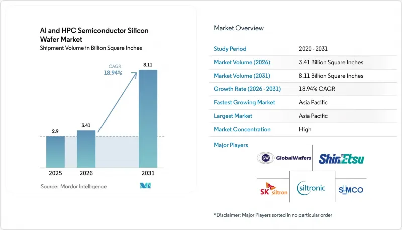
預計人工智慧和高效能運算半導體矽晶圓的市場規模將從 2025 年的 29 億平方英寸和 2026 年的 34.1 億平方英寸成長到 2031 年的 81.1 億平方英寸,2026 年至 2031 年的年複合成長率(CAGR)為 18.94%。
確保3奈米以下邏輯晶圓的產能、與政府補貼計劃掛鉤的多年期契約,以及向專為推理最佳化的加速器轉型,共同推動了市場需求的成長。在台灣、韓國、美國和中國,300毫米晶圓生產線的擴張速度超過了晶體提取設備的交付速度,導致現貨市場供應緊張,並推高了合約價格。華盛頓、布魯塞爾和北京的平行補貼計畫促進了地域均衡的投資,這意味著亞洲晶圓代工廠不再將西方同行拒之門外。綜上所述,這些因素使晶圓平整度和缺陷密度領先的行業領先供應商在未來十年內擁有結構性優勢,並有望實現高利潤率。
全球人工智慧與高效能運算半導體矽晶圓市場趨勢與洞察
人工智慧加速器對300毫米晶圓的需求激增
超大規模業者在2025年採購了120萬張加速卡,每張加速卡在300毫米基板上佔用高達1200平方毫米的矽晶圓,其占地面積比通用CPU大40%。晶片基板(CoWS)技術使每個GPU的晶圓使用量翻倍,因為多個晶片(受反光晶圓限制)共用單一中介層。微軟和Meta計劃在2026年推出各自的3奈米推理處理器,將進一步加劇市場需求。由於200毫米基板在先進邏輯電路中的經濟性過時,生產正集中到300毫米生產線上,該生產線可以將總厚度偏差控制在0.15微米以下。目前,全球只有不到五家供應商能夠滿足這項精確度要求,這將使寡占定價權在整個預測期內得以維持。
台灣及美國7奈米以下晶圓代工廠快速擴張
台積電已投資650億美元擴建其位於亞利桑那州的工廠,該工廠已於2025年12月開始出貨4奈米工程晶圓。三星平澤園區新增了第五間潔淨室,用於生產2奈米環柵(GaAA)裝置,該裝置計畫於2026年中期開始量產。英特爾位於俄亥俄州的計畫預計於2027年採用18A製程實現每月6萬片晶圓的產能。光是這三個項目到2028年就將新增每月30萬片晶圓的產能,但由於設備瓶頸,全面投產預計將延遲12至18個月。因此,台灣在7奈米以下製程產能的佔有率將從2023年的92%下降到2027年的約78%。這將分散地緣政治風險,但由於各司法管轄區的出口限制,跨境物流也將變得更加複雜,從而造成摩擦。
超高純度多晶矽供應鏈中的脆弱性
預計到2025年,七家公司將生產幾乎全部的半導體多晶矽,其中瓦克半導體、海姆洛克半導體和德山半導體將佔總產量的65%。屆時,太陽能需求將推動現貨價格從每公斤28美元上漲至41美元。美國對強迫勞動的限制將導致新疆生產停止,造成4萬噸產能損失。德山半導體在沙撈越的擴建工程將於2026年中期新增1萬噸產能,但需18個月的認證期。因此,沒有長期合約的中小型晶圓製造商正面臨原料發行,如果這種情況得不到緩解,可能會使預期的複合年成長率下降近兩個百分點。
細分市場分析
到2025年,人工智慧和高效能運算半導體矽晶圓市場中,300mm晶圓將佔據94.64%的市場佔有率,這得益於其卓越的晶片良率帶來的經濟優勢。 300mm晶圓的有效面積約為200mm基板的2.4倍,可將每個電晶體的製造成本降低30-40%。諸如台積電的CoWoS等晶圓代工廠封裝流程僅支援300mm中介層,因此將超大規模企業限制在此直徑範圍內。英特爾即將推出的背面電源架構對總厚度的公差要求嚴格,僅有0.12µm,這是傳統200mm製造設備無法達到的。因此,掌握超平坦300mm晶圓製造技術的供應商正成為所有先進邏輯晶圓廠的首選供應商。
隨著超大規模資料中心業者計劃在2026年後採用3奈米製程製程生產客製化推理晶片,這種成長勢頭不太可能放緩。因此,該細分市場的複合年成長率(CAGR)高達19.68%,超過了以平方英吋計的整體人工智慧和高效能運算半導體矽晶圓市場規模。同時,受FD-SOI和碳化矽(SiC)等晶片尺寸較小的應用推動,對200毫米晶圓的需求正穩定成長。設備供應商正逐步淘汰150毫米晶圓服務,迫使老牌晶圓廠要麼轉型,要麼退出市場,加速了產業重組。近期的一些併購交易,例如GlobalWafers收購Siltronic在新加坡的資產,已將中國以外超過四分之一的300毫米晶圓產能整合到單一所有者手中,重塑了晶圓代工廠客戶的議價動態。
《人工智慧和高效能運算半導體矽晶圓市場報告》按晶圓直徑(300毫米和200毫米)、技術節點(先進節點、主流節點、成熟節點)和地區進行細分。市場預測以體積(平方英吋)為單位。
區域分析
預計到2025年,亞太地區將佔據74.62%的市場佔有率,並以每年19.82%的速度成長至2031年。光是台積電一家在台灣每月就消耗80萬片晶圓,而其位於日本熊本的新廠預計將在2026年下半年新增5.5萬片晶圓的產能。三星平澤園區的P4生產線於2025年運作後,月產能已達40萬片晶圓。中國已在上游材料領域投資1,500億元人民幣,目標是到2025年將國產晶圓採購率提高到32%,以取代進口晶圓,儘管國產晶圓的缺陷密度存在差異。日本已獲得4兆日圓(約270億美元)的補貼,以避免過度依賴台灣,加劇了區域間對技術純熟勞工的競爭。
儘管規模較小,但在《晶片創新與生產法案》(CHIPS Act)的獎勵下,北美地區正在迅速擴張。英特爾位於亞利桑那州和俄亥俄州的工廠預計到2028年將開始每月生產12萬片晶圓,而台積電位於鳳凰城的工廠已經開始出貨4奈米矽晶圓。 Global Wafers公司已在德克薩斯州謝爾曼市啟動了一座價值50億美元的工廠建設,目標是每年生產120萬片晶圓。水資源短缺正成為阻礙因素;亞利桑那州的工廠每天用水量高達400萬加侖,迫使監管機構強制要求90%的用水再利用率,目前只有台積電達到了這一目標。實現永續的用水效率將是未來獲得獎勵付款的關鍵條件。
到2025年,歐洲將佔全球半導體產量的8%(以平方英吋計算),主要集中在汽車和功率元件領域。英飛凌的德勒斯登工廠和義法半導體的克羅爾工廠均從Siltronic的弗賴貝格工廠採購晶圓,以滿足《晶片法》的在地採購要求。博世在羅伊特林根新增了一條200毫米晶圓生產線,以緩解汽車感測器短缺的問題,但其尖端邏輯裝置仍依賴進口。南美和中東及非洲地區的總產量不足全球總產量的2%,且缺乏優質的晶圓製造設施,因此,當亞太地區的物流緊張時,當地的組裝很容易受到運輸和關稅突變的影響。
其他好處:
- Excel格式的市場預測(ME)表
- 3個月的分析師支持
目錄
第1章:引言
- 研究假設和市場定義
- 調查範圍
第2章:調查方法
第3章執行摘要
第4章 市場狀況
- 市場概覽
- 市場促進因素
- 人工智慧加速器對 300 毫米晶圓的需求正在激增。
- 台灣及美國7奈米以下晶圓代工廠快速擴張
- 加大對中國晶圓製造業企業的資金支持
- 先進高效能運算GPU的激進節點小型化
- 採用背面供電和晶圓級鍵合技術
- 促進優質晶圓回收利用的永續性要求
- 市場限制因素
- 超高純度多晶矽供應鏈中的脆弱性
- 晶體繪製設備的前置作業時間很長。
- 高昂的資本投資成本限制了新進入者的數量。
- 大型晶圓廠面臨水和電力短缺的風險
- 產業供應鏈分析
- 監理情勢
- 技術展望
- 宏觀經濟因素對市場的影響
- 波特五力分析
- 新進入者的威脅
- 供應商的議價能力
- 買方的議價能力
- 替代品的威脅
- 競爭公司之間的競爭
第5章 市場規模與成長預測
- 依晶圓直徑
- 300 mm
- 200 mm
- 依技術節點
- 先進節點(小於7奈米)
- 主流製程(10nm 至 28nm)
- 成熟節點(28nm以上)
- 按地區
- 北美洲
- 美國
- 加拿大
- 墨西哥
- 歐洲
- 德國
- 英國
- 法國
- 其他歐洲地區
- 亞太地區
- 中國
- 日本
- 印度
- 韓國
- 台灣
- 亞太其他地區
- 南美洲
- 中東和非洲
- 北美洲
第6章 競爭情勢
- 市場集中度
- 策略趨勢
- 市佔率分析
- 公司簡介
- Shin-Etsu Chemical Co., Ltd.
- Sumco Corporation
- GlobalWafers Co., Ltd.
- Siltronic AG
- SK Siltron Co., Ltd.
- Wafer Works Corporation
- Soitec SA
- Okmetic Oyj
- Sil'tronix Silicon Technologies
- Shanghai Simgui Technology Co., Ltd.
- Zhejiang Jinruihong Silicon Material Co., Ltd.
- Episil-Precision Inc.
- Poshing Technology Co., Ltd.
- Heraeus Holding GmbH
- LG Siltron Inc.
- Tokuyama Corporation
- Ferrotec Holdings Corporation
- AXT, Inc.
第7章 市場機會與未來展望
The AI and HPC semiconductor silicon wafer market size is projected to expand from 2.9 billion square inches in 2025 and 3.41 billion square inches in 2026 to 8.11 billion square inches by 2031, registering a CAGR of 18.94% between 2026 to 2031.
Capacity secured for sub-3-nanometer logic, multi-year offtake deals tied to sovereign subsidy programs, and the migration toward inference-optimized accelerators collectively reinforce demand momentum. Taiwan, South Korea, the United States, and China are expanding 300 millimeter lines faster than crystal-pulling equipment can be delivered, tightening spot availability and lifting contract prices. Asian foundries no longer crowd out Western peers, because parallel subsidy corridors in Washington, Brussels, and Beijing have seeded geographically balanced investments. Taken together, these factors position wafer suppliers with flatness and defect-density leadership to capture structurally higher margins through the decade.
Global AI And HPC Semiconductor Silicon Wafer Market Trends and Insights
Surging Demand for 300mm Wafers in AI Accelerators
Hyperscale operators purchased 1.2 million accelerator cards in 2025, with each unit consuming up to 1,200 mm2 of silicon on 300 millimeter substrates, a footprint 40% larger than general-purpose CPUs. Chip-on-wafer-on-substrate packaging doubles wafer usage per GPU because multiple reticle-limited dies share a single interposer. Transition plans by Microsoft and Meta to launch proprietary 3 nanometer inference processors in 2026 further lift demand pressure. The economic obsolescence of 200 millimeter substrates for leading-edge logic concentrates volume on 300 millimeter lines that can hold total-thickness variation below 0.15 µm. Fewer than five global suppliers currently meet that tolerance, which preserves oligopolistic pricing power through the forecast horizon.
Rapid Foundry Expansions Below 7nm in Taiwan and the United States
TSMC committed USD 65 billion to Arizona plants that began shipping 4 nanometer engineering wafers in December 2025. Samsung's Pyeongtaek campus added a fifth cleanroom for 2 nanometer gate-all-around devices slated for mid-2026 volume. Intel's Ohio project will reach 60,000 wafer starts per month on 18A in 2027. These three programs alone add 300,000 starts monthly by 2028, though equipment bottlenecks push full output 12-18 months to the right. Taiwan's share of sub-7 nanometer capacity therefore declines from 92% in 2023 to roughly 78% in 2027, diffusing geopolitical risk but introducing jurisdictional export-control frictions that complicate cross-border logistics.
Supply Chain Fragility for Ultrapure Polysilicon
Seven firms produced nearly all semiconductor-grade polysilicon in 2025, with Wacker, Hemlock, and Tokuyama covering 65%. Solar demand lifted spot prices from USD 28/kg to USD 41/kg during the year. U.S. forced-labor rules blocked Xinjiang origin, removing 40,000 t of capacity. Tokuyama's Sarawak expansion adds 10,000 t in mid-2026 but needs 18 months of qualification. Smaller wafer houses without long contracts therefore face feedstock rationing, which could shave nearly 2 percentage points off the forecast CAGR if unmitigated.
Other drivers and restraints analyzed in the detailed report include:
- Growing Capital Support for Domestic Wafer Fabs in China
- Aggressive Node Shrinks for Advanced HPC GPUs
- Long Lead Times on Crystal-Pulling Equipment
For complete list of drivers and restraints, kindly check the Table Of Contents.
Segment Analysis
The 300 mm segment of the AI and HPC semiconductor silicon wafer market accounted for 94.64% of the market share in 2025, reflecting its superior die-yield economics. Every 300 millimeter disk offers roughly 2.4X usable area versus a 200 millimeter substrate, reducing manufacturing expense per transistor by 30-40%. Foundry packaging flows, such as TSMC CoWoS, only accept 300 millimeter interposers, which lock hyperscale buyers into this diameter. Intel's upcoming backside power architecture tightens total-thickness budgets to 0.12 µm, a figure unreachable on legacy 200 millimeter tools. Consequently, suppliers that master ultra-flat 300 millimeter crystals hold preferred-vendor status at all advanced logic fabs.
Growth momentum is unlikely to abate, as hyperscalers plan to produce custom inference chips on 3-nanometer nodes from 2026 onward. The segment's 19.68% CAGR, therefore, exceeds the broader AI and HPC semiconductor silicon wafer market size trajectory as measured in square inches. Conversely, demand for 200 millimeter wafers is growing steadily, driven by FD-SOI and silicon-carbide applications where die sizes remain small. Equipment vendors have begun to sunset 150 millimeter service, forcing older fabs either to migrate or exit, a trend that accelerates consolidation. Recent M&A, such as GlobalWafers acquiring Siltronic's Singapore asset, places more than one-quarter of non-Chinese 300 millimeter capacity under one owner, reshaping bargaining dynamics with foundry customers.
The AI and HPC Semiconductor Silicon Wafer Market Report is Segmented by Wafer Diameter (300mm and 200mm), Technology Node (Advanced Node, Mainstream Node, and Mature Node), and Geography. The Market Forecasts are Provided in Terms of Volume (Square Inches).
Geography Analysis
Asia-Pacific retained 74.62% of the market share in 2025 and is forecast to advance at 19.82% through 2031. TSMC alone consumed 800,000 starts per month across Taiwan, while its new Kumamoto plant in Japan adds 55,000 starts in late 2026. Samsung's Pyeongtaek campus reached 400,000 starts monthly after the P4 line came online in 2025. China lifted domestic wafer sourcing to 32% by 2025, substituting imports despite defect-density disparities, and poured RMB 150 billion into upstream materials. Japan attracted JPY 4 trillion (USD 27 billion) in subsidies that hedge against Taiwan concentration, raising regional competition for skilled labor.
North America, though smaller, expands rapidly under CHIPS Act incentives. Intel's Arizona and Ohio sites will draw 120,000 starts monthly by 2028, while TSMC's Phoenix module already ships 4 nanometer silicon. GlobalWafers broke ground on a USD 5 billion Sherman, Texas plant, aiming for 1.2 million wafers annually. Water scarcity surfaced as a binding constraint, with Arizona fabs consuming 4 million gallons daily, prompting regulators to mandate 90% reuse targets that only TSMC currently meets. Achieving sustainable water intensity is now a gating factor for future incentive disbursements.
Europe captured 8% of global square-inch output in 2025, specializing in automotive and power devices. Infineon's Dresden fab and STMicroelectronics' Crolles site pull wafers from Siltronic's Freiberg plant to satisfy Chips Act local-content rules. Bosch added a 200 millimeter line in Reutlingen to ease vehicle-sensor shortages but remains reliant on imports for leading-edge logic. South America and the Middle East and Africa together account for less than 2% of volume and host no prime-wafer facilities, exposing local assemblers to shipping and tariff shocks when Asia-Pacific logistics tighten.
- Shin-Etsu Chemical Co., Ltd.
- Sumco Corporation
- GlobalWafers Co., Ltd.
- Siltronic AG
- SK Siltron Co., Ltd.
- Wafer Works Corporation
- Soitec S.A.
- Okmetic Oyj
- Sil'tronix Silicon Technologies
- Shanghai Simgui Technology Co., Ltd.
- Zhejiang Jinruihong Silicon Material Co., Ltd.
- Episil-Precision Inc.
- Poshing Technology Co., Ltd.
- Heraeus Holding GmbH
- LG Siltron Inc.
- Tokuyama Corporation
- Ferrotec Holdings Corporation
- AXT, Inc.
Additional Benefits:
- The market estimate (ME) sheet in Excel format
- 3 months of analyst support
TABLE OF CONTENTS
1 INTRODUCTION
- 1.1 Study Assumptions and Market Definition
- 1.2 Scope of the Study
2 RESEARCH METHODOLOGY
3 EXECUTIVE SUMMARY
4 MARKET LANDSCAPE
- 4.1 Market Overview
- 4.2 Market Drivers
- 4.2.1 Surging Demand for 300 Mm Wafers in AI Accelerators
- 4.2.2 Rapid Foundry Expansions Below 7 Nm in Taiwan and the United States
- 4.2.3 Growing Capital Support for Domestic Wafer Fabs in China
- 4.2.4 Aggressive Node Shrinks for Advanced HPC GPUs
- 4.2.5 Adoption of Backside-Power Delivery and Wafer-Level Bonding
- 4.2.6 Sustainability Mandates Driving Prime Wafer Recycling
- 4.3 Market Restraints
- 4.3.1 Supply Chain Fragility for Ultrapure Polysilicon
- 4.3.2 Long Lead Times on Crystal-Pulling Equipment
- 4.3.3 High Capex Intensity Limiting New Entrants
- 4.3.4 Water and Power Scarcity Risks at Mega-Fabs
- 4.4 Industry Supply-Chain Analysis
- 4.5 Regulatory Landscape
- 4.6 Technological Outlook
- 4.7 Impact of Macroeconomic Factors on the Market
- 4.8 Porter's Five Forces Analysis
- 4.8.1 Threat of New Entrants
- 4.8.2 Bargaining Power of Suppliers
- 4.8.3 Bargaining Power of Buyers
- 4.8.4 Threat of Substitutes
- 4.8.5 Intensity of Competitive Rivalry
5 MARKET SIZE AND GROWTH FORECASTS (VOLUME)
- 5.1 By Wafer Diameter
- 5.1.1 300 mm
- 5.1.2 200 mm
- 5.2 By Technology Node
- 5.2.1 Advanced Node (Below 7nm)
- 5.2.2 Mainstream Node (10nm-28nm)
- 5.2.3 Mature Node (Above 28nm)
- 5.3 By Geography
- 5.3.1 North America
- 5.3.1.1 United States
- 5.3.1.2 Canada
- 5.3.1.3 Mexico
- 5.3.2 Europe
- 5.3.2.1 Germany
- 5.3.2.2 United Kingdom
- 5.3.2.3 France
- 5.3.2.4 Rest of Europe
- 5.3.3 Asia-Pacific
- 5.3.3.1 China
- 5.3.3.2 Japan
- 5.3.3.3 India
- 5.3.3.4 South Korea
- 5.3.3.5 Taiwan
- 5.3.3.6 Rest of Asia-Pacific
- 5.3.4 South America
- 5.3.5 Middle East and Africa
- 5.3.1 North America
6 COMPETITIVE LANDSCAPE
- 6.1 Market Concentration
- 6.2 Strategic Moves
- 6.3 Market Share Analysis
- 6.4 Company Profiles (includes Global level Overview, Market Level Overview, Core Segments, Financials as Available, Strategic Information, Market Rank/Share for Key Companies, Products and Services, and Recent Developments)
- 6.4.1 Shin-Etsu Chemical Co., Ltd.
- 6.4.2 Sumco Corporation
- 6.4.3 GlobalWafers Co., Ltd.
- 6.4.4 Siltronic AG
- 6.4.5 SK Siltron Co., Ltd.
- 6.4.6 Wafer Works Corporation
- 6.4.7 Soitec S.A.
- 6.4.8 Okmetic Oyj
- 6.4.9 Sil'tronix Silicon Technologies
- 6.4.10 Shanghai Simgui Technology Co., Ltd.
- 6.4.11 Zhejiang Jinruihong Silicon Material Co., Ltd.
- 6.4.12 Episil-Precision Inc.
- 6.4.13 Poshing Technology Co., Ltd.
- 6.4.14 Heraeus Holding GmbH
- 6.4.15 LG Siltron Inc.
- 6.4.16 Tokuyama Corporation
- 6.4.17 Ferrotec Holdings Corporation
- 6.4.18 AXT, Inc.
7 MARKET OPPORTUNITIES AND FUTURE OUTLOOK
- 7.1 White-Space and Unmet-Need Assessment
 2026年全球量子模擬器市場報告2026年全球多模態記憶體市場報告2026 年 AI 工作負載的 RoCE(基於融合乙太網路的 RDMA)全球市場報告
 伺服器和高效能運算用ABF基板市場:按應用、材料類型、層數和基板厚度分類,全球預測,2026-2032年
 全球智慧自動化測試市場:預測至 2032 年 - 按組件、測試類型、部署方法、組織規模、介面、最終用戶和地區進行分析全球人工智慧微型倉配市場預測(至 2032 年):按組件、部署模型、公司規模、技術、應用、最終用戶和地區進行分析
 2025 年至 2029 年全球 AI 增強型 HPC 市場
 MRDIMM 伺服器記憶體展望:推動 AI 和 HPC 趨勢
 人工智慧增強型 HPC 全球市場報告:趨勢、預測和競爭分析(至 2031 年)
 全球 AI 增強型 HPC 市場規模研究,按組件、計算類型(平行計算、分散式計算和百億億次計算)、產業、部署、伺服器價格區間和區域預測 2022-2032