


 |
市場調查報告書
商品編碼
2044008
消費性電子產品用半導體矽晶圓:市場佔有率分析、產業趨勢與統計數據以及成長預測(2026-2031 年)Consumer Electronics Semiconductor Silicon Wafer - Market Share Analysis, Industry Trends & Statistics, Growth Forecasts (2026 - 2031) |
||||||
※ 本網頁內容可能與最新版本有所差異。詳細情況請與我們聯繫。
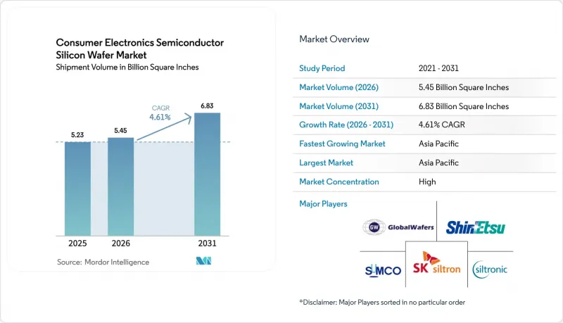
預計消費電子產品中使用的半導體矽晶圓市場規模將從 2025 年的 52.3 億平方英寸和 2026 年的 54.5 億平方英寸成長到 2031 年的 68.3 億平方英寸,2026 年至 2031 年的年複合成長率(CAGR)為 4.61%。
推動這一成長的主要因素包括對高度整合邏輯元件日益成長的需求、向先進製程節點的轉型以及政府主導的晶圓廠扶持措施。儘管大型晶圓代工廠仍專注於300毫米基板以實現晶片數量最大化,但諸如絕緣體上矽(SOI)等特種晶圓正不斷擴大市場佔有率,因為它們能夠提高5G智慧型手機的射頻效率。同時,由於模擬和分立元件仍採用成熟的製程節點,老一代200毫米晶圓產能的利潤率持續承壓。儘管美國和歐洲正在推進地域多角化,但亞太地區在成本、現有供應鏈和晶圓產能方面仍保持著結構性優勢。
全球消費性電子產品半導體矽晶圓市場趨勢及洞察。
5G相容智慧型手機的普及
行動電話廠商正在整合多個6GHz以下和毫米波前端模組,每個模組都包含用於低雜訊和功率放大器的獨立晶片。高通驍龍8 Elite採用先進的4nm製程製造,與先前的LTE平台相比,每個設備的晶圓面積增加了約30%。中國和印度正在部署獨立組網(SA)5G網路,即使全球出貨量趨於平穩,晶圓需求依然強勁。高頻SOI基板可降低訊號損耗,從而實現溢價,並支撐SOI晶圓5.31%的複合年成長率。氮化鎵和磷化銦放大器的部分替代正在推進,但這只會減緩矽需求的成長,而不會阻礙其成長。
高容量行動儲存(3D NAND)的成長
512GB 和 1TB 大容量智慧型手機的出現加速了向 232 層 NAND 快閃記憶體堆疊的過渡,導致晶圓開工量和返工週期增加。預計 2025 年下半年將供不應求促使 1Tb 晶片技術提前應用,增加了每Terabyte出貨量的矽消耗量。同時,三星和 SK 海力士將其 300mm 生產線改造為高容量記憶體生產線,進一步收緊了消費級 NAND 快閃記憶體的供應,並推高了晶圓的平均售價。隨著良率學習曲線的成熟和新產能的投入運作,由此帶來的需求激增將在兩年內達到高峰。
資本密集型大直徑晶體生長
包括拉拔機、切割鋸和測量儀器在內,一條300毫米柴可拉斯基法線的成本可能超過4億美元。設備前置作業時間通常超過兩年,導致經濟週期上行期新產能的推出延遲。 Siltronic公司預測2026年銷售額將出現中等個位數的下滑,這凸顯了庫存管理週期延長和資本投資延遲如何加重了固定成本的負擔。 SUMCO公司計劃在2026年底前關閉其位於宮崎的200毫米軋機工廠,這反映了現有產能過剩以及設備升級帶來的資本負擔。北美和歐洲人事費用和能源成本的上漲進一步提高了損益平衡點,加劇了這些限制因素。
細分市場分析
到2025年,300毫米晶圓將佔據消費性電子半導體矽晶圓市場71.29%的佔有率。這反映出其在每片晶圓晶片數量方面具有更優的經濟效益,足以抵消較高的設備成本。隨著晶圓代工廠在3奈米和環柵(GaAA)工藝節點上進行創紀錄的資本投資,該細分市場正以4.61%的複合年成長率與整體市場保持一致。光是台積電就已在其2026年的擴張計畫中累計520億至560億美元,幾乎全部用於300毫米晶圓廠。預計到2031年,300毫米平台的消費性電子半導體矽晶圓市場規模將達到49億平方英吋。
新興的減薄和鍵合技術使得厚度小於50µm的300mm基板成為可能,從而拓展了先前僅限於小直徑基板的應用領域。同時,在類比、MEMS和功率分離式元件領域,200mm生產線仍佔據主導地位,因為製程轉型帶來的效益有限。小於150mm的晶圓主要轉向高電阻射頻開關和特殊感測器等小眾應用。供應鏈的精簡,包括SUMCO宮崎工廠的關閉,有助於穩定傳統節點的價格,即便高階300mm晶圓的產量正在成長。
《消費性電子設備半導體矽晶圓市場報告》以晶圓直徑(150毫米及以下、200毫米、300毫米)、半導體裝置類型(邏輯裝置、記憶體等)、晶圓類型(優質拋光晶圓、外延晶圓、特種矽晶圓等)及地區(北美、歐洲、亞太地區進行細分、中東、歐洲和非洲)和地區(北美、歐洲、亞太非洲)。市場預測以出貨量(平方英吋)為單位。
區域分析
亞太地區預計到2025年將佔全球出貨量的84.78%,繼續保持其在消費電子半導體矽晶圓市場的領先地位,並預計到2031年將以5.78%的複合年成長率成長。該地區受益於台灣、韓國、日本和中國強大的供應鏈,每個地區都獲得了數十億美元的獎勵,用於建造先進的邏輯晶圓廠。台積電2026年的大規模資本投資計畫以及中國力爭佔據全球整體四分之一12吋晶圓產能的目標,進一步支撐了市場需求。韓國企業正在將其300毫米生產線改造為高容量記憶體生產線,導致通用NAND快閃記憶體的本地供應趨緊。印度100億美元的半導體發展計畫帶來了新的提案,但該國的晶圓生產仍嚴重依賴進口。
在北美,《晶片與科學法案》已向晶圓廠建設注入了364億美元,推動了低基數下的成長。台積電位於亞利桑那州的工廠和英特爾位於俄亥俄州的計畫預計將在2027年量產後刺激當地晶圓需求。 GlobalWafers計劃在美國建造其20年來的首座300毫米晶圓廠,但不斷上漲的人事費用和電力成本正在削弱其成本競爭力。在歐洲,歐盟《晶片與科學法案》已調動了800億歐元資金,專注於德國和法國的類比和功率裝置。 Siltronic的銷售前景顯示庫存將持續下降,但區域投資可望減緩人才流失到亞洲的趨勢。
即使將南美洲、中東和非洲這三個地區加起來,它們在消費性電子產品用半導體矽晶圓的市場佔有率也僅佔很小一部分。這是因為這些地區缺乏大規模的晶體生長設施。這些地區依賴從亞洲進口,也從歐洲和美國進口一些。雖然ISO 9001和ISO 14001等國際標準保證了產品品質的一致性,但地理集中使得供應鏈仍然容易受到自然災害和地緣政治緊張局勢的影響。
其他好處:
- Excel格式的市場預測(ME)表
- 3個月的分析師支持
目錄
第1章:引言
- 研究假設和市場定義
- 調查範圍
第2章:調查方法
第3章執行摘要
第4章 市場狀況
- 市場概覽
- 市場促進因素
- 5G相容智慧型手機的普及
- 高容量行動儲存(3D NAND)的成長
- 消費性物聯網和穿戴式裝置的擴展
- 政府對國內邏輯元件製造的獎勵
- TSV 中介層在 AR/ VR頭戴裝置的應用
- 矽光電在XR裝置的應用
- 市場限制因素
- 資本密集型大直徑晶體生長
- 高純度多晶矽的供應限制
- 射頻模組向複合基板的過渡
- 消費者OEM製造商設定碳足跡限制
- 產業價值鏈分析
- 監理情勢
- 技術分析
- 宏觀經濟因素對市場的影響
- 波特五力分析
- 供應商的議價能力
- 買方的議價能力
- 新進入者的威脅
- 替代品的威脅
- 競爭公司之間的競爭
第5章 市場規模與成長預測
- 依晶圓直徑
- 最大可達 150 毫米
- 200 mm
- 300 mm
- 依半導體裝置類型
- 邏輯
- 記憶
- 模擬
- 離散的
- 其他半導體裝置(光電子裝置、感測器、微型元件)
- 依晶片類型
- 拋光
- 外延
- 絕緣體上矽(SOI)
- 特種矽(高電阻、高功率、感測器級)
- 按地區
- 北美洲
- 美國
- 加拿大
- 墨西哥
- 歐洲
- 德國
- 英國
- 法國
- 其他歐洲地區
- 亞太地區
- 中國
- 日本
- 印度
- 韓國
- 台灣
- 亞太其他地區
- 南美洲
- 中東
- 非洲
- 北美洲
第6章 競爭情勢
- 市場集中度
- 策略趨勢
- 市佔率分析
- 公司簡介
- Shin-Etsu Chemical Co., Ltd.
- SUMCO Corporation
- GlobalWafers Co., Ltd.
- Siltronic AG
- SK siltron Co., Ltd.
- Soitec SA
- National Silicon Industry Group Co., Ltd.
- Wafer Works Corp.
- Okmetic Oy
- Ferrotec Holdings Corporation
- Hebei Puxing Electronic Technology Co., Ltd.
- Zhonghuan Semiconductor Co., Ltd.
- Hangzhou Semiconductor Wafer Co., Ltd.
- GRINM Semiconductor Materials Co., Ltd.
- MCL Electronic Materials Co., Ltd.
- Shanghai Simgui Technology Co., Ltd.
- Virginia Semiconductor, Inc.
- Silicon Valley Microelectronics, Inc.
- Topsil Semiconductor Materials A/S
- Silicon Materials, Inc.
第7章 市場機會與未來展望
The Consumer Electronics Semiconductor Silicon Wafer Market size in terms of shipment volume is projected to expand from 5.23 Billion Square Inches in 2025 and 5.45 Billion Square Inches in 2026 to 6.83 Billion Square Inches by 2031, registering a CAGR of 4.61% between 2026 to 2031.
Strengthening demand for logic-intensive devices, migration to advanced node geometries, and government-backed fab incentives anchor this growth. Capital outlays by leading foundries continue to favor 300 mm substrates that maximize die counts, while specialty wafers such as silicon-on-insulator (SOI) gain share because they enable higher radio-frequency efficiency in 5G smartphones. Conversely, trailing-edge 200 mm capacity faces enduring margin pressure as analog and discrete devices remain on mature nodes. Regional diversification efforts in the United States and Europe are underway, yet Asia-Pacific retains its structural advantage in cost, existing supply chains, and installed wafer capacity.
Global Consumer Electronics Semiconductor Silicon Wafer Market Trends and Insights
Proliferation of 5G-Enabled Smartphones
Handset vendors embed multiple sub-6 GHz and millimeter-wave front-end modules, each containing discrete dies for low-noise and power amplifiers. Qualcomm's Snapdragon 8 Elite, fabricated on an advanced 4 nm process, allocates roughly 30% more wafer area per device than previous LTE platforms. Stand-alone 5G networks are rolling out in China and India, sustaining wafer pull-through even as global unit shipments plateau. Radio-frequency SOI substrates mitigate signal loss, enabling premium pricing that supports the 5.31% CAGR for SOI wafers. Partial substitution by gallium-nitride and indium-phosphide amplifiers tempers, but does not derail, incremental silicon demand.
Growth in High-Capacity Mobile Storage (3D NAND)
Smartphones equipped with 512 GB and 1 TB tiers accelerated a shift to 232-layer NAND stacks, increasing wafer starts and rework cycles. Reported shortages in late 2025 drove an earlier adoption of 1 Tb die schemes, raising silicon consumption per terabyte shipped. Concurrently, Samsung and SK hynix redirected 300 mm lines toward high-bandwidth memory, constricting consumer-grade NAND supply and lifting wafer average selling prices. The resulting demand spike peaks within two years as yield learning curves mature and new capacity comes online.
Capital-Intensive Large-Diameter Crystal Growth
A single 300 mm Czochralski line can exceed USD 400 million when factoring in pullers, slicing saws, and metrology. Equipment lead times often surpass two years, delaying new capacity during cyclical upswings. Siltronic's mid-single-digit revenue decline outlook for 2026 underscores how prolonged inventory digestion and deferred capex amplify fixed-cost exposure. SUMCO's planned closure of its Miyazaki 200 mm plant by the end of 2026 reflects legacy overcapacity and the capital burden of retooling. Higher labor and energy costs in North America and Europe further elevate breakeven thresholds, tightening this restraint.
Other drivers and restraints analyzed in the detailed report include:
- Expansion of Consumer IoT and Wearables
- Government Incentives for Domestic Logic Fabs
- Carbon-Footprint Caps from Consumer OEMs
For complete list of drivers and restraints, kindly check the Table Of Contents.
Segment Analysis
The 300 mm class captured 71.29% of the consumer electronics semiconductor silicon wafer market share in 2025, reflecting superior die-per-wafer economics that outweigh higher tool costs. This segment follows a growth curve aligned with the overall 4.61% CAGR as foundries channel record capex toward 3 nm and gate-all-around nodes. TSMC alone earmarked USD 52-56 billion for 2026 expansions, nearly all of which were devoted to 300 mm fabs. The consumer electronics semiconductor silicon wafer market size for 300 mm platforms is poised to reach 4,900 million square inches by 2031.
Emerging thinning and bonding techniques enable 300 mm substrates below 50 µm, unlocking applications once restricted to smaller diameters. Meanwhile, 200 mm lines persist for analog, MEMS, and power discretes, where process migration delivers limited benefit. Sub-150-mm wafers are receding to niche roles, chiefly high-resistivity RF switches and specialty sensors. Supply rationalization, including SUMCO's Miyazaki shutdown, helps stabilize pricing for legacy nodes even as premium 300 mm output scales.
The Consumer Electronics Semiconductor Silicon Wafer Market Report is Segmented by Wafer Diameter (Up To 150 Mm, 200 Mm, 300 Mm), Semiconductor Device Type (Logic, Memory, and More), Wafer Type (Prime Polished, Epitaxial, Specialty Silicon, and More), and Geography (North America, Europe, Asia-Pacific, South America, Middle East, Africa). The Market Forecasts are Provided in Terms of Shipment Volume (Square Inches).
Geography Analysis
Asia-Pacific led the consumer electronics semiconductor silicon wafer market share with 84.78% of 2025 volume and is advancing at a 5.78% CAGR through 2031. The region benefits from deep supply chains in Taiwan, South Korea, Japan, and China, each supported by multi-billion-dollar incentives for advanced logic fabs. TSMC's heavy 2026 capital program and China's goal of holding one-quarter of global 12-inch capacity further anchor demand. South Korean firms are pivoting 300 mm lines to high-bandwidth memory, tightening local supply for commodity NAND. India's USD 10 billion semiconductor mission brings new proposals, yet wafer production there still relies on imports.
North America is growing from a low base as the CHIPS and Science Act channels USD 36.4 billion into fab construction. TSMC's Arizona complex and Intel's Ohio project will stimulate local substrate pull once high-volume manufacturing begins in 2027. GlobalWafers plans the first U.S. 300 mm wafer plant in two decades, but higher labor and power costs temper its cost position. Europe mobilized EUR 80 billion under the EU Chips Act, focusing on analog and power devices in Germany and France. Siltronic's revenue outlook points to continued inventory digestion, yet regional funding should slow the talent drain to Asia.
South America, the Middle East, and Africa together account for only a sliver of the consumer electronics semiconductor silicon wafer market size because they lack large crystal-growth facilities. These regions depend on imports from Asia and, to a lesser extent, Europe and the United States. Global ISO 9001 and ISO 14001 standards maintain product quality consistency, but geographic concentration still exposes the supply chain to natural disasters and geopolitical tensions.
- Shin-Etsu Chemical Co., Ltd.
- SUMCO Corporation
- GlobalWafers Co., Ltd.
- Siltronic AG
- SK siltron Co., Ltd.
- Soitec S.A.
- National Silicon Industry Group Co., Ltd.
- Wafer Works Corp.
- Okmetic Oy
- Ferrotec Holdings Corporation
- Hebei Puxing Electronic Technology Co., Ltd.
- Zhonghuan Semiconductor Co., Ltd.
- Hangzhou Semiconductor Wafer Co., Ltd.
- GRINM Semiconductor Materials Co., Ltd.
- MCL Electronic Materials Co., Ltd.
- Shanghai Simgui Technology Co., Ltd.
- Virginia Semiconductor, Inc.
- Silicon Valley Microelectronics, Inc.
- Topsil Semiconductor Materials A/S
- Silicon Materials, Inc.
Additional Benefits:
- The market estimate (ME) sheet in Excel format
- 3 months of analyst support
TABLE OF CONTENTS
1 INTRODUCTION
- 1.1 Study Assumptions and Market Definition
- 1.2 Scope of the Study
2 RESEARCH METHODOLOGY
3 EXECUTIVE SUMMARY
4 MARKET LANDSCAPE
- 4.1 Market Overview
- 4.2 Market Drivers
- 4.2.1 Proliferation of 5G-Enabled Smartphones
- 4.2.2 Growth in High-Capacity Mobile Storage (3D NAND)
- 4.2.3 Expansion of Consumer IoT and Wearables
- 4.2.4 Government Incentives for Domestic Logic Fabs
- 4.2.5 Adoption of TSV Interposers in AR/VR Headsets
- 4.2.6 Silicon Photonics Uptake in XR Devices
- 4.3 Market Restraints
- 4.3.1 Capital-Intensive Large-Diameter Crystal Growth
- 4.3.2 Supply Constraints of High-Purity Polysilicon
- 4.3.3 Shift of RF Modules to Compound Substrates
- 4.3.4 Carbon-Footprint Caps from Consumer OEMs
- 4.4 Industry Value Chain Analysis
- 4.5 Regulatory Landscape
- 4.6 Technology Analysis
- 4.7 Impact of Macroeconomic Factors on the Market
- 4.8 Porter's Five Forces Analysis
- 4.8.1 Bargaining Power of Suppliers
- 4.8.2 Bargaining Power of Buyers
- 4.8.3 Threat of New Entrants
- 4.8.4 Threat of Substitutes
- 4.8.5 Intensity of Competitive Rivalry
5 MARKET SIZE AND GROWTH FORECASTS (VOLUME)
- 5.1 By Wafer Diameter
- 5.1.1 Up to 150 mm
- 5.1.2 200 mm
- 5.1.3 300 mm
- 5.2 By Semiconductor Device Type
- 5.2.1 Logic
- 5.2.2 Memory
- 5.2.3 Analog
- 5.2.4 Discrete
- 5.2.5 Other Semiconductor Device Types (Optoelectronics, Sensors, Micro)
- 5.3 By Wafer Type
- 5.3.1 Prime Polished
- 5.3.2 Epitaxial
- 5.3.3 Silicon-on-Insulator (SOI)
- 5.3.4 Specialty Silicon (High-Resistivity, Power, Sensor-Grade)
- 5.4 By Geography
- 5.4.1 North America
- 5.4.1.1 United States
- 5.4.1.2 Canada
- 5.4.1.3 Mexico
- 5.4.2 Europe
- 5.4.2.1 Germany
- 5.4.2.2 United Kingdom
- 5.4.2.3 France
- 5.4.2.4 Rest of Europe
- 5.4.3 Asia-Pacific
- 5.4.3.1 China
- 5.4.3.2 Japan
- 5.4.3.3 India
- 5.4.3.4 South Korea
- 5.4.3.5 Taiwan
- 5.4.3.6 Rest of Asia-Pacific
- 5.4.4 South America
- 5.4.5 Middle East
- 5.4.6 Africa
- 5.4.1 North America
6 COMPETITIVE LANDSCAPE
- 6.1 Market Concentration
- 6.2 Strategic Moves
- 6.3 Market Share Analysis
- 6.4 Company Profiles (includes Global Level Overview, Market Level Overview, Core Segments, Financials as available, Strategic Information, Market Rank/Share, Products and Services, Recent Developments)
- 6.4.1 Shin-Etsu Chemical Co., Ltd.
- 6.4.2 SUMCO Corporation
- 6.4.3 GlobalWafers Co., Ltd.
- 6.4.4 Siltronic AG
- 6.4.5 SK siltron Co., Ltd.
- 6.4.6 Soitec S.A.
- 6.4.7 National Silicon Industry Group Co., Ltd.
- 6.4.8 Wafer Works Corp.
- 6.4.9 Okmetic Oy
- 6.4.10 Ferrotec Holdings Corporation
- 6.4.11 Hebei Puxing Electronic Technology Co., Ltd.
- 6.4.12 Zhonghuan Semiconductor Co., Ltd.
- 6.4.13 Hangzhou Semiconductor Wafer Co., Ltd.
- 6.4.14 GRINM Semiconductor Materials Co., Ltd.
- 6.4.15 MCL Electronic Materials Co., Ltd.
- 6.4.16 Shanghai Simgui Technology Co., Ltd.
- 6.4.17 Virginia Semiconductor, Inc.
- 6.4.18 Silicon Valley Microelectronics, Inc.
- 6.4.19 Topsil Semiconductor Materials A/S
- 6.4.20 Silicon Materials, Inc.
7 MARKET OPPORTUNITIES AND FUTURE OUTLOOK
- 7.1 White-Space and Unmet-Need Assessment
 釹、鐵、硼磁體市場規模、佔有率、趨勢及預測:按應用和地區分類,2026-2034年磁鐵市場報告:按磁鐵類型、應用和國家分類(2026-2034 年)釤鈷磁鐵市場報告:按應用和地區分類(2026-2034 年)
 2026年全球醫用磁鐵市場報告
 全球釤鈷磁鐵市場:策略性洞察與預測(2026-2031年)
 弧形鐵氧體磁體市場規模、佔有率和成長分析:按磁鐵類型、應用領域、形狀、終端用戶產業和地區分類-2026-2033年產業預測
 磁鐵市場分析及預測(至2035年):類型、產品類型、應用、材質類型、技術、最終用戶、組件、功能、形狀、安裝類型全球釤鈷磁鐵市場規模、佔有率、趨勢和成長分析報告(2026-2034年)日本磁鐵市場報告:磁鐵類型、應用及地區(2026-2034年)2026年全球電子磁鐵市場報告