


 |
市場調查報告書
商品編碼
2044005
汽車半導體矽晶圓:市場佔有率分析、產業趨勢與統計及成長預測(2026-2031)Automotive Semiconductor Silicon Wafer - Market Share Analysis, Industry Trends & Statistics, Growth Forecasts (2026 - 2031) |
||||||

※ 本網頁內容可能與最新版本有所差異。詳細情況請與我們聯繫。
預計汽車半導體矽晶圓的市場規模將從 2025 年的 26.1 億平方英寸成長到 2026 年的 27.8 億平方英寸,到 2031 年達到 38.8 億平方英寸,2026 年至 2031 年的複合年成長率為 6.92%。
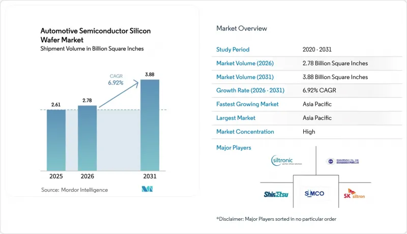
乘用車快速電氣化、向800V電池組的過渡以及軟體定義車輛計算領域的興起是推動這一成長的主要因素。儘管優質拋光矽的出貨量仍然最大,但200mm基板上的寬能隙碳化矽外延晶圓仍佔了成長的大部分佔有率。美國、歐洲、韓國和印度的政策獎勵正在縮短晶圓廠的投資回收期,但持續的基板短缺和較長的車規級認證週期限制了短期產量。垂直整合和向300mm基板的過渡等競爭措施正在重塑成本曲線,這將決定汽車半導體矽晶圓市場的未來方向。
全球汽車半導體矽晶圓市場趨勢及洞察
電動車的廣泛普及以及向800V車輛平台的過渡
配備 800V 電池組的電動車車型需要額定電壓為 1200V 的 SiC MOSFET,而這又需要基面位錯密度極低的 200mm 外延晶圓。繼現代 Ioniq 5 和起亞 EV6 等新車型上市後,保時捷、奧迪和通用汽車也正在為其 2026 年車型製定類似的藍圖。英飛凌 Klim 工廠產能的提升以及意法半導體簽訂的長期晶圓供應契約,凸顯了在產量成長之前確保材料供應的激烈競爭。這種結構性需求導致前置作業時間超過 12 個月,凸顯了穩定基板供應的緊迫性。
800V充電基礎設施快速發展
預計到2025年,公共和私人對超快充電的投資將超過120億美元。歐洲AFIR法規要求到2027年,主要高速公路沿線每60公里安裝一個400kW的充電樁。由於每個800V汽車充電樁都包含6到8個SiC MOSFET,這些MOSFET形成於150mm至200mm的晶圓上,因此加速充電樁部署將直接導致晶圓需求增加。中國目前已佔全球800V充電站總數的60%以上,鞏固了在亞太地區的領先地位。 Soytech的Power-SOI基板在PCB面積有限的閘極驅動器插座市場正日益受到重視。由於車載電路板(OBC)的設計週期比基礎建設落後約18個月,預計2027年至2028年間將有顯著的需求成長。
200mm基板供不應求
2025年全球200毫米碳化矽晶圓產能僅120萬片,但預計2028年汽車產業的需求將超過200萬片。每個PVT反應器的成本可高達800萬美元,認證需要18至24個月,因此供應狀況的顯著改善預計較為緩慢。儘管Wolfspeed位於Cylar City的工廠擴建工程將持續到2027年,但歐洲和北美的OEM廠商仍嚴重依賴從亞洲進口。這種供不應求迫使廠商採取雙重採購策略,並延長設計週期,短期內將使該產業的複合年成長率下降1.2個百分點。
細分市場分析
到2025年,200mm晶圓將佔據汽車半導體矽晶圓市場56.48%的佔有率,並將繼續成為SiC功率分離式元件、閘極驅動器和電源管理積體電路(PMIC)的關鍵元件。折舊免稅額且已折舊的製程節點仍保持著可觀的營運利潤率,且牽引MOSFET的晶片尺寸與200mm晶圓的經濟性完美契合。然而,隨著德州儀器、台積電和GlobalWafers等公司將MCU和混合訊號IC轉移到更大的晶圓上,300mm晶圓的產能正以7.45%的複合年成長率成長,單晶片成本降低了20%以上。 Wolfspeed的300mm SiC樣品實現了低於1cm²的缺陷密度,證明了其技術可行性,並為2028年後功率裝置的大規模供應鋪平了道路。
汽車半導體矽晶圓市場預計將呈現兩極化的模式。一旦認證障礙消除,300mm晶圓有望主導運算和混合訊號領域,而200mm晶圓在SiC領域可能仍將繼續使用,直到晶體生長技術跟上步伐。隨著舊晶圓廠的逐步淘汰,150mm以下尺寸的晶圓尺寸持續縮小,但閘流體和客製化類比裝置的需求仍然存在。 Soytech正將其Power-SOI產品升級至300mm尺寸,以滿足電池管理的需求,這凸顯了電氣化專案中對更嚴格成本結構的必要性。
《汽車半導體矽晶圓市場報告》依晶圓直徑(150毫米及以下、200毫米、300毫米)、半導體裝置類型(邏輯元件、記憶體、類比元件、分立元件及其他)、晶圓類型(拋光面、外延面、SOI、特種矽)和地區細分(北美、歐洲、亞太、南美、非洲地區)和地區進行細分(北美、歐洲、亞太地區)和地區進行細分、歐洲和亞太地區。市場預測以體積(平方英吋)為單位。
區域分析
預計到2025年,亞太地區將佔據汽車半導體矽晶圓市場84.19%的佔有率,複合年成長率(CAGR)為7.59%。台灣地區在6奈米以下製程的產能方面佔據顯著佔有率,並且在成熟節點汽車晶圓的初創企業中佔比超過40%。同時,中國正在推進碳化矽晶體生長、外延和裝置製造工廠的整合。韓國斥資700兆韓元(約5,250億美元)的策略正在透過新增10條化合物半導體生產線來鞏固該地區的基礎。日本基板巨頭,如信越化學和SUMCO,在300毫米優質拋光晶圓和碳化矽外延晶圓的供應方面處於領先地位。印度政府支持的12吋生產線預計到2026年將達到每月5萬片晶圓的產能。
2025年北美地區的晶片出貨量小規模,但「晶片法案」(CHIPS Act)的獎勵已資助GlobalWafers的300毫米晶圓廠和Wolfspeed的碳化矽(SiC)巨型晶圓廠的建設,預計到2028年,這兩家工廠每年將額外生產100萬公片的2000毫米微晶片。然而,儘管大力推進本地化,許多模組仍然依賴亞洲製造的基板,即便美國輕型汽車年產量已超過1500萬輛。歐洲佔了相當大的市場佔有率,並受益於IPCEI-ME/CT的資金支持,用於擴大英飛凌、意法半導體和Webers等公司在全球範圍內的產能,但其超過70%的優質拋光晶圓需求仍然依賴進口。
除了南美洲,中東和非洲也由於生態系統深度有限和資金壁壘,產能仍然較低。為了降低供應鏈風險,汽車製造商目前正在聯合認證來自多個地區的供應商,但汽車級合金18-24個月的生產週期意味著,實質的多元化預計將推遲到2027年下半年。始於2024年下半年的庫存調整似乎已在2026年初觸底,晶圓訂單在新簽訂的長期供應合約下也顯示出復甦跡象。
其他好處
- Excel格式的市場預測(ME)表
- 3個月的分析師支持
目錄
第1章:引言
- 研究假設和市場定義
- 調查範圍
第2章:調查方法
第3章執行摘要
第4章 市場狀況
- 市場概覽
- 產業價值鏈分析
- 技術分析
- 宏觀經濟因素對市場的影響
- 波特五力分析
- 供應商的議價能力
- 買方的議價能力
- 新進入者的威脅
- 替代品的威脅
- 競爭公司之間的競爭
- 市場促進因素
- 電動車的廣泛普及以及向800V車輛平台的過渡
- 800V充電基礎設施快速發展
- 在高溫和高頻性能方面優於矽
- 政府對寬能隙裝置製造的支援措施
- 中國碳化矽垂直整合供應鏈的興起
- 200mm 塊體生長技術新突破,降低缺陷密度
- 市場限制因素
- 200mm基板供不應求
- 包裝引起的熱機械應力
- 資本密集型晶體生長裝置
- 碳化矽切削屑回收利用面臨的挑戰
第5章 市場規模與成長預測
- 依晶圓直徑
- 150毫米或更小
- 200mm
- 300mm
- 依半導體裝置類型
- 邏輯
- 記憶
- 模擬
- 離散的
- 其他半導體裝置類型
- 依晶片類型
- 拋光
- 外延
- 絕緣體上矽(SOI)
- 特種矽(高電阻、高功率、感測器級)
- 按地區
- 北美洲
- 美國
- 加拿大
- 墨西哥
- 歐洲
- 德國
- 英國
- 法國
- 其他歐洲國家
- 亞太地區
- 中國
- 日本
- 印度
- 韓國
- 台灣
- 亞太其他地區
- 南美洲
- 中東和非洲
- 北美洲
第6章 競爭情勢
- 市場集中度
- 策略趨勢
- 市佔率分析
- 公司簡介
- Shin-Etsu Chemical Co., Ltd.
- SUMCO Corporation
- Siltronic AG
- GlobalWafers Co., Ltd.
- SK Siltron Co., Ltd.
- Soitec SA
- Okmetic Oy
- Wafer Works Corp.
- Topsil Semiconductor Materials A/S
- Shanghai Simgui Technology Co., Ltd.
- MEMC Electronic Materials, Inc.
- Infineon Technologies AG
- ON Semiconductor Corp.
- STMicroelectronics NV
- NXP Semiconductors NV
- Renesas Electronics Corp.
- Texas Instruments Inc.
- X-FAB Silicon Foundries SE
- Wolfspeed, Inc.
第7章 市場機會與未來展望
The automotive semiconductor silicon wafer market size is expected to increase from 2.61 Billion Square Inches in 2025 to 2.78 billion Square Inches in 2026 and reach 3.88 Billion Square Inches by 2031, growing at a CAGR of 6.92% over 2026-2031.
The expansion is powered by the rapid electrification of passenger vehicles, the migration to 800-volt battery packs, and the rise of software-defined vehicle compute domains. Wide-bandgap SiC epitaxial wafers on 200 mm substrates are absorbing much of the incremental volume, even as prime-polished silicon continues to ship the most pieces. Policy incentives in the United States, Europe, South Korea, and India are shortening fab paybacks, while ongoing substrate shortages and long automotive-grade qualification cycles moderate near-term output. Competitive moves toward vertical integration and 300 mm migration are reshaping cost curves and will decide the future trajectory of the automotive semiconductor silicon wafer market.
Global Automotive Semiconductor Silicon Wafer Market Trends and Insights
Rising EV Penetration And Shift Toward 800V Vehicle Platforms
Electric models built on 800-volt packs need SiC MOSFETs rated at 1,200 V, which in turn require 200 mm epitaxial wafers with extremely low basal-plane dislocation densities. Launches such as Hyundai's Ioniq 5 and Kia's EV6 have triggered similar roadmaps from Porsche, Audi, and General Motors for model-year 2026 designs. Capacity additions at Infineon's Kulim facility and long-term wafer supply agreements signed by STMicroelectronics underscore the race to lock in material ahead of volume hikes. The structural pull tightens lead times beyond 12 months and underscores the importance of secure substrate access.
Rapid Build-Out Of 800V Charging Infrastructure
Public and private spending on ultra-fast charging surpassed USD 12 billion in 2025, and Europe's AFIR rule mandates 400 kW chargers every 60 km on core corridors by 2027. Each 800 V on-board charger integrates six to eight SiC MOSFETs grown on 150 mm- to 200-mm wafers, so faster charger rollouts translate directly into increased wafer demand. Chinese deployments already account for more than 60% of global 800 V posts, reinforcing Asia-Pacific's dominance. Soitec's Power-SOI substrates are winning gate-driver sockets where PCB area is tight. Because OBC design cycles lag infrastructure by roughly 18 months, the full volume effect will surface between 2027 and 2028.
Limited Availability Of 200 mm Substrates
Global capacity reached only 1.2 million 200 mm SiC wafers in 2025, yet automotive demand will surpass 2 million units before 2028. Each PVT reactor costs up to USD 8 million and needs 18-24 months to qualify, delaying meaningful relief. Wolfspeed's Siler City expansion runs through 2027, while European and North American OEMs still rely heavily on Asian imports. The shortage forces dual-sourcing and stretches design cycles, trimming 1.2 percentage points off the sector CAGR in the near term.
Other drivers and restraints analyzed in the detailed report include:
- High-Temperature, High-Frequency Performance Advantages Over Si
- Government Incentives For Wide-Band-Gap Fabs
- Packaging-Induced Thermo-Mechanical Stress
For complete list of drivers and restraints, kindly check the Table Of Contents.
Segment Analysis
The 200 mm tranche held 56.48% automotive semiconductor silicon wafer market share in 2025 and remains indispensable for SiC power discretes, gate drivers, and PMICs. Mature-node lines already depreciated keep operating margins attractive, and the die sizes of traction MOSFETs fit 200 mm economics well. However, 300 mm capacity is climbing at a 7.45% CAGR because Texas Instruments, TSMC, and GlobalWafers are shifting MCUs and mixed-signal ICs onto larger wafers, driving 20%-plus cost reductions per die. Wolfspeed's 300 mm SiC samples delivered sub-1 cm-2 defect densities, proving technical feasibility and pointing toward high-volume power-device supply after 2028.
The automotive semiconductor silicon wafer market is likely to bifurcate, 300 mm will dominate compute and mixed-signal content once qualification barriers fall, while 200 mm persists in SiC until crystal growth catches up. Up-to-150 mm formats continue sliding as legacy fabs retire, although they retain pockets of demand for thyristors and custom analog. Soitec is migrating Power-SOI to 300 mm to meet demand for battery management, highlighting the need for tighter cost structures in electrification programs.
The Automotive Semiconductor Silicon Wafer Market Report is Segmented by Wafer Diameter (Up To 150 Mm, 200 Mm, and 300 Mm), Semiconductor Device Type (Logic, Memory, Analog, Discrete, and Other Types), Wafer Type (Prime Polished, Epitaxial, SOI, and Specialty Silicon), and Geography (North America, Europe, Asia-Pacific, South America, Middle East and Africa). The Market Forecasts are Provided in Terms of Volume (Square Inches).
Geography Analysis
Asia-Pacific held 84.19% automotive semiconductor silicon wafer market share in 2025 and is expanding at 7.59% CAGR. Taiwan accounts for a considerable share of sub-6 nm capacity and more than 40% of mature-node automotive wafer starts, while China continues to integrate SiC crystal growth, epitaxy, and device fabs. South Korea's 700 trillion KRW (USD 525 billion) strategy adds 10 new facilities and compound-semiconductor lines, reinforcing regional depth. Japan's substrate majors, including Shin-Etsu and SUMCO, anchor 300 mm prime polished and SiC epitaxial supply, and India's state-backed 12-inch line will bring 50,000 wafers per month online in 2026.
North America controlled a small share of shipments in 2025, but CHIPS Act incentives fund GlobalWafers' 300 mm plant and Wolfspeed's SiC megafab, together adding more than one million 200 mm-equivalent wafers annually by 2028. The localization push, however, still leaves many modules reliant on Asian substrates, as U.S. light-vehicle output surpasses 15 million units yearly. Europe holds a considerable share and benefits from IPCEI-ME/CT funding for capacity at Infineon, STMicroelectronics, and GlobalWafers, yet imports cover over 70% of prime polished demand.
South America plus Middle East and Africa together remain low due to limited ecosystem depth and capital barriers. To mitigate supply-chain risk, automakers now co-qualify multiple geographic sources even though the 18-to-24-month automotive-grade cycle delays meaningful diversification until late 2027. Inventory corrections that began in late-2024 appear to have bottomed by early-2026, and wafer call-offs are rebounding under new long-term supply agreements.
- Shin-Etsu Chemical Co., Ltd.
- SUMCO Corporation
- Siltronic AG
- GlobalWafers Co., Ltd.
- SK Siltron Co., Ltd.
- Soitec S.A.
- Okmetic Oy
- Wafer Works Corp.
- Topsil Semiconductor Materials A/S
- Shanghai Simgui Technology Co., Ltd.
- MEMC Electronic Materials, Inc.
- Infineon Technologies AG
- ON Semiconductor Corp.
- STMicroelectronics N.V.
- NXP Semiconductors N.V.
- Renesas Electronics Corp.
- Texas Instruments Inc.
- X-FAB Silicon Foundries SE
- Wolfspeed, Inc.
Additional Benefits:
- The market estimate (ME) sheet in Excel format
- 3 months of analyst support
TABLE OF CONTENTS
1 INTRODUCTION
- 1.1 Study Assumptions and Market Definition
- 1.2 Scope of the Study
2 RESEARCH METHODOLOGY
3 EXECUTIVE SUMMARY
4 MARKET LANDSCAPE
- 4.1 Market Overview
- 4.2 Industry Value Chain Analysis
- 4.3 Technology Analysis
- 4.4 Impact of Macroeconomic Factors on the Market
- 4.5 Porter's Five Forces Analysis
- 4.5.1 Bargaining Power of Suppliers
- 4.5.2 Bargaining Power of Buyers
- 4.5.3 Threat of New Entrants
- 4.5.4 Threat of Substitutes
- 4.5.5 Intensity of Competitive Rivalry
- 4.6 Market Drivers
- 4.6.1 Rising EV Penetration and Shift Toward 800-V Vehicle Platforms
- 4.6.2 Rapid Build-Out of 800 V Charging Infrastructure
- 4.6.3 High-Temperature, High-Frequency Performance Advantages Over Si
- 4.6.4 Government Incentives for Wide-Band-Gap Fabs
- 4.6.5 Emergence of Vertically-Integrated SiC Supply Chains in China
- 4.6.6 Novel 200 mm Bulk-Growth Breakthroughs Lowering Defect Density
- 4.7 Market Restraints
- 4.7.1 Limited Availability of 200 mm Substrates
- 4.7.2 Packaging-Induced Thermo-Mechanical Stress
- 4.7.3 Capital-Intensive Crystal-Growth Equipment
- 4.7.4 Recycling Challenges for SiC Kerf Waste
5 MARKET SIZE AND GROWTH FORECASTS (VOLUME)
- 5.1 By Wafer Diameter
- 5.1.1 Up to 150 mm
- 5.1.2 200 mm
- 5.1.3 300 mm
- 5.2 By Semiconductor Device Type
- 5.2.1 Logic
- 5.2.2 Memory
- 5.2.3 Analog
- 5.2.4 Discrete
- 5.2.5 Other Semiconductor Device Types
- 5.3 By Wafer Type
- 5.3.1 Prime Polished
- 5.3.2 Epitaxial
- 5.3.3 Silicon-on-Insulator (SOI)
- 5.3.4 Specialty Silicon (High-Resistivity, Power, Sensor-Grade)
- 5.4 By Geography
- 5.4.1 North America
- 5.4.1.1 United States
- 5.4.1.2 Canada
- 5.4.1.3 Mexico
- 5.4.2 Europe
- 5.4.2.1 Germany
- 5.4.2.2 United Kingdom
- 5.4.2.3 France
- 5.4.2.4 Rest of Europe
- 5.4.3 Asia-Pacific
- 5.4.3.1 China
- 5.4.3.2 Japan
- 5.4.3.3 India
- 5.4.3.4 South Korea
- 5.4.3.5 Taiwan
- 5.4.3.6 Rest of Asia-Pacific
- 5.4.4 South America
- 5.4.5 Middle East and Africa
- 5.4.1 North America
6 COMPETITIVE LANDSCAPE
- 6.1 Market Concentration
- 6.2 Strategic Moves
- 6.3 Market Share Analysis
- 6.4 Company Profiles (includes Global Level Overview, Market Level Overview, Core Segments, Financials as available, Strategic Information, Market Rank/Share, Products and Services, Recent Developments)
- 6.4.1 Shin-Etsu Chemical Co., Ltd.
- 6.4.2 SUMCO Corporation
- 6.4.3 Siltronic AG
- 6.4.4 GlobalWafers Co., Ltd.
- 6.4.5 SK Siltron Co., Ltd.
- 6.4.6 Soitec S.A.
- 6.4.7 Okmetic Oy
- 6.4.8 Wafer Works Corp.
- 6.4.9 Topsil Semiconductor Materials A/S
- 6.4.10 Shanghai Simgui Technology Co., Ltd.
- 6.4.11 MEMC Electronic Materials, Inc.
- 6.4.12 Infineon Technologies AG
- 6.4.13 ON Semiconductor Corp.
- 6.4.14 STMicroelectronics N.V.
- 6.4.15 NXP Semiconductors N.V.
- 6.4.16 Renesas Electronics Corp.
- 6.4.17 Texas Instruments Inc.
- 6.4.18 X-FAB Silicon Foundries SE
- 6.4.19 Wolfspeed, Inc.
7 MARKET OPPORTUNITIES AND FUTURE OUTLOOK
- 7.1 White-Space and Unmet-Need Assessment

 汽車人工智慧半導體市場預測至2034年—全球分析(按半導體類型、車輛類型、人工智慧功能、銷售管道、應用、最終用戶和地區分類)汽車半導體市場預測至2034年:按組件、半導體材料、感測器類型、銷售管道、最終用戶、應用和地區分類的全球分析
 汽車半導體市場:2026-2032年全球市場預測(按產品類型、半導體材料、動力類型、應用、車輛類型和最終用戶分類)汽車功率半導體市場預測至2034年-全球分析(按元件類型、材料、車輛類型、驅動系統、電壓範圍、封裝類型、應用、銷售管道和地區分類)
 汽車半導體市場機會、成長要素、產業趨勢分析及2026-2035年預測。汽車半導體市場預測至2034年:按組件、車輛類型、應用和地區分類的全球分析
 2026-2034年全球汽車半導體市場規模、佔有率、趨勢和成長分析報告汽車功率半導體市場:策略性洞察與預測(2026-2031年)
 汽車半導體市場:按應用和地區分類
 汽車半導體市場分析及預測(至2035年):依類型、產品類型、技術、組件、應用、材質、裝置、最終使用者、功能及安裝類型分類