


 |
市場調查報告書
商品編碼
2043992
通訊半導體用矽晶圓:市場佔有率分析、產業趨勢和統計數據以及成長預測(2026-2031 年)Telecommunication Semiconductor Silicon Wafer - Market Share Analysis, Industry Trends & Statistics, Growth Forecasts (2026 - 2031) |
||||||
※ 本網頁內容可能與最新版本有所差異。詳細情況請與我們聯繫。
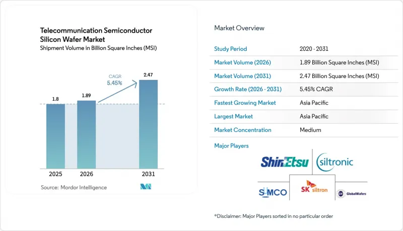
以出貨量為準,通訊半導體矽晶圓市場的市場規模預計將從 2025 年的 18 億平方英吋 (MSI) 成長到 2026 年的 18.9 億平方英吋 (MSI),並在 2031 年達到 24.7 億平方英吋 (MSI),2026 年至 2031 年的複合年成長率為 2031%。
產業向5G大規模MIMO基地台、早期6G研究平台和矽光電收發器的轉型,正在重新定義基板純度、直徑和缺陷密度的要求。政府支持的晶片類獎勵,尤其是在美國、歐盟、日本和韓國,正在刺激國內晶圓製造廠的建設,縮短先前集中在東亞的供應鏈。全球六大供應商之間的整合正在推進,鞏固了寡占的價格結構,而中國的新參與企業仍然受到14nm以下製造設備出口限制的限制。同時,更嚴格的廢棄物環境法規和不斷增加的資本密集度正在給成本結構帶來壓力,而通訊半導體矽晶圓市場正在向高附加價值特種基板轉變。
全球通訊半導體晶圓市場趨勢及洞察
5G/6G 基地台的快速部署需要高純度的 300mm 晶圓。
大規模MIMO基地台需要採用氮化鎵(GaN)功率放大器和矽射頻前端,這些元件需製造在電阻率超過1,000歐姆·公分的300毫米基板上,以降低3.5GHz以上頻段的基板損耗。 2025年全球矽晶圓出貨量將達到129.73億平方英寸,主要由通訊需求驅動。 Imec已成功檢驗了工作在7-24GHz頻段(專為6G設計)的GaN-on-SiIC射頻電晶體,這將使晶圓消耗量超出目前的5G需求。中國移動和中國電信計畫在2025年總合部署120萬個5G基地台,每個基地台大約需要200-300平方英吋的矽晶圓。目前只有兩家供應商能夠持續滿足毫米波應用所需的兆分之一(pptr)金屬污染閾值。
類似「CHIPS 法案」的政府獎勵正在加速通訊晶圓製造廠的擴張。
根據美國《晶片與科學法案》,到2025年,總計364億美元已分配給40個項目。其中,GlobalWafers公司獲得了4億美元,用於在德克薩斯州和密蘇裡州建造兩座300毫米晶圓製造廠。德州儀器公司獲得了16億美元,用於建造四座300毫米晶圓廠,以供應基地台回程傳輸和功率積體電路。歐洲根據《晶片與科學法案》出資430億歐元(約460億美元),以支持英飛凌和義法半導體公司射頻和功率晶圓的生產能力。儘管存在地緣政治摩擦,日本仍提供了9,200億美元(約62億美元)的補貼,以確保5G所需的300毫米基板供應。這些津貼將使實際資本成本降低25%至35%,並將投資回收期縮短至10年以內。
300毫米晶圓生產線是資本密集且投資回收期長的生產線。
新建一座300毫米晶圓廠的成本在30億至50億美元之間,其中資本投資高達70%。 Siltronic在新加坡的擴張計畫就充分體現了這項挑戰,該公司投資20億歐元(約21.4億美元)以確保年產100萬片晶圓的能力。即使是像SUMCO和SK Siltron這樣的老字型大小企業也成立了合資企業來分擔36億美元的建造成本。當補貼覆蓋的成本不足15%時,投資者將面臨10至15年的投資回收期,阻礙了新進者,並鞏固了寡占格局。
細分市場分析
預計到2025年,300mm晶圓的產量將佔總產量的64.48%,這得益於自動化帶來的優勢以及單晶片成本降低30-40%。 GlobalWafers位於謝爾曼的工廠於2025年交付了首批120萬片晶圓,印證了國內市場的強勁成長勢頭。德州儀器推出了四個模組,每個模組的月產能為4萬片晶圓,用於供應類比和嵌入式通訊積體電路。由於設備供不應求,200mm晶圓的產能仍緊張,因此需要對300mm生產線進行設計調整。小於150mm的晶圓仍是GaN功率射頻放大器和MEMS天線調諧器的小眾市場,但其市場佔有率持續萎縮。監管機構對晶圓直徑的選擇影響甚微,但對中國300mm晶圓製造設備的出口限制正在減緩該尺寸晶圓在中國的普及。
隨著晶片級架構的興起,每個無線前端都需要多個晶片,涵蓋電源、射頻和數位領域,這推動了對更大尺寸晶圓的需求。在通訊半導體矽晶圓市場,供應商為了確保銷量,將拋光後的晶圓和外延晶圓捆綁銷售。像SEMI這樣的行業組織正在製定缺口位置和厚度公差的標準化標準,使晶圓廠能夠快速認證多個供應商,這在一定程度上削弱了現有供應商的影響力,但仍然保持著新進入者較高的准入門檻。
《通訊半導體矽晶圓市場報告》依晶圓直徑(150毫米及以下、200毫米、300毫米)、半導體裝置類型(邏輯裝置、記憶體、模擬器及其他)、晶圓類型(拋光面、外延面、絕緣體上矽(SOI)及其他)及地區進行細分。市場預測以體積(平方英吋)為單位。
區域分析
預計到2025年,亞太地區將佔全球晶圓供應量的80.11%,並在2031年之前維持6.78%的複合年成長率。中國120萬個5G基地台的需求形成了壟斷性格局,國內供應商競相滿足此需求,但設備出口限制導致其良率低於日本水準。日本信越化學和SUMCO憑藉其在柴可拉斯基法無可比擬的專業技術,合計佔據了全球約55%的300毫米晶圓產能。韓國SUMCO和SK Siltron的合資企業計劃在2027年每年新增100萬片晶圓產能,其主要業務領域為通訊和汽車產業。台灣晶圓市場仍需求旺盛,主要得益於代工業的領軍企業台積電,其熊本工廠已獲得9,200億日圓(約62億美元)的政府補助。
北美地區正蓬勃發展,這得益於《晶片法案》(CHIPS Act)提供的364億美元資金。預計2027年,GlobalWafers和德州儀器(TI)將合計供應200萬片300毫米晶圓,進而降低對亞洲進口的依賴。在歐洲,《晶片法案》提供的430億歐元(約460億美元)資金正支持英飛凌(Infineon)和意法半導體(STMicroelectronics)的擴張,但不斷上漲的能源和人事費用使其市場佔有率保持在10%以下。南美、中東和非洲的規模仍然較小,主要依賴進口晶圓用於有限的5G部署。
美國、日本和荷蘭對14奈米以下製程設備的出口限制擾亂了亞太地區的供應鏈,迫使中國晶圓廠轉向28奈米製程,導致單功能晶圓面積增加高達60%。中國對鎵和鍺的報復性出口限制推高了化合物半導體的成本,迫使需求轉向日本和韓國的供應商,這些供應商已實現了原料來源多元化。由於新建晶圓廠的投資回收期需要10到15年,因此預計供應鏈多元化的努力要到2030年或更晚才能達到實質成果。
其他好處
- Excel格式的市場預測(ME)表
- 3個月的分析師支持
目錄
第1章:引言
- 研究假設和市場定義
- 調查範圍
第2章:調查方法
第3章執行摘要
第4章 市場狀況
- 市場概覽
- 產業價值鏈分析
- 監理情勢
- 技術分析
- 宏觀經濟因素對市場的影響
- 波特五力分析
- 供應商的議價能力
- 買方的議價能力
- 新進入者的威脅
- 替代品的威脅
- 競爭公司之間的競爭
- 市場促進因素
- 5G/6G 基地台部署的快速成長推高了對高純度 300mm 晶圓的需求。
- 類似於「晶片製造法」的政府獎勵正在加速晶圓製造廠的擴張,尤其是在通訊領域。
- 矽光電收發器的快速普及推高了對SOI晶圓的需求。
- 擴大300毫米雲端與邊緣資料流量處理器產能
- 對共封裝光學元件所需的超薄晶圓的需求正在推動新型拋光化學品的研發。
- 背面供電相容的晶圓,適用於配備人工智慧的基地台SoC
- 市場限制因素
- 300mm晶圓生產線面臨更高的資本密集度和更長的投資回收期。
- 高電阻射頻級晶圓的缺陷密度挑戰
- 關於先進晶圓製造設備出口的規定
- 對漿料廢棄物的更嚴格規定正在影響光電級 CMP 的成本。
第5章 市場規模與成長預測
- 依晶圓直徑
- 最大 150 毫米
- 200mm
- 300mm
- 依半導體裝置類型
- 邏輯
- 記憶
- 模擬
- 離散的
- 其他半導體裝置(光電子裝置、感測器、微型元件)
- 依晶片類型
- 拋光
- 外延
- 絕緣體上矽(SOI)
- 特種矽(高電阻、高功率、感測器級)
- 按地區
- 北美洲
- 美國
- 加拿大
- 墨西哥
- 歐洲
- 德國
- 英國
- 法國
- 其他歐洲國家
- 亞太地區
- 中國
- 日本
- 印度
- 韓國
- 台灣
- 亞太其他地區
- 南美洲
- 中東
- 非洲
- 北美洲
第6章 競爭情勢
- 市場集中度
- 策略趨勢
- 市佔率分析
- 公司簡介
- Shin-Etsu Chemical Co., Ltd.
- SUMCO Corporation
- GlobalWafers Co., Ltd.
- Siltronic AG
- SK Siltron Co., Ltd.
- Soitec SA
- National Silicon Industry Group Co., Ltd.
- Wafer Works Corp.
- Hangzhou Semiconductor Wafer Co., Ltd.
- Ferrotec Holdings Corp.
- Okmetic Oyj
- MEMC Electronic Materials, Inc.
- Zhonghuan Semiconductor Co., Ltd.
- GRINM Semiconductor Materials Co., Ltd.
- Shanghai Advanced Silicon Technology Co., Ltd.
- MCL Electronic Materials Ltd.
- Simgui(Shanghai)Technology Co., Ltd.
- AST Photoelectricity Co., Ltd.
- LG Siltron Advanced Materials, Inc.
- NSIG(Shanghai)Silicon Technologies Co., Ltd.
第7章 市場機會與未來展望
The Telecommunication Semiconductor Silicon Wafer Market size in terms of shipment volume is expected to grow from 1.8 Billion Square Inches (MSI) in 2025 to 1.89 Billion Square Inches (MSI) in 2026 and is forecast to reach 2.47 Billion Square Inches (MSI) by 2031 at 5.45% CAGR over 2026-2031.
An industry pivot toward 5G massive-MIMO base stations, early 6G research platforms, and silicon photonics transceivers is redefining substrate purity, diameter, and defect-density requirements. Government CHIPS-style incentives, particularly in the United States, the European Union, Japan, and South Korea, are encouraging domestic wafer-fab construction, shortening supply chains that were historically concentrated in East Asia. Consolidation among six global suppliers is reinforcing an oligopolistic pricing structure, while new Chinese entrants remain capacity-constrained by export controls on sub-14-nanometer equipment. At the same time, stricter environmental regulations on slurry waste and escalating capital intensity are putting pressure on cost structures, nudging the telecommunication semiconductor silicon wafer market toward higher value specialty substrates.
Global Telecommunication Semiconductor Silicon Wafer Market Trends and Insights
Surging 5G/6G Base-Station Deployments Demanding High-Purity 300 mm Wafers
Massive-MIMO base stations require gallium-nitride power amplifiers and silicon RF front-ends fabricated on 300 mm substrates that must exceed 1,000 ohm-centimeter resistivity to limit substrate losses at frequencies above 3.5 GHz. Global silicon wafer shipments climbed to 12.973 billion square inches in 2025, largely driven by telecom demand. Imec validated GaN-on-silicon RF transistors operating in the 7-24 GHz band, designated for 6G, extending wafer consumption beyond current 5G needs. China Mobile and China Telecom deployed a combined 1.2 million 5G sites by 2025, each using roughly 200-300 square inches of silicon. Only two suppliers consistently meet the parts-per-trillion metallic contamination threshold required for millimeter-wave applications.
Government CHIPS-Style Incentives Accelerating Telecom-Centric Wafer Fabs
The US CHIPS and Science Act reserved USD 36.4 billion across 40 projects by 2025, with GlobalWafers obtaining USD 400 million for twin 300 mm plants in Texas and Missouri. Texas Instruments secured USD 1.6 billion in funding, earmarked for four 300 mm fabs that feed base-station backhaul and power-supply ICs. Europe committed EUR 43 billion (USD 46 billion) under its Chips Act, underwriting Infineon and STMicroelectronics' capacity for RF and power wafers. Japan's JPY 920 billion (USD 6.2 billion) subsidy package is ensuring 300 mm substrate availability for 5G despite geopolitical frictions. These grants lower effective capital costs 25-35%, compressing payback times to under 10 years.
Capital Intensity and Long Payback Periods for 300 mm Wafer Lines
A single greenfield 300 mm plant costs USD 3-5 billion, with equipment absorbing up to 70% of outlay. Siltronic's Singapore expansion illustrates the challenge, spending EUR 2 billion (USD 2.14 billion) for 1 million wafers per year. Even entrenched firms like SUMCO and SK Siltron formed a joint venture to share a USD 3.6 billion build-out. Where subsidies cover less than 15% of costs, investors face 10-15 year payback horizons, deterring new entrants and reinforcing the oligopoly.
Other drivers and restraints analyzed in the detailed report include:
- Rapid Adoption of Silicon Photonics Transceivers Boosting SOI Wafer Demand
- Expansion of 300 mm Capacity for Cloud and Edge Data-Traffic Processors
- Defect-Density Challenges with High-Resistivity RF-Grade Wafers
For complete list of drivers and restraints, kindly check the Table Of Contents.
Segment Analysis
The 300 mm segment controlled 64.48% of volume in 2025, reflecting per-die savings of 30-40% and automation advantages. GlobalWafers' Sherman site shipped its first 1.2 million wafers in 2025, underscoring domestic momentum. Texas Instruments joined with four 40,000-wspm modules to feed analog and embedded telecom ICs. Equipment shortages keep 200 mm capacity tight, nudging redesigns onto 300 mm lines. Sub-150-mm wafers remain a niche for GaN power RF amplifiers and MEMS antenna tuners, yet continue to cede market share. Regulatory bodies have little sway over diameter choice, though export controls on 300 mm tools to China slow adoption there.
As chiplet architectures rise, each radio front-end now requires multiple dies across power, RF, and digital domains, inflating demand for larger substrates. The telecommunication semiconductor silicon wafer market sees suppliers bundling prime-polished and epitaxial variants to lock in volume. Industry consortia like SEMI standardize notch positions and thickness tolerances, allowing fabs to quickly qualify multiple sources, which tempers supplier power marginally but keeps barriers high for new entrants.
The Telecommunication Semiconductor Silicon Wafer Market Report is Segmented by Wafer Diameter (Up To 150 Mm, 200 Mm, and 300 Mm), Semiconductor Device Type (Logic, Memory, Analog, and More), Wafer Type (Prime Polished, Epitaxial, Silicon-On-Insulator (SOI), and More), and Geography. The Market Forecasts are Provided in Terms of Volume (Square Inches).
Geography Analysis
Asia-Pacific supplied 80.11% of wafers in 2025 and posts a 6.78% CAGR to 2031. China's 1.2 million 5G base stations create captive demand that domestic suppliers rush to serve, though tool embargoes keep yields below Japanese levels. Japan's Shin-Etsu and SUMCO together furnish about 55% of global 300 mm capacity, leveraging unmatched Czochralski expertise. South Korea's SUMCO-SK Siltron venture adds 1 million wafers annually by 2027, with telecom and automotive as anchor segments. Taiwan remains a voracious consumer through foundry leader TSMC, whose Kumamoto site secures JPY 920 billion (USD 6.2 billion) state backing.
North America gains momentum from USD 36.4 billion CHIPS Act funding. GlobalWafers and Texas Instruments collectively deliver 2 million 300 mm wafers by 2027, trimming reliance on Asian imports. Europe's EUR 43 billion (USD 46 billion) Chips Act bankrolls Infineon and STMicroelectronics expansions, yet its share lingers below 10% because of elevated energy and labor costs. South America and the Middle East and Africa remain small, importing wafers for limited 5G rollouts.
Export controls by the United States, Japan, and the Netherlands on sub-14 nm equipment fragment the Asia-Pacific chain, forcing Chinese fabs onto 28 nm and enlarging wafer area per function by up to 60%. China's retaliatory curbs on gallium and germanium raise compound-semiconductor costs, shifting demand to Japanese and Korean suppliers that enjoy diversified feedstock. Supply-chain diversification efforts will show material impact only after 2030 due to 10-15 year payback cycles for new fabs.
- Shin-Etsu Chemical Co., Ltd.
- SUMCO Corporation
- GlobalWafers Co., Ltd.
- Siltronic AG
- SK Siltron Co., Ltd.
- Soitec SA
- National Silicon Industry Group Co., Ltd.
- Wafer Works Corp.
- Hangzhou Semiconductor Wafer Co., Ltd.
- Ferrotec Holdings Corp.
- Okmetic Oyj
- MEMC Electronic Materials, Inc.
- Zhonghuan Semiconductor Co., Ltd.
- GRINM Semiconductor Materials Co., Ltd.
- Shanghai Advanced Silicon Technology Co., Ltd.
- MCL Electronic Materials Ltd.
- Simgui (Shanghai) Technology Co., Ltd.
- AST Photoelectricity Co., Ltd.
- LG Siltron Advanced Materials, Inc.
- NSIG (Shanghai) Silicon Technologies Co., Ltd.
Additional Benefits:
- The market estimate (ME) sheet in Excel format
- 3 months of analyst support
TABLE OF CONTENTS
1 INTRODUCTION
- 1.1 Study Assumptions and Market Definition
- 1.2 Scope of the Study
2 RESEARCH METHODOLOGY
3 EXECUTIVE SUMMARY
4 MARKET LANDSCAPE
- 4.1 Market Overview
- 4.2 Industry Value-Chain Analysis
- 4.3 Regulatory Landscape
- 4.4 Technology Analysis
- 4.5 Impact of Macroeconomic Factors on the Market
- 4.6 Porter's Five Forces Analysis
- 4.6.1 Bargaining Power of Suppliers
- 4.6.2 Bargaining Power of Buyers
- 4.6.3 Threat of New Entrants
- 4.6.4 Threat of Substitutes
- 4.6.5 Intensity of Competitive Rivalry
- 4.7 Market Drivers
- 4.7.1 Surging 5G/6G Base-Station Deployments Demanding High-Purity 300 mm Wafers
- 4.7.2 Government CHIPS-Style Incentives Accelerating Telecom-Centric Wafer Fabs
- 4.7.3 Rapid Adoption of Silicon Photonics Transceivers Boosting SOI Wafer Demand
- 4.7.4 Expansion of 300 mm Capacity for Cloud and Edge Data-Traffic Processors
- 4.7.5 Ultra-Thin Wafer Demand for Co-Packaged Optics Driving New Grinding Chemistries
- 4.7.6 Back-Side Power-Delivery Ready Wafers for AI-Powered Base-Station SoCs
- 4.8 Market Restraints
- 4.8.1 Capital Intensity and Long Payback Periods for 300 mm Wafer Lines
- 4.8.2 Defect-Density Challenges with High-Resistivity RF-Grade Wafers
- 4.8.3 Export-Control Restrictions on Advanced Wafer-Equipment Shipments
- 4.8.4 Stricter Slurry-Waste Regulations Impacting Photonics-Grade CMP Costs
5 MARKET SIZE AND GROWTH FORECASTS (VOLUME)
- 5.1 By Wafer Diameter
- 5.1.1 Up to 150 mm
- 5.1.2 200 mm
- 5.1.3 300 mm
- 5.2 By Semiconductor Device Type
- 5.2.1 Logic
- 5.2.2 Memory
- 5.2.3 Analog
- 5.2.4 Discrete
- 5.2.5 Other Semiconductor Device Types (Optoelectronics, Sensors, Micro)
- 5.3 By Wafer Type
- 5.3.1 Prime Polished
- 5.3.2 Epitaxial
- 5.3.3 Silicon-on-Insulator (SOI)
- 5.3.4 Specialty Silicon (High-Resistivity, Power, Sensor-Grade)
- 5.4 By Geography
- 5.4.1 North America
- 5.4.1.1 United States
- 5.4.1.2 Canada
- 5.4.1.3 Mexico
- 5.4.2 Europe
- 5.4.2.1 Germany
- 5.4.2.2 United Kingdom
- 5.4.2.3 France
- 5.4.2.4 Rest of Europe
- 5.4.3 Asia-Pacific
- 5.4.3.1 China
- 5.4.3.2 Japan
- 5.4.3.3 India
- 5.4.3.4 South Korea
- 5.4.3.5 Taiwan
- 5.4.3.6 Rest of Asia-Pacific
- 5.4.4 South America
- 5.4.5 Middle East
- 5.4.6 Africa
- 5.4.1 North America
6 COMPETITIVE LANDSCAPE
- 6.1 Market Concentration
- 6.2 Strategic Moves
- 6.3 Market Share Analysis
- 6.4 Company Profiles (includes Global Level Overview, Market Level Overview, Core Segments, Financials as available, Strategic Information, Market Rank/Share, Products and Services, Recent Developments)
- 6.4.1 Shin-Etsu Chemical Co., Ltd.
- 6.4.2 SUMCO Corporation
- 6.4.3 GlobalWafers Co., Ltd.
- 6.4.4 Siltronic AG
- 6.4.5 SK Siltron Co., Ltd.
- 6.4.6 Soitec SA
- 6.4.7 National Silicon Industry Group Co., Ltd.
- 6.4.8 Wafer Works Corp.
- 6.4.9 Hangzhou Semiconductor Wafer Co., Ltd.
- 6.4.10 Ferrotec Holdings Corp.
- 6.4.11 Okmetic Oyj
- 6.4.12 MEMC Electronic Materials, Inc.
- 6.4.13 Zhonghuan Semiconductor Co., Ltd.
- 6.4.14 GRINM Semiconductor Materials Co., Ltd.
- 6.4.15 Shanghai Advanced Silicon Technology Co., Ltd.
- 6.4.16 MCL Electronic Materials Ltd.
- 6.4.17 Simgui (Shanghai) Technology Co., Ltd.
- 6.4.18 AST Photoelectricity Co., Ltd.
- 6.4.19 LG Siltron Advanced Materials, Inc.
- 6.4.20 NSIG (Shanghai) Silicon Technologies Co., Ltd.
7 MARKET OPPORTUNITIES AND FUTURE OUTLOOK
- 7.1 White-Space and Unmet-Need Assessment
 2035年軌道半導體製造市場現狀分析與預測:按類型、產品、服務、技術、組件、應用、材料類型、裝置、製程和最終用戶分類
 半導體製造業調查展望:2025
 半導體製造網路安全市場:按元件類型、安全類型和地區分類
 半導體製造市場按元件類型、最終用途、技術節點、晶圓尺寸和設備功能分類-全球預測,2026-2032年
 感測器半導體市場,按類型、按產品類型、按技術、按應用、按國家和地區 - 2025 年至 2032 年全球行業分析、市場規模、市場佔有率和預測
 半導體製造研究回顧:2024 年
 日本半導體市場評估:依類型、組件、節點規模、最終用戶、機會、預測 (2018年度-2032年度)越南半導體市場評估:依類型、組件、節點規模、最終用戶、地區、機會、預測 (2017-2031)美國半導體市場:依類型、組件、節點規模、最終用戶、地區、機會、預測,2017-2031年
 全球半導體市場預測(截至 2030 年):按材料類型、組件、應用和地區進行分析