


 |
市場調查報告書
商品編碼
2035033
半導體導線架:市場佔有率分析、產業趨勢與統計、成長預測(2026-2031)Semiconductor Lead Frame - Market Share Analysis, Industry Trends & Statistics, Growth Forecasts (2026 - 2031) |
||||||
※ 本網頁內容可能與最新版本有所差異。詳細情況請與我們聯繫。
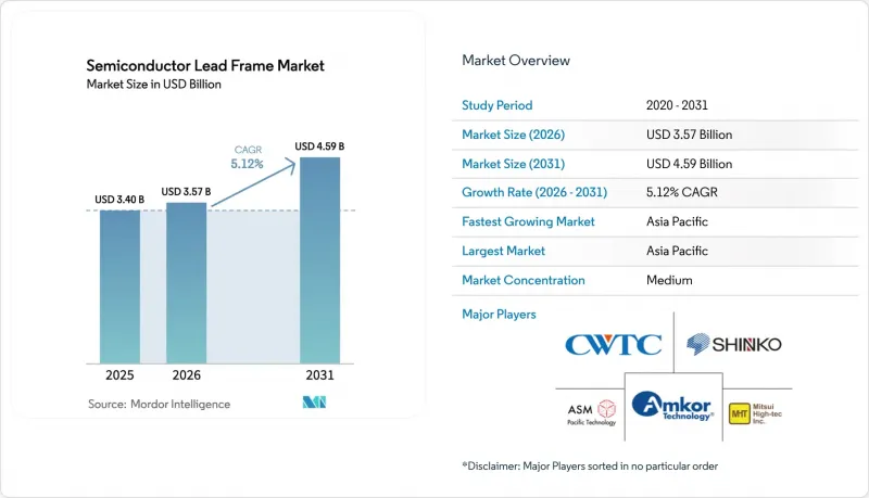
2025 年半導體導線架市場價值為 34 億美元,預計到 2031 年將達到 45.9 億美元,而 2026 年為 35.7 億美元,預測期(2026-2031 年)複合年成長率為 5.12%。
隨著汽車電子、5G基礎設施和人工智慧驅動的邊緣設備對能夠處理高速訊號並有效散熱的緊湊型封裝的需求加速成長。小型化技術的進步促使生產轉向四方扁平無引腳(QFN)和雙扁平無引腳(DFN)封裝,而電動汽車(EV)中功率電子技術的日益普及也提高了對能夠承受更高熱負荷的銅基封裝的要求。 CHIPS方法在北美和歐洲創造了新的產能,加速了供應鏈的地域多角化,並與亞太地區的現有生產基地結合。同時,旨在應對銅和銀價格波動以及支持碳化矽(SiC)和氮化鎵(GaN)技術的材料創新,推動了複合材料和多層結構的廣泛應用。
全球半導體導線架市場趨勢及洞察
家用電子電器的需求正在激增。
2024 年和 2025 年初智慧型手機、穿戴式裝置和遊戲裝置出貨量的激增縮短了產品開發週期,促使設計人員採用更薄的 QFN 封裝,從而在不增加裝置尺寸的情況下改善散熱路徑。目前,全球約四分之一的半導體裝置生產已採用厚度小於 0.1 毫米的導線架,從而提高了高階行動電話內部的元件密度。多家 OSAT 供應商已將其汽車級認證流程擴展至消費性電子產品線,推動了攜帶式產品(尤其是在頻繁溫度波動環境下)的 0 級可靠性。這些變化推動了半導體導線架市場的發展,因為設備製造商需要在電池續航時間、重量和性能之間取得平衡。
電動車和混合動力汽車用電力電子技術快速成長
隨著電動車 (EV) 產量激增,牽引逆變器的電壓架構已從 400V 過渡到 800V。這要求導線架採用導熱性和抗疲勞強度更高的銅合金。 ROHM 的 TRCDRIVE pack™ SiC 模組證明了最佳化熱擴散對於在高達 300kW 的功率下保持低開關損耗的必要性。一級供應商指定採用複合框架,將壓制銅與鎳鈀鍍層結合,以抑制車輛長期使用壽命期間的腐蝕。汽車產業採購需求的增加拓寬了半導體導線架市場的收入前景,並鞏固了長期訂單。
資本投資集中及生產瓶頸
精細間距承包沖壓生產線每個廠址造價超過3億美元,隨著晶片焊盤尺寸的縮小,模具成本也隨之上升。中小型供應商面臨融資緊張的困境,一些供應商選擇與大型外包半導體測試與製造(OSAT)企業合併或授權其產能。先進的自動化技術,包括準確率高達95%的人工智慧缺陷檢測網路,在一定程度上彌補了人手不足,但也延長了量產時間。產能緊張導致客戶認證延遲,對半導體導線架市場構成不利影響。
細分市場分析
2025年,QFN封裝佔總出貨量的31.65%,在基板面積有限的環境下,其散熱效率仍是最佳選擇。該領域引線間距和中心焊盤小型化的趨勢,提高了汽車感測器和高階智慧型手機的可靠性。預計到2031年,DFN封裝的複合年成長率將達到8.45%,其更薄的封裝尺寸使其更適用於穿戴式裝置和緊湊型物聯網終端節點。 QFN和DFN封裝共同維持了強勁的營收成長,支撐了半導體導線架市場的整體上升趨勢。
諸如嵌入式熱熔渣和雙晶片堆疊等技術進步拓展了QFP封裝的應用場景。同時,DIP和SOP封裝逐漸轉向傳統和工業市場,在這些市場中,成本優先於小型化。覆晶封裝支援高效能運算,但需要鍍銅柱而非裸露引腳。在這一領域,受智慧型手機型號不斷更新換代以及法規對輕量化汽車模組的需求推動,QFN和DFN半導體導線架市場規模預計將超過整個行業的成長率。
2025年,沖壓製程仍佔總產量的62.75%,這得益於每小時沖壓次數超過9萬次的高速沖床以及可縮短設定時間的模組化模具。連續帶材電鍍技術實現了選擇性表面處理,從而減少了貴金屬的使用。然而,隨著設計人員擴大將鉬和鋁嵌入銅芯中以增強散熱,預計到2031年,多層複合材料的複合年成長率將達到9.05%。這些高階配置反映了半導體導線架市場對電動車逆變器嚴苛運作條件的積極反應。
蝕刻技術在5G波束成形器和光學模組等小批量、高精度電路領域已佔據市場佔有率。雷射輔助光阻劑曝光提高了邊緣清晰度,並實現了±5µm的尺寸控制。面對日益複雜的工藝,半導體導線架行業已將研發重點轉向混合工藝流程,該流程採用蝕刻技術製造微結構,並採用沖壓技術增強機械強度,從而在縮短產品推出時間的緊迫壓力下,平衡成本和性能。
半導體導線架市場按封裝類型(DIP(雙列直插式封裝)、SOP(小外形封裝)等)、製造流程(沖壓導線架、蝕刻導線架等)、應用(積體電路、分立元件等)、產業(家用電子電器、汽車等)和地區(北美、南美、歐洲、亞太、中東和非洲)進行細分。
區域分析
預計到2025年,亞太地區將佔全球銷售額的41.10%,並將在2031年之前維持8.75%的複合年成長率。中國出貨超過420億個沖壓導線架,而日本精密蝕刻專家則為駕駛輔助系統提供了高頻模組。在越南和馬來西亞,超過3億美元的投資用於升級電鍍生產線,以滿足碳化矽動力混合動力系統的需求。
在北美,《晶片製造和創新法案》(CHIPS Act)注入了新的動力,撥款390億美元用於擴大製造地規模,132億美元用於研發。預計到2032年,晶圓廠產能將有所成長,這將催生對符合異質整合藍圖的國內採購架構的需求。英特爾的EMIB和Foveros專案需要獨特的銅合金成分,這需要一個能夠區分供應商的增值層級。
在總額達430億歐元(約499億美元)的《歐洲晶片法案》的支持下,歐洲致力於發展高可靠性的汽車和工業應用,該法案旨在2030年使歐洲半導體產量佔全球半導體產量的20%。由於本地積體電路基板製造能力有限,新參與企業得以在德國汽車製造商附近建立複合材料和蝕刻框架生產線。原物料價格上漲(銅價上漲9%,鋁價上漲8%)迫使歐洲企業探索符合減碳義務的回收措施,增強了半導體導線架產業供應鏈的韌性。
其他好處:
- Excel格式的市場預測(ME)表
- 3個月的分析師支持
目錄
第1章:引言
- 研究假設和市場定義
- 調查範圍
第2章:調查方法
第3章執行摘要
第4章 市場狀況
- 市場概覽
- 市場促進因素
- 家用電器需求激增。
- 電動車和混合動力車的電力電子技術蓬勃發展
- 需要QFN/QFP封裝的5G/AI邊緣設備
- 擴大亞太地區的生產能力
- SiC/GaN 模組更適合採用銅導線架。
- 《晶片包裝和包裝法案》(CHIPS Act)推動了國內包裝產業的資本投資。
- 市場限制因素
- 資本投資集中及生產瓶頸
- 銅和銀價格波動
- 向玻璃/有機中介層的過渡
- 加強電鍍化學品監管
- 價值鏈分析
- 監理情勢
- 技術展望
- 波特五力分析
- 新進入者的威脅
- 買方的議價能力
- 供應商的議價能力
- 替代品的威脅
- 競爭公司之間的競爭
- 投資趨勢(資本投資和併購)
- 對宏觀經濟因素的影響
第5章 市場規模與成長預測
- 按包裝類型
- DIP(雙列直插式封裝)
- SOP(小型外形封裝)
- SOT(小外形電晶體)
- QFP(四方扁平封裝)
- DFN(雙扁平無鉛)
- QFN(四方扁平無鉛)
- FC 和 TO 包裝
- 透過製造程序
- 壓印導線架
- 導線架蝕刻
- 多層/複合材料
- 透過使用
- 積體電路
- 分立元件
- 電源模組
- 微機電系統和感測器
- 按行業
- 家用電子電器
- 車
- 工業和家用電子電器
- 溝通
- 航太/國防
- 醫療設備
- 按地區
- 北美洲
- 美國
- 加拿大
- 南美洲
- 巴西
- 阿根廷
- 南美洲其他地區
- 歐洲
- 德國
- 英國
- 法國
- 義大利
- 俄羅斯
- 其他歐洲地區
- 亞太地區
- 中國
- 日本
- 韓國
- 印度
- ASEAN
- 亞太其他地區
- 中東和非洲
- 中東
- GCC
- 其他中東國家
- 非洲
- 南非
- 其他非洲地區
- 中東
- 北美洲
第6章 競爭情勢
- 市場集中度
- 策略趨勢
- 市佔率分析
- 公司簡介
- Mitsubishi Materials Corporation
- Amkor Technology Inc.
- SHINKO ELECTRIC INDUSTRIES CO., LTD.
- Precision Micro Ltd.
- Maxell, Ltd.
- ROHM MECHATECH
- Technic Inc.
- SDI Group, Inc.
- Dai Nippon Printing Co., Ltd.
- Sun Industry Co., Ltd.
- ECE
- Mitsui High-tec, Inc.
- ASM Pacific Technology Ltd.
- Chang Wah Technology Co., Ltd.
- Resonac Corporation
- Jentech Precision Industrial
- Nippon Micro Metal Corp.
- Hitek Fine Metal Co., Ltd.
- SDI Malaysia
- Possehl Electronics
- Jiangsu Hengxin Technology
- Haesung DS Co., Ltd.
- Carsem(M)Sdn Bhd
- Ningbo Kangqiang
第7章 市場機會與未來展望
The semiconductor lead frame market size was valued at USD 3.40 billion in 2025 and estimated to grow from USD 3.57 billion in 2026 to reach USD 4.59 billion by 2031, at a CAGR of 5.12% during the forecast period (2026-2031).
Demand accelerated as automotive electronics, 5G infrastructure, and AI-enabled edge devices required compact packages that dissipate heat effectively while supporting high-speed signals. Miniaturization shifted unit volumes toward Quad Flat No-Lead (QFN) and Dual Flat No-Lead (DFN) variants, and power-electronics adoption in electric vehicles (EVs) lifted specifications for copper-based frames able to endure higher thermal loads. Regionalization of supply chains gathered momentum as the CHIPS Act prompted fresh capacity in North America and Europe, complementing entrenched production hubs in Asia-Pacific. At the same time, composite and multi-layer structures gained traction as material innovations aimed to counter copper and silver price volatility and support silicon carbide (SiC) and gallium nitride (GaN) technologies.
Global Semiconductor Lead Frame Market Trends and Insights
Consumer-electronics demand spike
Surging smartphone, wearable, and gaming-device shipments in 2024 and early 2025 tightened product-development cycles and pushed designers toward slimmer QFN outlines that improved thermal paths without enlarging footprints. Roughly one quarter of global output already uses lead-frame thicknesses below 0.1 mm, enabling higher component density inside premium mobiles. Several OSAT providers extended automotive-qualified flows to consumer lines, promoting Grade-0 reliability in handheld products that faced frequent temperature swings. These shifts sustained the semiconductor lead frame market as device makers balanced battery life, weight, and performance requirements.
EV and xEV power-electronics boom
Electric-vehicle production climbed sharply, and traction inverters shifted from 400 V to 800 V architectures. Lead frames, therefore, require copper alloys with improved thermal conductivity and fatigue strength. ROHM's TRCDRIVE pack(TM) SiC module illustrated the need for optimized heat spreading to maintain low switching losses up to 300 kW. Tier-1 suppliers specified composite frames that paired stamped copper with plated nickel-palladium finishes to control corrosion over extended vehicle lifetimes. The automotive procurement wave broadened revenue visibility and anchored long-term orders within the semiconductor lead frame market.
CAPEX intensity and production bottlenecks
Turnkey stamping lines with fine-pitch capability exceeded USD 300 million per site, and tooling costs rose as die pads shrank. Smaller vendors faced liquidity strains, pushing some to merge or license capacity from larger OSATs. High automation levels, including AI-enabled defect-inspection networks with 95% accuracy, partially offset labour shortages but lengthened ramp timelines. Capacity tightness occasionally delays customer qualifications, creating a headwind for the semiconductor lead frame market.
Other drivers and restraints analyzed in the detailed report include:
- 5G/AI edge devices needing QFN/QFP
- Asia-Pacific capacity additions
- Copper and Ag price volatility
For complete list of drivers and restraints, kindly check the Table Of Contents.
Segment Analysis
QFN packages captured 31.65% of 2025 volumes, confirming their role as the preferred choice for thermal efficiency in limited board area. The segment's evolution toward smaller lead pitches and center pads bolstered reliability in automotive sensors and premium smartphones. DFN units, projected to deliver an 8.45% CAGR to 2031, offered even thinner profiles suited to wearables and compact IoT end-nodes. Together, QFN and DFN sustained healthy revenue streams that kept the semiconductor lead frame market on its upward trajectory.
Advances such as drop-in heat slugs and double-die stacking expanded QFP use cases, while DIP and SOP packages gradually migrated to legacy or industrial markets where cost outweighed miniaturization. Flip-chip outlines served high-performance computing but required plated copper pillars rather than exposed leads. Across the category, the semiconductor lead frame market size for QFN and DFN was forecast to outpace wider industry growth, driven by continuous smartphone refresh cycles and regulatory pushes for lighter in-car modules.
Stamping maintained 62.75% of 2025 production thanks to high-speed presses exceeding 90,000 strokes per hour and modular die sets that reduced changeover time. Continuous strip plating added selective finishes that limited precious-metal usage. Multi-layer composites, however, are expected to register a 9.05% CAGR through 2031 as designers combine copper cores with inlaid molybdenum or aluminium for thermal spreading. These premium configurations reflect the semiconductor lead frame market's response to EV inverter stress conditions.
Etching found a share in small-lot, high-precision circuits for 5G beamformers and optical modules. Laser-assisted photoresist exposure improved edge acuity, allowing +-5 µm dimensional control. As complexity rose, the semiconductor lead frame industry allocated research and development toward hybrid flows that used etching for fine features and stamping for mechanical robustness, balancing cost and performance under tightened product-launch windows.
Semiconductor Lead Frame Market is Segmented by Packaging Type (DIP (Dual In-Line Package), SOP (Small Outline Package), and More), Manufacturing Process (Stamping Lead Frame, Etching Lead Frame, and More), Application (Integrated Circuits, Discrete Devices, and More), Industry Vertical (Consumer Electronics, Automotive, and More), and Geography (North America, South America, Europe, Asia-Pacific, and Middle East and Africa).
Geography Analysis
Asia-Pacific held 41.10% of global revenue in 2025 and was expected to log a 8.75% CAGR through 2031. China shipped more than 42 billion stamped frames, while Japan's precision-etch specialists supplied high-frequency modules for driver-assistance systems. Investments exceeding USD 300 million in Vietnam and Malaysia upgraded plating lines to support SiC power hybrids.
North America saw renewed impetus from the CHIPS Act, which earmarked USD 39 billion for fabrication expansion and USD 13.2 billion for R&D. Fab capacity was projected to rise 203% by 2032, creating demand for domestically sourced frames that matched heterogeneous-integration roadmaps. Intel's EMIB and Foveros programs required custom copper-alloy compositions, adding value layers that differentiated suppliers.
Europe concentrated on high-reliability automotive and industrial uses, supported by the Euro 43 billion (USD 49.90 billion) European Chips Act, aiming for 20% global semiconductor output by 2030. Limited local IC-substrate capability left white-space for new entrants ready to establish composite or etched-frame lines near Germany's car manufacturers. Raw-material price escalation-copper up 9% and aluminium up 8%-drove European firms to explore recycling initiatives that aligned with carbon-reduction mandates, reinforcing supply-chain resilience in the semiconductor lead frame industry.
- Mitsubishi Materials Corporation
- Amkor Technology Inc.
- SHINKO ELECTRIC INDUSTRIES CO., LTD.
- Precision Micro Ltd.
- Maxell, Ltd.
- ROHM MECHATECH
- Technic Inc.
- SDI Group, Inc.
- Dai Nippon Printing Co., Ltd.
- Sun Industry Co., Ltd.
- ECE
- Mitsui High-tec, Inc.
- ASM Pacific Technology Ltd.
- Chang Wah Technology Co., Ltd.
- Resonac Corporation
- Jentech Precision Industrial
- Nippon Micro Metal Corp.
- Hitek Fine Metal Co., Ltd.
- SDI Malaysia
- Possehl Electronics
- Jiangsu Hengxin Technology
- Haesung DS Co., Ltd.
- Carsem (M) Sdn Bhd
- Ningbo Kangqiang
Additional Benefits:
- The market estimate (ME) sheet in Excel format
- 3 months of analyst support
TABLE OF CONTENTS
1 INTRODUCTION
- 1.1 Study Assumptions and Market Definition
- 1.2 Scope of the Study
2 RESEARCH METHODOLOGY
3 EXECUTIVE SUMMARY
4 MARKET LANDSCAPE
- 4.1 Market Overview
- 4.2 Market Drivers
- 4.2.1 Consumer-electronics demand spike
- 4.2.2 EV and xEV power-electronics boom
- 4.2.3 5G/AI edge devices needing QFN/QFP
- 4.2.4 Asia-Pacific capacity additions
- 4.2.5 SiC/GaN modules favour Cu lead frames
- 4.2.6 CHIPS-Act-driven on-shore packaging CAPEX
- 4.3 Market Restraints
- 4.3.1 CAPEX intensity and production bottlenecks
- 4.3.2 Copper and Ag price volatility
- 4.3.3 Shift to glass/organic interposers
- 4.3.4 Stricter plating-chemical regulations
- 4.4 Value Chain Analysis
- 4.5 Regulatory Landscape
- 4.6 Technological Outlook
- 4.7 Porter's Five Forces Analysis
- 4.7.1 Threat of New Entrants
- 4.7.2 Bargaining Power of Buyers
- 4.7.3 Bargaining Power of Suppliers
- 4.7.4 Threat of Substitutes
- 4.7.5 Intensity of Competitive Rivalry
- 4.8 Investment Landscape (CAPEX and M&A)
- 4.9 Impact on Macroeconomic factors
5 MARKET SIZE AND GROWTH FORECASTS (VALUE)
- 5.1 By Packaging Type
- 5.1.1 DIP (Dual In-Line Package)
- 5.1.2 SOP (Small Outline Package)
- 5.1.3 SOT (Small Outline Transistor)
- 5.1.4 QFP (Quad Flat Pack)
- 5.1.5 DFN (Dual Flat No-Lead)
- 5.1.6 QFN (Quad Flat No-Lead)
- 5.1.7 FC and TO Packages
- 5.2 By Manufacturing Process
- 5.2.1 Stamping Lead Frame
- 5.2.2 Etching Lead Frame
- 5.2.3 Multi-layer / Composite
- 5.3 By Application
- 5.3.1 Integrated Circuits
- 5.3.2 Discrete Devices
- 5.3.3 Power Modules
- 5.3.4 MEMS and Sensors
- 5.4 By Industry Vertical
- 5.4.1 Consumer Electronics
- 5.4.2 Automotive
- 5.4.3 Industrial and Commercial Electronics
- 5.4.4 Telecommunications
- 5.4.5 Aerospace and Defence
- 5.4.6 Medical Devices
- 5.5 By Geography
- 5.5.1 North America
- 5.5.1.1 United States
- 5.5.1.2 Canada
- 5.5.2 South America
- 5.5.2.1 Brazil
- 5.5.2.2 Argentina
- 5.5.2.3 Rest of South America
- 5.5.3 Europe
- 5.5.3.1 Germany
- 5.5.3.2 United Kingdom
- 5.5.3.3 France
- 5.5.3.4 Italy
- 5.5.3.5 Russia
- 5.5.3.6 Rest of Europe
- 5.5.4 Asia-Pacific
- 5.5.4.1 China
- 5.5.4.2 Japan
- 5.5.4.3 South Korea
- 5.5.4.4 India
- 5.5.4.5 ASEAN
- 5.5.4.6 Rest of Asia-Pacific
- 5.5.5 Middle East and Africa
- 5.5.5.1 Middle East
- 5.5.5.1.1 GCC
- 5.5.5.1.2 Rest of Middle East
- 5.5.5.2 Africa
- 5.5.5.2.1 South Africa
- 5.5.5.2.2 Rest of Africa
- 5.5.5.1 Middle East
- 5.5.1 North America
6 COMPETITIVE LANDSCAPE
- 6.1 Market Concentration
- 6.2 Strategic Moves
- 6.3 Market Share Analysis
- 6.4 Company Profiles (includes Global level Overview, Market level overview, Core Segments, Financials as available, Strategic Information, Market Rank/Share, Products and Services, Recent Developments)
- 6.4.1 Mitsubishi Materials Corporation
- 6.4.2 Amkor Technology Inc.
- 6.4.3 SHINKO ELECTRIC INDUSTRIES CO., LTD.
- 6.4.4 Precision Micro Ltd.
- 6.4.5 Maxell, Ltd.
- 6.4.6 ROHM MECHATECH
- 6.4.7 Technic Inc.
- 6.4.8 SDI Group, Inc.
- 6.4.9 Dai Nippon Printing Co., Ltd.
- 6.4.10 Sun Industry Co., Ltd.
- 6.4.11 ECE
- 6.4.12 Mitsui High-tec, Inc.
- 6.4.13 ASM Pacific Technology Ltd.
- 6.4.14 Chang Wah Technology Co., Ltd.
- 6.4.15 Resonac Corporation
- 6.4.16 Jentech Precision Industrial
- 6.4.17 Nippon Micro Metal Corp.
- 6.4.18 Hitek Fine Metal Co., Ltd.
- 6.4.19 SDI Malaysia
- 6.4.20 Possehl Electronics
- 6.4.21 Jiangsu Hengxin Technology
- 6.4.22 Haesung DS Co., Ltd.
- 6.4.23 Carsem (M) Sdn Bhd
- 6.4.24 Ningbo Kangqiang
7 MARKET OPPORTUNITIES AND FUTURE OUTLOOK
- 7.1 White-space and Unmet-need Assessment

