


 |
市場調查報告書
商品編碼
2035027
光掩模:市場佔有率分析、產業趨勢與統計、成長預測(2026-2031)Photomask - Market Share Analysis, Industry Trends & Statistics, Growth Forecasts (2026 - 2031) |
||||||
※ 本網頁內容可能與最新版本有所差異。詳細情況請與我們聯繫。
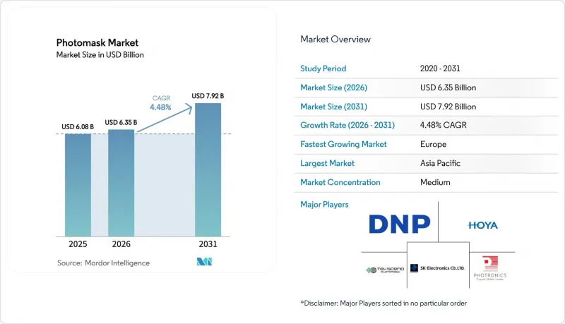
2025 年光罩市場價值為 60.8 億美元,預計到 2031 年將達到 79.2 億美元,而 2026 年為 63.5 億美元,預測期(2026-2031 年)複合年成長率為 4.48%。
對高解析度光掩模、更嚴格的關鍵尺寸 (CD) 控制以及無缺陷掩模坯的持續需求,推動了這一穩步成長。台灣和韓國高數值孔徑 (NA) EUV 設備的加速部署,推高了平均售價,因為隨著光刻節點的持續演進,需要更先進的移相技術和吸收層。半導體供應鏈在地化的全球趨勢也惠及了光掩模市場。美國和歐盟的新建晶圓廠為了最佳化資本效率,選擇外包使用商用掩模,而非自行生產。同時,基於晶片組的設計正逐步推動對線路重布(RDL) 和中介層掩模的需求,使光掩模的應用範圍從前端晶圓加工擴展到先進封裝。顯示面板製造商向第八代及以後的 AMOLED 生產線轉型,也進一步推動了市場成長,因為每條新生產線最多需要 30 個不同的顯示掩模,這增加了層數,提高了單廠收入。
全球光掩模市場趨勢及洞察
台灣及韓國引進高數值孔徑極紫外光刻微影術
高數值孔徑(NA)極紫外光刻(EUV)設備的積極應用表明,業界正邁入埃級時代,對光刻掩模製造商提出了低於10奈米的圖形精度和近乎零印刷缺陷的要求。台積電和三星目前為高NA光刻掩模支付的價格是傳統EUV設備的3到4倍,儘管產量持平,供應商的利潤卻在不斷成長。韓國4,710億美元的半導體產業叢集計畫包括建造自身的光刻掩模基礎設施,預計將減少對進口的依賴並重組區域物流系統。一旦出口限制放寬,中國二線代工廠預計也將效仿,儘管速度將稍微延遲。總而言之,這些趨勢將擴大尖端光刻掩模生產與傳統光刻掩模生產之間的技術差距,降低傳統光刻掩模的利潤率,同時提高高階產品的盈利。
美國和歐盟的《晶片和植入物保護法案》(CHIPS Acts)促進了口罩生產的外包。
美國一項價值527億美元的國內獎勵計劃,以及歐洲類似的措施,正在鼓勵規模較小、較新的晶圓廠建設自己的光掩模生產設施。作為回應,商業光掩模供應商正在亞利桑那州、俄亥俄州和德累斯頓等地的先進晶圓廠附近建造無塵室,從而縮短生產週期並增強抵禦地緣政治風險的能力。這種地域多角化趨勢降低了對亞太地區的過度依賴,在當前緊張局勢加劇的情況下,更是一種戰略上的必然選擇。早期的外包協議規定了專用於3奈米和2奈米製程節點的工具集,從而確保了長期的收入來源。隨著時間的推移,為了節省資金,越來越多的單體內部光掩模工廠被關閉,外部供應商的議價能力也隨之增強。
當 EUV 微影掩模坯的缺陷密度超過 5 個缺陷/cm² 時,廢品量就會增加。
當缺陷密度超過 5 個缺陷/平方公分的閾值時,晶圓廠將被迫報廢高達 25% 的 EUV 光掩模坯,導致每個掩模坯成本增加 5 萬至 10 萬美元,並延誤流片進度。認證供應商數量有限(主要為 AGC 和信越化學),且在滿足日益嚴格的規格要求的同時,難以擴大生產規模。雖然新的偵測光學元件和清洗製程正在降低顆粒數量,但能否將缺陷密度降至 2 個缺陷/平方公分以下仍存在不確定性。持續的報廢正在擠壓供應商的利潤空間,並給晶圓廠 2025-2026 年的量產計劃帶來壓力。長期的供不應求可能會導致高階光掩模的交付停滯,並減緩光掩模市場的複合年成長率。
細分市場分析
預計到2025年,光掩模將佔大部分銷售額,達到光罩市場的65.90%。這是因為在10nm以下的所有關鍵層中,為了保持線緣粗糙度符合規格,需要完美的影像轉移。高昂的價格源自於需要補償高級抗蝕劑的相互作用和相位偏移調整。隨著高數值孔徑極紫外光刻技術的進步,每個裝置層通常都需要客製化照明,從而增加了每片晶圓使用的光罩數量。主掩模的成長速度最快,複合年成長率達4.99%。這是因為多重圖形化製程需要高保真模板,以便使用步進重複方法製造子遮罩。複製掩模和子掩模仍然服務於傳統節點,但隨著先進節點的普及,它們的銷售成長正在放緩。整體而言,預計到2031年,光掩模和主掩模的市場規模將與晶圓開工數量保持同步成長。
DNP成功展示了適用於2nm以下製程的EUV光刻掩模,凸顯了產品創新如何確保競爭優勢。光刻掩模供應商目前正在整合基於人工智慧的缺陷預測技術,以降低重製率並縮短晶圓製造週期。在台灣和韓國等大規模生產基地,能夠提前備貨並在晶圓製造廠附近當日交付的供應商更受青睞,這刺激了對區域衛星工廠的投資。由於製程轉換成本高昂,一旦獲得技術認證,客戶忠誠度就能維持,跨製程世代的收入前景也能得到保障。
預計到2025年,二元鉻掩模將佔據光掩模市場最大的佔有率,達到43.90%,這得益於其經濟高效的製造程序,該工藝不僅支援65nm及更早節點,還能繼續支援大多數顯示層。即使在市場停滯時期,二元鉻掩模的持續重要性也能保障供應商的現金流。同時,EUV掩模的複合年成長率最高,達到5.29%,這主要得益於代工廠和整合裝置製造商(IDM)對3nm以下製程的擴展。每個EUV掩模的售價是光學鉻掩模的數倍,因此銷量較低,但收入卻在成長。衰減相移掩模和交替相移掩模可以補充關鍵層中的光流,而奈米壓印模板則憑藉其高通量、低成本的替代方案,在記憶體圖形化領域佔據了一席之地,該方案能夠容忍壓印的細微差異,同時保證特徵均勻性。
隨著記憶體製造商將部分層轉移到極紫外光刻(EUV)技術以實現更高密度而無需引入新的微影術技術,EUV光掩模的市場規模預計將會擴大。Canon的奈米壓印藍圖透過為某些應用提供替代方案,持續對EUV價格施加下行壓力,儘管EUV在圖案形狀方面仍保持著更高的柔軟性和產能。供應商正在平衡其產品組合,將資本投資集中在EUV所需的多光束寫入器和薄膜生產線,同時維持其鉻掩模的生產能力。
區域分析
到2025年,亞太地區將佔全球銷售額的71.10%。這主要得益於台灣、韓國和中國集中了最先進的晶圓廠和最強大的光掩模製造生態系統。光是台積電一家就佔全球晶圓代工收入的60%以上,每季都產生龐大的光掩模需求。諸如信越化學的石英基基板、NuFlare的多光束寫入器和Mycronic的修復工具等互補供應鏈,實現了本地採購並最大限度地降低了週期時間風險。儘管有出口限制,中國仍在其成熟製程節點上以兩位數的速度持續提高產能,確保了對光學鉻掩模的持續需求。韓國投資4,710億美元的叢集計畫將在2047年前進一步鞏固亞太地區的領先地位,該計畫將新建16座晶圓廠,每座晶圓廠都將配備其專屬的光掩模基礎設施。
歐洲是成長最快的地區,年複合成長率高達4.55%,這得益於歐盟《晶片法案》下政府對半導體自給自足計畫的資助。位於德勒斯登的Tekscend Photomask多光束系統將複雜掩模的曝光時間從數天縮短至數小時,這表明歐洲大陸已為先進節點生產做好準備。德國在該地區扮演著核心角色,蔡司SMT正在耶拿、奧伯科亨和韋茨拉爾擴展其掩模解決方案中心,並根據當地工藝需求客製化光學元件、掩模坯和曝光工藝。憑藉對汽車和工業晶片的戰略性關注,歐洲已擁有設計和系統方面的專業知識,從而推動了光掩模在國內的廣泛應用。
在北美,高達527億美元的《晶片製造法案》(CHIPS Act)獎勵正在推動亞利桑那州、俄亥俄州和紐約州的晶圓廠計畫建設。這為附近的掩模供應商創造了新的需求。光是台積電在亞利桑那州投資1,650億美元的工廠每年就將消耗數千張極紫外光刻掩模,促使亞洲和歐洲的供應商在那裡建立衛星工廠。英特爾專注於代工業務,不斷擴張其全球晶圓廠,並擁有多家專業晶圓廠,使其基本客群更加多元化。然而,北美的成本結構仍然高於亞太地區,因此利潤率依賴快速原型製作和現場缺陷分析等附加價值服務。
其他好處:
- Excel格式的市場預測(ME)表
- 3個月的分析師支持
目錄
第1章:引言
- 研究假設和市場定義
- 調查範圍
第2章:調查方法
第3章執行摘要
第4章 市場狀況
- 市場概覽
- 市場促進因素
- 台灣及韓國引進高數值孔徑極紫外光刻微影術
- 美國和歐盟的《CHIPS法案》鼓勵將市售口罩外包。
- AMOLED 第八代以上晶圓廠在 30 層顯示器掩模方面處於領先地位。
- ADAS和功率半導體:對小於28nm的大面積光掩模的需求
- 晶片組用 RDL 和中介層用光掩模的需求激增。
- 人工智慧驅動的缺陷偵測縮短了我們自有工廠的周轉時間 (TAT)。
- 市場限制因素
- EUV光刻掩模坯缺陷率超過5個缺陷/cm²,廢品率急遽上升
- 日本石英基基板供應瓶頸
- 對多光束寫入器的出口限制限制了中國
- 韓國和台灣電費上漲
- 產業生態系分析
- 技術展望
- 波特五力分析
- 供應商的議價能力
- 買方的議價能力
- 新進入者的威脅
- 替代品的威脅
- 競爭公司之間的競爭
第5章 市場規模與成長預測
- 依產品類型
- 分劃板(4倍/5倍)
- 大師面具
- 複製/子掩碼
- 依口罩類型
- 二元鉻掩模(BCM)
- 衰減相移掩模(Att-PSM)
- 交替相移掩模(Alt-PSM)
- 無鉻相位微影術掩模
- 極紫外光掩模
- 奈米壓印模板
- 透過使用
- 半導體和積體電路製造
- 65奈米或以上
- 45~28 nm
- 22~14 nm
- 10~7 nm
- 5 nm
- 最大可達 3 奈米
- 平面顯示器
- LCD
- AMOLED
- OLED微型顯示器
- MEMS感測器
- 高級封裝(RDL/中介層)
- 光電和矽光電
- 其他
- 半導體和積體電路製造
- 按最終用途行業分類
- 代工廠和整合開發模組
- 無晶圓設計公司
- 顯示面板製造商
- OSAT/先進包裝供應商
- 研究和學術機構
- 航太/國防
- 電信設備製造商
- 按地區
- 北美洲
- 美國
- 加拿大
- 墨西哥
- 歐洲
- 德國
- 英國
- 法國
- 北歐國家
- 其他歐洲地區
- 南美洲
- 巴西
- 南美洲其他地區
- 亞太地區
- 中國
- 日本
- 印度
- 東南亞
- 亞太其他地區
- 中東和非洲
- 中東
- GCC
- 土耳其
- 其他中東國家
- 非洲
- 南非
- 其他非洲地區
- 中東
- 北美洲
第6章 競爭情勢
- 市場集中度
- 策略趨勢
- 市佔率分析
- 公司簡介
- Tekscend Photomask Inc.(Toppan)
- Dai Nippon Printing Co., Ltd.
- Photronics, Inc.
- Hoya Corporation
- SK-Electronics Co., Ltd.
- Nippon Filcon Co., Ltd.
- Compugraphics International Ltd.
- Taiwan Mask Corporation
- Mycronic AB
- LG Innotek Co., Ltd.
- Advanced Mask Technology Center GmbH
- Shenzhen Qingyi Photomask Ltd.
- NuFlare Technology Inc.
- Canon Inc.
- IMS Nanofabrication GmbH
- Applied Materials, Inc.
- ASML Holding NV
- Fujifilm Holdings Corp.
- Advantest Corp.
- Vistec Electron Beam
- JENOPTIK AG
第7章 市場機會與未來展望
The photomask market size was valued at USD 6.08 billion in 2025 and estimated to grow from USD 6.35 billion in 2026 to reach USD 7.92 billion by 2031, at a CAGR of 4.48% during the forecast period (2026-2031).
Sustained demand for higher-resolution reticles, tighter critical-dimension control and defect-free mask blanks underpins this steady growth. Accelerated deployment of High-NA EUV tools in Taiwan and Korea is lifting average selling prices because every successive lithography node requires more sophisticated phase-shift engineering and absorber materials. The photomask market also benefits from the global push to localize semiconductor supply chains; new fabs in the United States and the European Union are choosing merchant mask outsourcing over in-house shops to optimize capital efficiency. Meanwhile, chiplet-based designs spur incremental demand for redistribution-layer (RDL) and interposer masks, spreading photomask consumption beyond front-end wafer processing into advanced packaging. Display panel makers moving to Gen 8+ AMOLED lines add another vector of growth because each new line consumes up to 30 unique display masks, elevating layer counts and revenue per fab.
Global Photomask Market Trends and Insights
High-NA EUV lithography adoption in Taiwan and Korea
Aggressive rollout of High-NA EUV tools marks the industry's transition into the angstrom era, forcing mask makers to deliver sub-10 nm pattern fidelity with near-zero printable defects. TSMC and Samsung now pay three to four times more per High-NA mask than for conventional EUV sets, expanding supplier revenue even as unit volumes stay stable. Korea's USD 471 billion semiconductor cluster plan includes captive photomask infrastructure, lowering import reliance and reshaping regional logistics. Tier-two foundries in China are expected to follow with delayed but inevitable adoption once export-control barriers ease. These developments collectively widen the technology gap between leading-edge and legacy photomask production, pushing legacy margins downward while boosting high-end profitability.
U.S./EU CHIPS Acts fueling merchant mask outsourcing
Domestic incentive programs worth USD 52.7 billion in the United States and comparable measures in Europe encourage new fabs that lack scale to build proprietary mask shops. Merchant suppliers are responding by colocating cleanrooms next to advanced fabs in Arizona, Ohio, and Dresden, improving cycle-times and geopolitical resilience. The regionalization thrust reduces over-dependence on Asia-Pacific sources, a strategic imperative amid rising tensions. Early outsourcing contracts stipulate dedicated toolsets for 3 nm and 2 nm nodes, locking in long-term revenue streams. Over time, merchant providers gain bargaining power as more single-site captive shops shutter to conserve capital.
EUV mask-blank defectivity above 5 defects/cm2 escalating scrap
Defect densities beyond the 5 defects/cm2 threshold force fabs to scrap up to 25% of EUV mask blanks, inflating costs by USD 50,000-100,000 each and delaying tape-out schedules. Limited qualified suppliers-mainly AGC and Shin-Etsu-struggle to scale volumes while meeting tighter specifications. Although new inspection optics and cleaning recipes lower particle counts, the road to sub-2 defects/cm2 remains uncertain. Persistent scrap erodes supplier margins and strains fab ramp-ups slated for 2025-2026. Any prolonged shortage could stall high-end mask deliveries and temper the photomask market CAGR.
Other drivers and restraints analyzed in the detailed report include:
- AMOLED Gen 8+ fabs driving 30-layer display masks
- Chiplet RDL and interposer photomasks upsurge
- Japan quartz-substrate supply bottlenecks
For complete list of drivers and restraints, kindly check the Table Of Contents.
Segment Analysis
Reticles generated the bulk of 2025 revenue, holding 65.90% of the photomask market, because every critical layer at sub-10 nm requires flawless image transfer to maintain line-edge roughness within spec. Premium pricing stems from the need to offset sophisticated resist interactions and phase-shift tuning. As High-NA EUV progresses, each device layer often demands bespoke illumination, expanding mask counts per wafer start. Master masks are growing fastest at a 4.99% CAGR because multi-patterning flows require high-fidelity templates that feed step-and-repeat daughter mask production. Copy and daughter masks still address legacy nodes but show subdued volume growth as advanced nodes take center stage. Collectively, the photomask market size for reticles and masters is expected to rise in tandem with wafer starts through 2031.
DNP's successful demonstration of EUV masks for beyond-2 nm processes underscores how product innovation secures competitive advantage. Reticle suppliers now integrate AI-based defect prediction to lower re-spin rates, improving fab cycle time. Volume manufacturing clusters in Taiwan and Korea favor vendors that can preload inventory near fabs for same-day deliveries, prompting investment in regional satellite sites. Given the high switching costs, customer loyalty remains strong once technical qualification is achieved, preserving revenue visibility across process generations.
Binary chrome masks held the largest 43.90% slice of the photomask market in 2025 thanks to cost-efficient manufacturing that continues to serve 65 nm and older nodes plus most display layers. Their enduring relevance anchors supplier cash flows during market lulls. EUV masks, however, carry the fastest 5.29% CAGR, fueled by sub-3 nm process ramps at foundries and IDMs. Each EUV mask sells at a multiple of optical chrome pricing, magnifying revenue despite lower unit volume. Attenuated and alternating phase-shift masks complement optical flows for critical layers, while nano-imprint templates establish a niche in memory patterning by offering high-throughput, low-cost alternatives when feature uniformity tolerates imprint variability.
The photomask market size for EUV products should expand as memory makers migrate select layers to EUV, adding density without new lithography options. Canon's nano-imprint roadmap keeps downward pressure on EUV pricing by signaling a substitute for specific applications, but EUV retains higher flexibility and throughput for diverse pattern geometries. Suppliers balance portfolios by keeping chrome capacity viable while funneling capital expenditures toward multibeam writers and pellicle lines required for EUV.
The Photomask Market Report is Segmented by Product Type (Reticle, Master Mask, and Copy/Daughter Mask), Mask Type (Binary Chrome Mask, Attenuated Phase Shift Mask, Alternating Phase Shift Mask, and More), Application (Semiconductor and IC Manufacturing, Flat-Panel Displays, and More), End-Use Industry (Foundries and IDMs, Fabless Design Houses, and More), and Geography. The Market Forecasts are Provided in Terms of Value (USD).
Geography Analysis
Asia-Pacific secured 71.10% of global sales in 2025 because Taiwan, Korea and China host the densest concentration of cutting-edge fabs and the most complete mask-making ecosystem. TSMC alone represents more than 60% of global foundry revenue, commanding massive reticle volumes each quarter. Complementary supply chains-quartz substrates from Shin-Etsu Chemical, multibeam writers from NuFlare and repair tools from Mycronic-enable same-region procurement, minimizing cycle-time risk. China continues adding mature-node capacity at a double-digit clip despite export constraints, ensuring ongoing demand for optical chrome masks. Korea's USD 471 billion cluster plan adds 16 new fabs through 2047, each with dedicated photomask infrastructure, reinforcing Asia-Pacific pre-eminence.
Europe is growing fastest at 4.55% CAGR as governments fund semiconductor sovereignty programs under the European Chips Act. Tekscend Photomask's multibeam installation in Dresden cuts writing time for complex masks from days to mere hours, signaling continental readiness for advanced-node production. Germany anchors the region through ZEISS SMT's expansion of mask-solutions sites in Jena, Oberkochen and Wetzlar, aligning optics, blanks and writing to local fab needs. Strategic focus rests on automotive and industrial chips, where Europe already wields design and systems expertise, augmenting domestic photomask uptake.
North America benefits from USD 52.7 billion in CHIPS Act incentives that spur fab projects in Arizona, Ohio and New York, creating fresh demand for proximate mask suppliers. TSMC's USD 165 billion Arizona complex alone will consume thousands of EUV masks annually, inviting both Asian and European vendors to establish local satellite operations. Intel's foundry push, GlobalFoundries' expansions and multiple specialty fabs together diversify the customer base. However, cost structures remain higher than in Asia-Pacific, so profit margins depend on value-added services such as rapid-turn prototypes and on-site defect analysis.
- Tekscend Photomask Inc. (Toppan)
- Dai Nippon Printing Co., Ltd.
- Photronics, Inc.
- Hoya Corporation
- SK-Electronics Co., Ltd.
- Nippon Filcon Co., Ltd.
- Compugraphics International Ltd.
- Taiwan Mask Corporation
- Mycronic AB
- LG Innotek Co., Ltd.
- Advanced Mask Technology Center GmbH
- Shenzhen Qingyi Photomask Ltd.
- NuFlare Technology Inc.
- Canon Inc.
- IMS Nanofabrication GmbH
- Applied Materials, Inc.
- ASML Holding N.V.
- Fujifilm Holdings Corp.
- Advantest Corp.
- Vistec Electron Beam
- JENOPTIK AG
Additional Benefits:
- The market estimate (ME) sheet in Excel format
- 3 months of analyst support
TABLE OF CONTENTS
1 INTRODUCTION
- 1.1 Study Assumptions and Market Definition
- 1.2 Scope of the Study
2 RESEARCH METHODOLOGY
3 EXECUTIVE SUMMARY
4 MARKET LANDSCAPE
- 4.1 Market Overview
- 4.2 Market Drivers
- 4.2.1 High-NA EUV Lithography Adoption in Taiwan and Korea
- 4.2.2 U.S./EU CHIPS Acts Fueling Merchant Mask Outsourcing
- 4.2.3 AMOLED Gen 8+ Fabs Driving 30-Layer Display Masks
- 4.2.4 ADAS and Power-SemiLess than 28 nm Demand for Large-Area Reticles
- 4.2.5 Chiplet RDL and Interposer Photomasks Upsurge
- 4.2.6 AI-Enabled Defect Inspection Cutting TAT for Captive Shops
- 4.3 Market Restraints
- 4.3.1 EUV Mask-Blank Defectivity Above 5 defects/cm2 Escalating Scrap
- 4.3.2 Japan Quartz-Substrate Supply Bottlenecks
- 4.3.3 Export Controls on Multi-Beam Writers Limiting China
- 4.3.4 Rising Electricity Tariffs in Korea and Taiwan
- 4.4 Industry Ecosystem Analysis
- 4.5 Technological Outlook
- 4.6 Porter's Five Forces Analysis
- 4.6.1 Bargaining Power of Suppliers
- 4.6.2 Bargaining Power of Buyers
- 4.6.3 Threat of New Entrants
- 4.6.4 Threat of Substitutes
- 4.6.5 Competitive Rivalry
5 MARKET SIZE AND GROWTH FORECASTS (VALUES)
- 5.1 By Product Type
- 5.1.1 Reticle (4X/5X)
- 5.1.2 Master Mask
- 5.1.3 Copy/Daughter Mask
- 5.2 By Mask Type
- 5.2.1 Binary Chrome Mask (BCM)
- 5.2.2 Attenuated Phase Shift Mask (Att-PSM)
- 5.2.3 Alternating Phase Shift Mask (Alt-PSM)
- 5.2.4 Chromeless Phase Lithography Mask
- 5.2.5 EUV Photomask
- 5.2.6 Nano-imprint Template
- 5.3 By Application
- 5.3.1 Semiconductor and IC Manufacturing
- 5.3.1.1 More than 65 nm
- 5.3.1.2 45-28 nm
- 5.3.1.3 22-14 nm
- 5.3.1.4 10-7 nm
- 5.3.1.5 5 nm
- 5.3.1.6 Upto 3 nm
- 5.3.2 Flat-Panel Displays
- 5.3.2.1 LCD
- 5.3.2.2 AMOLED
- 5.3.2.3 OLED Micro-display
- 5.3.3 MEMS Sensors
- 5.3.4 Advanced Packaging (RDL/Interposer)
- 5.3.5 Photonics and Silicon Photonics
- 5.3.6 Others
- 5.3.1 Semiconductor and IC Manufacturing
- 5.4 By End-use Industry
- 5.4.1 Foundries and IDMs
- 5.4.2 Fabless Design Houses
- 5.4.3 Display Panel Manufacturers
- 5.4.4 OSAT/Advanced Packaging Providers
- 5.4.5 Research and Academia
- 5.4.6 Aerospace and Defense
- 5.4.7 Telecommunications OEMs
- 5.5 By Geography
- 5.5.1 North America
- 5.5.1.1 United States
- 5.5.1.2 Canada
- 5.5.1.3 Mexico
- 5.5.2 Europe
- 5.5.2.1 Germany
- 5.5.2.2 United Kingdom
- 5.5.2.3 France
- 5.5.2.4 Nordics
- 5.5.2.5 Rest of Europe
- 5.5.3 South America
- 5.5.3.1 Brazil
- 5.5.3.2 Rest of South America
- 5.5.4 Asia-Pacific
- 5.5.4.1 China
- 5.5.4.2 Japan
- 5.5.4.3 India
- 5.5.4.4 South-East Asia
- 5.5.4.5 Rest of Asia-Pacific
- 5.5.5 Middle East and Africa
- 5.5.5.1 Middle East
- 5.5.5.1.1 Gulf Cooperation Council Countries
- 5.5.5.1.2 Turkey
- 5.5.5.1.3 Rest of Middle East
- 5.5.5.2 Africa
- 5.5.5.2.1 South Africa
- 5.5.5.2.2 Rest of Africa
- 5.5.5.1 Middle East
- 5.5.1 North America
6 COMPETITIVE LANDSCAPE
- 6.1 Market Concentration
- 6.2 Strategic Moves
- 6.3 Market Share Analysis
- 6.4 Company Profiles {(includes Global level Overview, Market level overview, Core Segments, Financials as available, Strategic Information, Market Rank/Share for key companies, Products and Services, and Recent Developments)}
- 6.4.1 Tekscend Photomask Inc. (Toppan)
- 6.4.2 Dai Nippon Printing Co., Ltd.
- 6.4.3 Photronics, Inc.
- 6.4.4 Hoya Corporation
- 6.4.5 SK-Electronics Co., Ltd.
- 6.4.6 Nippon Filcon Co., Ltd.
- 6.4.7 Compugraphics International Ltd.
- 6.4.8 Taiwan Mask Corporation
- 6.4.9 Mycronic AB
- 6.4.10 LG Innotek Co., Ltd.
- 6.4.11 Advanced Mask Technology Center GmbH
- 6.4.12 Shenzhen Qingyi Photomask Ltd.
- 6.4.13 NuFlare Technology Inc.
- 6.4.14 Canon Inc.
- 6.4.15 IMS Nanofabrication GmbH
- 6.4.16 Applied Materials, Inc.
- 6.4.17 ASML Holding N.V.
- 6.4.18 Fujifilm Holdings Corp.
- 6.4.19 Advantest Corp.
- 6.4.20 Vistec Electron Beam
- 6.4.21 JENOPTIK AG
7 MARKET OPPORTUNITIES AND FUTURE OUTLOOK
- 7.1 White-space and Unmet-Need Assessment
 光掩模市場預測至2034年-全球分析(依遮罩類型、材料、技術、遮罩尺寸、應用、最終使用者和地區分類)
 雷射光掩模市場規模、佔有率和成長分析:按產品類型、交易類型、基板材料、應用和地區分類-2026-2033年產業預測
 薄膜光掩模市場報告:趨勢、預測及競爭分析(至2035年)
 全球光掩模市場規模、佔有率、趨勢和成長分析報告(2026-2034)
 光掩模雷射修復系統市場:依產品類型、技術、最終用戶和應用分類-2026-2032年全球預測
 光掩模市場規模、佔有率、趨勢和預測:按產品類型、掩模加工類型、應用和地區分類(2026-2034 年)半導體掩模服務市場:依最終用戶、應用、製程節點、服務、掩模類型和晶圓尺寸分類,全球預測,2026-2032年全球先進光掩模技術市場:預測(至2034年)-按類型、材料、技術、應用、最終用戶和地區分類的分析
 2026年全球雷射光掩模市場報告全球晶片光掩模市場報告(2026 年)