


 |
市場調查報告書
商品編碼
1940792
高階半導體封裝:市場佔有率分析、產業趨勢與統計、成長預測(2026-2031)High-End Semiconductor Packaging - Market Share Analysis, Industry Trends & Statistics, Growth Forecasts (2026 - 2031) |
||||||
※ 本網頁內容可能與最新版本有所差異。詳細情況請與我們聯繫。
預計到 2026 年,高階半導體封裝市場規模將達到 478.8 億美元,高於 2025 年的 415.7 億美元。
預計到 2031 年,該產業規模將達到 970.8 億美元,2026 年至 2031 年的複合年成長率為 15.18%。
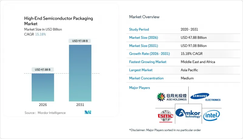
大量資本流入異質整合領域、人工智慧加速器需求激增以及基板技術的創新共同支撐著強勁的成長勢頭。垂直代工一體化加劇了傳統外包組裝和測試 (OSAT) 供應商的競爭壓力,同時也縮短了人工智慧晶片的上市時間。智慧型手機和汽車系統晶片(SoC) 供應商向 5 奈米及以下過程的轉型,推動了對扇出型和矽中介層平台的需求成長。從美國的《晶片整合與保護法案》(CHIPS Act) 到歐洲的 APECS 中心,一系列區域性政策獎勵正在重塑區域供應鏈結構,並鼓勵跨國公司實現先進封裝佈局的多元化。同時,基板短缺和熱密度限制制約了近期產能擴張,但也為能夠緩解這些瓶頸的設備製造商和材料專家創造了機會。
全球高階半導體封裝市場趨勢與洞察
對人工智慧/機器學習加速器的需求不斷成長
超大規模資料中心營運商正在向多晶片AI處理器轉型,這些處理器將功耗超過1000W的運算單元與堆疊式高頻寬記憶體相結合,對高階半導體封裝市場的先進溫度控管和供電提出了前所未有的要求。晶圓級晶片封裝(CoWoS)和類似中介層平台的產能仍然緊張,使得封裝交付前置作業時間成為AI產品發布的關鍵環節。代工廠正在利用系統級晶圓(SoC)概念,承諾提供比現有GPU高10倍的記憶體頻寬,這進一步加劇了散熱設計的挑戰。掌握了翹曲控制、微凸塊可靠性和液冷基板技術的供應商正在獲得定價權,使超大規模資料中心業者能夠按時完成部署。因此,系統架構師現在將封裝能力視為決定AI訓練成本和所需時間的關鍵因素。
向智慧型手機先進製程的過渡
隨著高階智慧型手機晶片製造商向3nm和2nm製程節點過渡,晶圓成本的上升迫使扇出型晶圓層次電子構裝和嵌入式橋接封裝技術同步發展,以在成本限制內實現高性能。受江森自控等公司斥資6.24億美元擴建產能的推動,中國智慧型手機製造商正加速採用國內OSAT服務,以實現價值鏈在地化並分散地緣政治風險。更小製程節點帶來的功耗控制提升,意味著更長的電池續航時間和更豐富的設備端AI體驗。然而,較小的間距需要小於2µm的線間距和超薄介電層的線路重布。在聚合物化學和電漿蝕刻技術方面不斷創新的設備供應商,正透過實現這些更精細結構的高產量比率而獲得競爭優勢。
資本密集度提高
預計到2023年,產業資本密集度將從2015年的18%上升至30%,並持續高於30%,因為下一代封裝生產線需要相容於極微影術的無塵室和後端設備,這些設備的成本高達數億美元。中型OSAT公司正面臨財務壓力,這促使它們進行整合,並與資金雄厚的代工廠成立合資企業。如今,資本支出已與前端晶圓廠的支出不相上下,預計到2033年,整個產業的資本支出將超過4,600億美元。即使是像ASMPT這樣的大型設備製造商,也報告稱其2024年的收入下降了10%,凸顯了資本密集型週期固有的波動性。從長遠來看,只有那些擁有地域多元化營運、規模優勢和差異化製程智慧財產權的公司,才能在各個技術節點上持續進行投資。
細分市場分析
到2025年,2.5D中介層將佔據高階半導體封裝市場最大的佔有率,因為設計公司優先考慮的是大規模生產中已驗證的產量比率和可製造性。這項技術將頻寬晶粒與HBM晶粒融合在一起,使GPU和FPGA在適中的熱負載下能夠實現數太比特每秒的Terabit。同時,規模較小的3D系統晶片)市場預計將以16.15%的複合年成長率快速成長,這主要得益於雲端和邊緣設備中人工智慧推理應用場景的推動,這些場景需要將邏輯和記憶體堆疊共置。隨著這些架構的日趨成熟,供應商正在最佳化晶粒通訊協定以降低垂直訊號傳輸延遲,從而加速其普及應用。
雖然中介層需求提高了基板供應商的收入可見性,但ABF(整合基板)前置作業時間風險的增加推動了人們對玻璃基和矽基中介層的興趣。同時,3D堆疊式記憶體封裝擴大了高頻寬記憶體供應商的可尋址範圍,增強了規模經濟效益。諸如Intel EMIB之類的嵌入式橋接方案無需使用複雜的完整中介層即可實現小於55µm的晶片晶粒,為異構整合提供了低成本的切入點。在該細分市場的高階半導體封裝領域,製程控制創新,特別是混合鍵結定位精度,仍是關鍵的差異化因素。
到2025年,覆晶球柵陣列(FBGA)將佔據高階半導體封裝市場42.65%的佔有率,這主要得益於其成熟的製造基礎和久經考驗的可靠性指標。伺服器CPU和GPU晶片的持續成長將支撐其產量,即便其他平台不斷湧現。面板級封裝(PLP)到2031年將以16.32%的複合年成長率成長,因為更大的基板尺寸能夠實現更高的單晶粒數量,從而降低移動和物聯網SoC的單位成本。三星的試驗生產線已經能夠處理600毫米的玻璃面板,超過了其300毫米晶圓的產能,並對傳統晶圓層次電子構裝的經濟性構成了威脅。
晶片級封裝 (PLP) 的應用受到邊緣翹曲和晶粒放置精度等挑戰的限制,迫使供應商改進真空吸盤和視覺對準系統。系統級封裝 (SiP) 解決方案正擴展到汽車雷達模組領域,透過整合天線和電源管理 IC 來縮小基板面積。在行動裝置領域,晶圓級晶片級封裝 (WL-CSP) 滿足了 Z 軸高度要求和成本目標,從而維持了市場需求。隨著高階半導體封裝市場的不斷發展,製造商擴大採用混合平台晶圓廠來滿足每種設計的成本、性能和可靠性要求。
這份高階半導體封裝報告按技術(例如,3D系統晶片、3D堆疊記憶體)、封裝平台(例如,覆晶球柵陣列、晶圓級晶片封裝)、裝置節點(例如,3nm以下、4-5nm)、最終用戶(例如,家用電子電器、通訊和5G基礎設施)以及地區進行細分。市場預測以美元計價。
區域分析
到2025年,亞太地區將佔據高階半導體封裝市場58.85%的佔有率,這主要得益於台灣在晶圓代工領域的主導地位、韓國在記憶體技術方面的專長以及中國OSAT(外包組裝、測試和封裝)基礎設施的快速發展。台積電、日月光和星輝半導體正將其後端生產線與前端晶圓廠毗鄰而建,從而縮短生產週期並降低物流成本。同時,北京的優惠政策培育了國內產業生態系統,中國的目標是到2030年實現國內封裝產能佔全球38%的佔有率,但出口管制政策增加了地緣政治的不確定性。
北美正著力發展高價值人工智慧和國防級封裝技術,其中520億美元的《晶片法案》(CHIPS Act)資金支持了安姆科(Amcor)位於亞利桑那州價值20億美元的工廠以及英特爾位於俄亥俄州的封裝超級基地。該地區設備和材料供應商的高度集中,使得下一代技術的快速原型開發成為可能。歐洲則致力於策略自主,並已開發出耗資7.3億歐元的APECS和8.3億歐元的FAMES開放式原型生產線,為中小企業提供價格合理的生產空間,並培育出覆蓋整個歐洲大陸的晶片生態系統。
預計到2031年,中東和非洲地區的複合年成長率將達到18.05%,這主要得益於主權財富基金對電信基礎設施部署和半導體中心的投資。阿拉伯聯合大公國等國正與全球OSAT(合約組裝、測試和組裝)公司合作,共同出資建設試點生產線,以滿足該地區對邊緣人工智慧模組的需求。南美洲雖然仍處於發展階段,但巴西家用電子電器的契約製造正在推動對在地化測試和成品加工服務的需求成長。這種地域格局凸顯了企業發展思維的轉變,即從單純的成本邊際收益轉向對韌性和國家安全的考量。
其他福利:
- Excel格式的市場預測(ME)表
- 3個月的分析師支持
目錄
第1章 引言
- 研究假設和市場定義
- 調查範圍
第2章調查方法
第3章執行摘要
第4章 市場情勢
- 市場概覽
- 市場促進因素
- 對人工智慧/機器學習加速器的需求不斷成長
- 智慧型手機向高階處理節點的遷移
- IDM/OSAT異質整合藍圖
- 晶片組在低地球軌道衛星有效載荷中的應用
- 用於高效能運算的晶片-晶圓-基板(CoWoS-R)光刻掩模的生長
- 歐洲政府資助的「超越莫耳定律」試點生產線
- 市場限制
- 資本密集度提高
- 5奈米製程之後,產量比率管理變得更加複雜。
- 有機中介體基板供應瓶頸
- 3D-SoC堆疊結構中散熱不均勻
- 產業價值鏈分析
- 監管環境
- 技術展望
- 波特五力分析
- 供應商的議價能力
- 買方的議價能力
- 新進入者的威脅
- 替代品的威脅
- 競爭程度
- 宏觀經濟影響評估
第5章 市場規模與成長預測
- 透過技術
- 3D系統晶片(3D-SoC)
- 3D堆疊式記憶體(HBM、HBM-PIM)
- 2.5D 中介層
- 超高密度扇出 (UHD-FO)
- 嵌入式矽橋/EMIB
- 透過包裝平台
- 覆晶球柵陣列(FC-BGA)
- 晶圓級晶片封裝(WLCSP)
- 面板級包裝(PLP)
- 系統級封裝(SiP)
- 按設備節點
- 3奈米或更小
- 4-5 nm
- 6-7 nm
- 10奈米或更大
- 最終用戶
- 家用電子電器
- 電信和5G基礎設施
- 汽車和ADAS
- 航太/國防
- 醫療設備
- 按地區
- 北美洲
- 美國
- 加拿大
- 墨西哥
- 南美洲
- 巴西
- 阿根廷
- 哥倫比亞
- 南美洲其他地區
- 歐洲
- 英國
- 德國
- 法國
- 義大利
- 西班牙
- 其他歐洲地區
- 亞太地區
- 中國
- 日本
- 韓國
- 印度
- 亞太其他地區
- 中東和非洲
- 中東
- 沙烏地阿拉伯
- 阿拉伯聯合大公國
- 其他中東地區
- 非洲
- 南非
- 埃及
- 其他非洲地區
- 中東
- 北美洲
第6章 競爭情勢
- 市場集中度
- 策略趨勢
- 市佔率分析
- 公司簡介
- Advanced Semiconductor Engineering Inc.(ASE Technology Holding Co., Ltd.)
- Amkor Technology, Inc.
- Intel Corporation
- Taiwan Semiconductor Manufacturing Company Limited(TSMC)
- Samsung Electronics Co., Ltd.
- JCET Group Co., Ltd.
- Siliconware Precision Industries Co., Ltd.(SPIL)
- Powertech Technology Inc.(PTI)
- TongFu Microelectronics Co., Ltd.
- Fujitsu Limited
- Texas Instruments Incorporated
- United Microelectronics Corporation(UMC)
- STATS ChipPAC Pte Ltd.
- Hiksemi Microelectronics Co., Ltd.
- Nanium SA(Infineon Backend)
- Chip MOS Technologies Inc.
- Taiwan Advanced Packaging Corporation(TAPC)
- Unimicron Technology Corp.
- Shinko Electric Industries Co., Ltd.
- Kyocera Corporation(AVX)
第7章 市場機會與未來展望
The high-end semiconductor packaging market size in 2026 is estimated at USD 47.88 billion, growing from 2025 value of USD 41.57 billion with 2031 projections showing USD 97.08 billion, growing at 15.18% CAGR over 2026-2031.
Robust capital flows toward heterogeneous integration, surging AI accelerator demand, and substrate innovations together reinforce a strong growth trajectory. Foundry vertical integration amplifies competitive pressure on traditional outsourced assembly and test (OSAT) vendors while improving time-to-market for AI chips. Sub-5 nm migration by smartphone and automotive system-on-chip (SoC) suppliers fuels incremental volume for fan-out and silicon interposer platforms. Regional policy incentives, from the U.S. CHIPS Act to Europe's APECS hub, are reshaping supply-chain geography, prompting multinational firms to diversify advanced packaging footprints. Meanwhile, substrate shortages and thermal-density limits temper near-term capacity ramps but simultaneously open opportunities for toolmakers and materials specialists that mitigate these bottlenecks.
Global High-End Semiconductor Packaging Market Trends and Insights
Rising Demand for AI/ML Accelerators
Hyperscale data-center operators pivot to multi-die AI processors that fuse >1,000 W compute tiles with stacked high-bandwidth memory, driving an unprecedented requirement for advanced thermal and power delivery inside the high-end semiconductor packaging market. Capacity for CoWoS and similar interposer platforms remains tight, elevating packaging lead-times to critical-path status for AI product launches. Foundries leveraging system-on-wafer concepts promise 10X memory bandwidth over current GPUs, further intensifying thermal engineering challenges. Vendors that master warpage control, micro-bump reliability, and liquid-coolable substrates gain pricing power as they enable hyperscalers to meet rollout schedules. Consequently, packaging capability is now viewed by system architects as a primary determinant of AI training cost and time.
Smartphone Migration to Advanced Nodes
Premium smartphone chipmakers are transitioning toward 3 nm and 2 nm production nodes, but rising wafer cost forces parallel advances in fan-out wafer-level and embedded bridge packaging to deliver performance within cost envelopes. Chinese handset brands accelerate adoption of domestic OSAT services following capacity acquisitions such as JCET's USD 624 million expansion, localizing value chains, and balancing geopolitical risk. Power-budget gains derived from finer nodes translate into longer battery life and richer on-device AI experiences; however, the tighter pitch requires redistribution layers with sub-2 µm line-and-space and ultra-thin dielectrics. Equipment suppliers innovating in polymer chemistries and plasma etch achieve a competitive advantage by enabling high volume yields at these geometries.
Escalating Capital Intensity
Industry capital intensity climbed from 18% in 2015 to 30% in 2023 and is expected to remain above 30% as next-generation packaging lines require EUV-litho-grade cleanrooms and back-end tools costing hundreds of millions of dollars. Mid-tier OSATs face balance-sheet stress, prompting consolidation or joint ventures with foundries wielding deep pockets. Equipment expenditures now rival front-end fab outlays, with projections exceeding USD 460 billion industry-wide by 2033. Even leading toolmakers such as ASMPT reported 10% revenue contraction in 2024, underscoring the volatility inherent in capex-heavy cycles. In the long term, only geographically diversified players with scale and differentiated process IP can fund successive technology nodes.
Other drivers and restraints analyzed in the detailed report include:
- Heterogeneous Integration Road-maps of IDMs/OSATs
- Growth of CoWoS-R for HPC Reticles
- Yield Management Complexity Beyond 5 nm
For complete list of drivers and restraints, kindly check the Table Of Contents.
Segment Analysis
2.5 D interposers captured the largest slice of the high-end semiconductor packaging market in 2025 as design houses prioritized proven yield and manufacturability at volume. The technology fuses logic and HBM dies with a moderate thermal penalty, supporting multi-terabit per second bandwidth in GPUs and FPGAs. By contrast, the 3D System-on-Chip segment, though smaller, is projected to clock the fastest 16.15% CAGR, underpinned by AI inference use cases in cloud and edge appliances that require co-located logic and memory stacks. As these architectures mature, vendors are optimizing die-to-die communication protocols to alleviate vertical signaling latency, accelerating broader adoption.
Interposer demand boosts revenue visibility for substrate suppliers, but mounting ABF lead-time risk has propelled interest in glass and silicon-based interposers. Meanwhile, 3D stacked-memory packages broaden the addressable base for high-bandwidth memory vendors, reinforcing scale economies. Embedded-bridge methods like Intel EMIB achieve die-to-die pitch <55 µm without full interposer complexity, offering a lower-cost entry point for heterogeneous integration. Within the high-end semiconductor packaging market size for this segment, process control innovations-especially hybrid bonding align accuracy-remain primary differentiators.
Flip-chip ball-grid-array held 42.65% of the high-end semiconductor packaging market share in 2025, thanks to an entrenched manufacturing base and well-documented reliability metrics. Continued growth in server CPUs and GPU tiles sustains volumes even as alternative platforms emerge. Panel-level packaging (PLP) rides a 16.32% CAGR through 2031 because larger substrate form factors permit more dies per carrier, lowering cost per unit for mobile and IoT SoCs. Samsung's pilot lines already process 600 mm glass panels, outpacing 300 mm wafer throughput and threatening traditional wafer-level economics.
PLP adoption is constrained by edge-warpage and die-placement accuracy challenges, compelling equipment vendors to refine vacuum-chuck and vision-alignment systems. System-in-Package solutions extend to automotive radar modules, integrating antennas and power management ICs to trim board area. In mobile devices, wafer-level chip-scale packages meet z-height mandates and cost goals, preserving demand momentum. As the high-end semiconductor packaging market evolves, manufacturers increasingly run mixed-platform fabs to align each design's cost, performance, and reliability envelope.
The High-End Semiconductor Packaging Report is Segmented by Technology (3D System-On-Chip, 3D Stacked Memory, and More), Packaging Platform (Flip-Chip Ball-Grid-Array, Wafer-Level Chip-Scale Package, and More), Device Node (Less Than or Equal To 3 Nm, 4-5 Nm, and More), End User (Consumer Electronics, Telecom and 5G Infrastructure, and More), and Geography. The Market Forecasts are Provided in Terms of Value (USD).
Geography Analysis
Asia-Pacific controlled 58.85% of the high-end semiconductor packaging market in 2025, anchored by Taiwan's foundry leadership, South Korea's memory expertise, and China's rapid OSAT build-out. TSMC, ASE Technology, and SPIL co-locate back-end lines next to front-end fabs, compressing cycle time and lowering logistic overhead. Simultaneously, Beijing's incentives foster a domestic ecosystem targeting 38% of global installed packaging capacity by 2030, though export-control policies add geopolitical uncertainty.
North America concentrates on high-value AI and defense-grade packages, buoyed by USD 52 billion CHIPS funding that subsidizes Amkor's USD 2 billion Arizona facility and Intel's Ohio packaging megasite. The region also houses a dense cluster of equipment and materials suppliers, allowing rapid prototyping for next-generation technologies. Europe pursues strategic autonomy through €730 million APECS and €830 million FAMES open-access pilot lines, giving SMEs affordable fabrication slots and seeding a continental chiplet ecosystem.
The Middle East and Africa chart an 18.05% CAGR through 2031, propelled by telecom infrastructure rollouts and sovereign funds investing in semiconductor hubs. Countries such as the United Arab Emirates partner with global OSATs to co-finance pilot lines, targeting regional demand for edge AI modules. South America remains nascent but benefits from consumer-electronics contract manufacturing in Brazil, generating incremental demand for localized test and finish services. The geographic mosaic underscores a shift from pure cost arbitrage toward resilience and national-security considerations.
- Advanced Semiconductor Engineering Inc. (ASE Technology Holding Co., Ltd.)
- Amkor Technology, Inc.
- Intel Corporation
- Taiwan Semiconductor Manufacturing Company Limited (TSMC)
- Samsung Electronics Co., Ltd.
- JCET Group Co., Ltd.
- Siliconware Precision Industries Co., Ltd. (SPIL)
- Powertech Technology Inc. (PTI)
- TongFu Microelectronics Co., Ltd.
- Fujitsu Limited
- Texas Instruments Incorporated
- United Microelectronics Corporation (UMC)
- STATS ChipPAC Pte Ltd.
- Hiksemi Microelectronics Co., Ltd.
- Nanium S.A. (Infineon Backend)
- Chip MOS Technologies Inc.
- Taiwan Advanced Packaging Corporation (TAPC)
- Unimicron Technology Corp.
- Shinko Electric Industries Co., Ltd.
- Kyocera Corporation (AVX)
Additional Benefits:
- The market estimate (ME) sheet in Excel format
- 3 months of analyst support
TABLE OF CONTENTS
1 INTRODUCTION
- 1.1 Study Assumptions and Market Definition
- 1.2 Scope of the Study
2 RESEARCH METHODOLOGY
3 EXECUTIVE SUMMARY
4 MARKET LANDSCAPE
- 4.1 Market Overview
- 4.2 Market Drivers
- 4.2.1 Rising demand for AI/ML accelerators
- 4.2.2 Smartphone migration to advanced nodes
- 4.2.3 Heterogeneous integration road-maps of IDMs/OSATs
- 4.2.4 Adoption of chip-lets for LEO satellite payloads
- 4.2.5 Growth of Chip-on-Wafer-on-Substrate (CoWoS-R) for HPC reticles
- 4.2.6 Government-funded 'More-than-Moore' pilot lines in Europe
- 4.3 Market Restraints
- 4.3.1 Escalating capital intensity
- 4.3.2 Yield management complexity beyond 5 nm
- 4.3.3 Sub-strate supply bottlenecks for organic interposers
- 4.3.4 Non-uniform thermal dissipation in 3D-SoC stacks
- 4.4 Industry Value Chain Analysis
- 4.5 Regulatory Landscape
- 4.6 Technological Outlook
- 4.7 Porter's Five Forces Analysis
- 4.7.1 Bargaining Power of Suppliers
- 4.7.2 Bargaining Power of Buyers
- 4.7.3 Threat of New Entrants
- 4.7.4 Threat of Substitutes
- 4.7.5 Degree of Competition
- 4.8 Assessment of Macroeconomic Impact
5 MARKET SIZE AND GROWTH FORECASTS (VALUE)
- 5.1 By Technology
- 5.1.1 3D System-on-Chip (3D-SoC)
- 5.1.2 3D Stacked Memory (HBM, HBM-PIM)
- 5.1.3 2.5D Interposers
- 5.1.4 Ultra-High-Density Fan-Out (UHD-FO)
- 5.1.5 Embedded Si Bridge / EMIB
- 5.2 By Packaging Platform
- 5.2.1 Flip-Chip Ball-Grid-Array (FC-BGA)
- 5.2.2 Wafer-Level Chip-Scale Package (WLCSP)
- 5.2.3 Panel-Level Packaging (PLP)
- 5.2.4 System-in-Package (SiP)
- 5.3 By Device Node
- 5.3.1 Less than or Equal to 3 nm
- 5.3.2 4-5 nm
- 5.3.3 6-7 nm
- 5.3.4 Greater than or Equal to 10 nm
- 5.4 By End User
- 5.4.1 Consumer Electronics
- 5.4.2 Telecom and 5G Infrastructure
- 5.4.3 Automotive and ADAS
- 5.4.4 Aerospace and Defense
- 5.4.5 Medical Devices
- 5.5 By Geography
- 5.5.1 North America
- 5.5.1.1 United States
- 5.5.1.2 Canada
- 5.5.1.3 Mexico
- 5.5.2 South America
- 5.5.2.1 Brazil
- 5.5.2.2 Argentina
- 5.5.2.3 Colombia
- 5.5.2.4 Rest of South America
- 5.5.3 Europe
- 5.5.3.1 United Kingdom
- 5.5.3.2 Germany
- 5.5.3.3 France
- 5.5.3.4 Italy
- 5.5.3.5 Spain
- 5.5.3.6 Rest of Europe
- 5.5.4 Asia-Pacific
- 5.5.4.1 China
- 5.5.4.2 Japan
- 5.5.4.3 South Korea
- 5.5.4.4 India
- 5.5.4.5 Rest of Asia-Pacific
- 5.5.5 Middle East and Africa
- 5.5.5.1 Middle East
- 5.5.5.1.1 Saudi Arabia
- 5.5.5.1.2 United Arab Emirates
- 5.5.5.1.3 Rest of Middle East
- 5.5.5.2 Africa
- 5.5.5.2.1 South Africa
- 5.5.5.2.2 Egypt
- 5.5.5.2.3 Rest of Africa
- 5.5.5.1 Middle East
- 5.5.1 North America
6 COMPETITIVE LANDSCAPE
- 6.1 Market Concentration
- 6.2 Strategic Moves
- 6.3 Market Share Analysis
- 6.4 Company Profiles (includes Global level Overview, Market level overview, Core Segments, Financials as available, Strategic Information, Market Rank/Share, Products and Services, Recent Developments)
- 6.4.1 Advanced Semiconductor Engineering Inc. (ASE Technology Holding Co., Ltd.)
- 6.4.2 Amkor Technology, Inc.
- 6.4.3 Intel Corporation
- 6.4.4 Taiwan Semiconductor Manufacturing Company Limited (TSMC)
- 6.4.5 Samsung Electronics Co., Ltd.
- 6.4.6 JCET Group Co., Ltd.
- 6.4.7 Siliconware Precision Industries Co., Ltd. (SPIL)
- 6.4.8 Powertech Technology Inc. (PTI)
- 6.4.9 TongFu Microelectronics Co., Ltd.
- 6.4.10 Fujitsu Limited
- 6.4.11 Texas Instruments Incorporated
- 6.4.12 United Microelectronics Corporation (UMC)
- 6.4.13 STATS ChipPAC Pte Ltd.
- 6.4.14 Hiksemi Microelectronics Co., Ltd.
- 6.4.15 Nanium S.A. (Infineon Backend)
- 6.4.16 Chip MOS Technologies Inc.
- 6.4.17 Taiwan Advanced Packaging Corporation (TAPC)
- 6.4.18 Unimicron Technology Corp.
- 6.4.19 Shinko Electric Industries Co., Ltd.
- 6.4.20 Kyocera Corporation (AVX)
7 MARKET OPPORTUNITIES AND FUTURE OUTLOOK
- 7.1 White-space and Unmet-Need Assessment
 2026年全球半導體封裝市場報告
 3-D TSV:關鍵問題洞察與市場分析
 半導體封裝市場規模、佔有率、趨勢和預測:按類型、封裝材料、技術、最終用戶和地區分類,2026-2034年
 高密度封裝(MCM、MCP、SIP、3D-TSV):市場分析與技術趨勢
 全球防靜電載帶捲市場(按載帶類型、材料、膠帶材料成分、膠帶層數和最終用途產業分類)預測(2026-2032年)導線架固定膠帶市場(按黏合劑類型、背襯材料、膠頻寬度、膠帶厚度、應用、最終用途行業和銷售管道),全球預測,2026-2032年
 MEMS封裝焊料市場規模、佔有率和成長分析:按焊料類型、產品形式、應用、封裝類型、最終用戶和地區分類 - 2026-2033年產業預測
 先進半導體封裝市場分析及預測(至2035年):依類型、產品類型、服務、技術、應用、材料類型、裝置、製程、最終用戶及功能分類半導體原型製作及封裝市場分析及預測(至2035年):依類型、產品類型、服務、技術、應用、材料類型、組件、製程、最終用戶、設備分類半導體封裝市場分析及預測(至2035年):依類型、產品類型、技術、應用、材料類型、裝置、製程、最終用戶、功能、設備分類