


 |
市場調查報告書
商品編碼
1940700
切丁設備:市場佔有率分析、產業趨勢與統計、成長預測(2026-2031)Dicing Equipment - Market Share Analysis, Industry Trends & Statistics, Growth Forecasts (2026 - 2031) |
||||||
※ 本網頁內容可能與最新版本有所差異。詳細情況請與我們聯繫。
預計到 2026 年,切丁設備市場價值將達到 8.8 億美元,高於 2025 年的 8.3 億美元。
預計到 2031 年將達到 12 億美元,2026 年至 2031 年的複合年成長率為 6.33%。
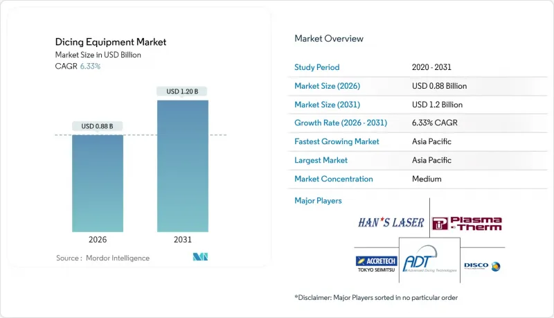
這項穩步擴張得益於半導體後端製造領域的強勁投資,尤其是在薄晶圓、先進封裝技術和寬能能隙功率裝置方面。在電動車、可再生能源和人工智慧工作負載日益成長的需求驅動下,晶片製造商優先考慮高產量比率晶粒分割,強調具有亞微米定位精度、污染控制製造流程和整合檢測能力的系統。向3D和異構整合的持續轉型推動了對等離子和雷射切割設備的需求,這些設備能夠最大限度地減少晶片碎裂並實現更窄的切割路徑。同時,不斷提高的自動化能力正在幫助晶圓廠解決勞動力短缺問題,縮短製程切換時間,並提高整體設備效率(OEE)。美國、歐洲和東亞的供應鏈區域化計畫正在催生新的區域需求中心,但由於稀土元素雷射光源的持續地緣政治摩擦以及對漿料處理的嚴格監管,資本密集度仍然很高。
全球切丁設備市場趨勢與洞察
精密運動系統的技術進步
運動控制技術的最新創新實現了亞微米級平台精度,這對於異質整合生產線至關重要。例如,DISCO 的 DFD6370 平台採用選購高度感測器,在加工 330 x 330 mm基板時,可將切割深度保持在 ±1 μm 以內,從而在面板級封裝中發揮優勢。主動阻尼、封閉回路型機器人控制和視覺引導對準進一步降低了振動和熱漂移,提高了加工易碎碳化矽晶圓的產量比率。整合多軸平台和板載計量功能的供應商提供承包定序單元,將切割、清洗和檢測整合在一個流程中,從而減少缺陷處理和縮短週期時間。
先進邏輯和記憶體工廠的需求迅速成長
根據SEMI的預測,2025年至2027年間,300毫米晶圓廠的總資本支出將達到4,000億美元,其中晶圓代工廠的支出將佔2,300億美元。新型極紫外線(EUV)製程節點和3D堆疊式DRAM生產線的引入增加了背面污染的風險,迫使晶圓廠採用具備靜電抑制和密封晶片修復功能的切割設備。隨著台積電、三星以及中國本土晶圓代工廠加速產能擴張,快速的設備交付和更完善的現場服務網路正成為設備供應商的關鍵採購標準。
加強對泥漿和化學廢棄物的監管
修訂後的 ISO 14644 無塵室標準和新的 PFAS 法規要求晶圓廠維修污水循環系統、安裝除氟系統並採用閉合迴路冷卻系統。在切割單元中整合回收模組和即時顆粒監測器的供應商正在幫助客戶降低營運成本,同時滿足監管標準。然而,額外的資本投入和設施維修在某些情況下會延緩採購決策。
細分市場分析
到2025年,刀片切割系統將佔據46.10%的切割設備市場佔有率,這得益於其晶圓單片成本優勢和成熟的服務網路,使其非常適合大批量邏輯和記憶體生產線。然而,隨著50µm以下晶圓的日益普及,由於對無縫單片定序的需求(傳統刀片切割無法保證這一點),雷射切割領域將以6.53%的複合年成長率成長。PanasonicAPX300等離子切割平台在300mm晶圓上實現了20µm的切割寬度,展現了等離子切割和雷射切割工具在性能上的飛躍。結合刀片粗切和雷射精加工的混合生產線也越來越受歡迎,實現了產能和晶粒強度之間的平衡。
雷射光學元件、稀土元素對準組件和多千瓦電源的額外成本仍然限制了價格敏感型晶圓廠對這些技術的採用。然而,在晶粒到封裝垂直互連和脆性碳化矽基板已成為主流的領域,較高的初始投資將被更低的廢品率和更嚴格的設計規則所抵消。在預測期內,超快脈衝整形技術和自動聚焦光學元件的持續研發可望提高設備運轉率,並逐步縮小單位晶圓成本差距。
半導體產業正向更大尺寸的晶圓轉型,預計到2031年,450毫米以上晶圓的複合年成長率將達到6.38%,接近300毫米晶圓的市佔率(2025年300毫米晶圓的市佔率為37.55%)。先進封裝應用,尤其是面板級封裝工藝,正在推動對更大尺寸基板加工能力的需求。 DISCO公司的DFD6370可加工最大尺寸為330x330毫米的工件,彌合了傳統晶圓加工與新興大尺寸需求之間的差距。
200mm以下的小尺寸晶圓對於MEMS元件和功率半導體等特殊應用仍然至關重要。成熟的晶圓尺寸規格在基板成本和製程最佳化方面具有優勢。 200mm晶圓市場受益於成熟的製程節點擴展和汽車半導體市場的需求,而150mm晶圓則服務於化合物半導體和傳統裝置生產等特定應用領域。然而,更大尺寸晶圓的經濟優勢,例如更高的晶粒基板產量比率和更低的單位加工成本,正在推動晶圓尺寸的轉變。 SEMI的《全球晶圓廠預測》指出,預計到2027年將有79個高機率晶圓廠投入運營,其中許多晶圓廠具備混合尺寸晶圓的生產能力。能夠開發擴充性處理系統,在單一平台上相容於多種晶圓尺寸的設備製造商,將更有利於應對這個不斷變化的市場環境。
區域分析
亞太地區憑藉著台灣、韓國、日本和中國當地等製造群的強大支撐,預計到2025年將維持42.55%的切割設備市場佔有率。東京政府提供的總額達3.9兆日圓(約260億美元)的補貼正在支持日本經濟復甦,訂單了精密運動控制供應商和自動化整合商的訂單成長。中國外包組裝服務(OSAT)企業正在加速部署等離子切割生產線,以提高其自主研發的人工智慧加速器的產量比率。同時,東南亞國家組裝業務的輻射效應也催生了對中型刀片切割機的需求。
北美《晶片製造和加工服務法案》(CHIPS Act)已提供超過500億美元的激勵資金,用於將亞利桑那州、德克薩斯州和紐約州北部的工廠從2026年起轉型為新的採購中心。這些工廠優先安裝全自動刀片和雷射切割單元,並配備預測性維護分析系統,以解決技術純熟勞工短缺問題。
歐洲晶片法案正向歐洲大陸的產能注入470億美元,其中德國和法國的計劃在主導。儘管產量仍落後於亞洲,但歐盟晶圓廠嚴格的環保標準正在加速封閉回路型漿料和低耗水等離子切割系統的應用,從而推高了該地區的平均售價。
其他福利:
- Excel格式的市場預測(ME)表
- 3個月的分析師支持
目錄
第1章 引言
- 研究假設和市場定義
- 調查範圍
第2章調查方法
第3章執行摘要
第4章 市場情勢
- 市場概覽
- 市場促進因素
- 精密運動系統的技術進步
- 先進邏輯和記憶體代工廠的需求激增
- 3D封裝和異質整合技術的快速普及
- 擴大電動車和可再生能源動力設備的應用
- 向等離子體切割技術過渡到超薄晶圓
- 中國獎勵
- 市場限制
- 高額資本投入和較長的投資回收期
- 因缺口和微裂紋造成的產量比率損失
- 加強對泥漿和化學品處置的監管
- 雷射光源供應瓶頸和稀土元素依賴性
- 宏觀經濟因素如何影響市場
- 產業供應鏈分析
- 監管環境
- 技術展望
- 波特五力分析
- 新進入者的威脅
- 買方和消費者的議價能力
- 供應商的議價能力
- 替代品的威脅
- 競爭對手之間的競爭
第5章 市場規模與成長預測
- 按技術領域
- 刀切
- 雷射消熔
- 隱密骰子
- 等離子切割
- 按晶圓尺寸
- 150毫米或更小
- 200 mm
- 300 mm
- 450毫米或以上
- 透過使用
- 邏輯與記憶體
- MEMS元件
- 功率元件
- CMOS影像感測器
- RFID/智慧卡
- 按最終用戶行業分類
- 晶圓代工廠
- IDM
- OSAT
- 按地區
- 北美洲
- 美國
- 加拿大
- 墨西哥
- 南美洲
- 巴西
- 阿根廷
- 南美洲其他地區
- 歐洲
- 德國
- 英國
- 法國
- 義大利
- 西班牙
- 俄羅斯
- 其他歐洲地區
- 亞太地區
- 中國
- 日本
- 印度
- 韓國
- 東南亞
- 亞太其他地區
- 中東和非洲
- 中東
- 沙烏地阿拉伯
- 阿拉伯聯合大公國
- 其他中東地區
- 非洲
- 南非
- 埃及
- 其他非洲地區
- 中東
- 北美洲
第6章 競爭情勢
- 市場集中度
- 策略趨勢
- 市佔率分析
- 公司簡介
- DISCO Corporation
- Tokyo Seimitsu Co., Ltd.(ACCRETECH)
- Advanced Dicing Technologies Ltd.
- Panasonic Connect Co., Ltd.
- SPTS Technologies Ltd.(KLA Corporation)
- Plasma-Therm LLC
- Veeco Instruments Inc.
- Synova SA
- 3D-Micromac AG
- Han's Laser Technology Industry Group Co., Ltd.
- Suzhou Delphi Laser Co., Ltd.
- EO Technics Co., Ltd.
- Neon Tech Co., Ltd.
- ASM Laser Separation International BV
- Kulicke & Soffa Industries, Inc.
- Takatori Corporation
- Lumentum Holdings Inc.(dicing lasers)
- IPG Photonics Corporation
- Oxford Instruments Plasma Technology
- Plasma Etch Inc.
- Dynatex International
- Loadpoint Micro Machining Ltd.
- Disco Hi-Tec America, Inc.
- Shenzhen JLH Laser Co., Ltd.
- Wuhan HGLaser Engineering Co., Ltd.
第7章 市場機會與未來展望
Dicing equipment market size in 2026 is estimated at USD 0.88 billion, growing from 2025 value of USD 0.83 billion with 2031 projections showing USD 1.2 billion, growing at 6.33% CAGR over 2026-2031.
Robust investment in semiconductor backend manufacturing, especially for thinner wafers, advanced packaging formats, and wide-bandgap power devices, underpins this steady expansion. As electric-vehicle, renewable-energy, and AI workloads intensify, chipmakers prioritize high-yield die singulation, favoring systems that combine sub-micrometer positioning accuracy, contamination-controlled processing, and integrated inspection. Continuous migration toward 3D and heterogeneous integration is elevating the demand for plasma and laser dicing tools that minimize chipping and enable narrower streets. Meanwhile, automation upgrades help fabs offset labor constraints, shorten changeover times, and boost overall equipment effectiveness. Supply-chain localization programs in the United States, Europe, and East Asia introduce new regional demand nodes; however, persistent geopolitical frictions surrounding rare-earth laser sources and stringent slurry-disposal rules continue to keep capital intensity high.
Global Dicing Equipment Market Trends and Insights
Technological Advancements in High-Precision Motion Systems
Recent motion-control breakthroughs deliver sub-micrometer stage accuracy essential for heterogeneous integration lines. DISCO's DFD6370 platform, for instance, handles 330 X 330 mm substrates while using selectable height sensors that keep cut depth within +-1 µm, an advantage for panel-level packaging. Active damping, closed-loop robotics, and vision-guided alignment further trim vibration and thermal drift, enabling higher yield when processing brittle silicon-carbide wafers. Vendors integrating multi-axis stages with on-board metrology now offer turnkey singulation cells that combine cutting, cleaning, and inspection in a single flow, reducing handling defects and cycle time.
Surge in Demand from Advanced Logic and Memory Fabs
SEMI projects cumulative 300 mm fab equipment outlays to reach USD 400 billion between 2025 and 2027, with foundries accounting for USD 230 billion of that total. New extreme-ultraviolet nodes and 3D-stacked DRAM lines magnify backside contamination risks, prompting fabs to specify dicing tools with electrostatic-charge suppression and hermetic chip-collection. As capacity ramps accelerate, particularly at TSMC, Samsung, and China's domestic foundries, rapid tool delivery and field-service reach become procurement gatekeepers for equipment suppliers.
Stricter Slurry/Chemical Disposal Regulations
ISO 14644 cleanroom revisions and emerging PFAS controls require fabs to retrofit wastewater loops, install fluorinated-compound abatement systems, and adopt closed-loop coolants.Vendors that embed recycling modules and real-time particulate monitors inside dicing cells help customers meet regulatory thresholds while reducing utility bills; however, the added equipment cost and facility retrofit delay some purchase decisions.
Other drivers and restraints analyzed in the detailed report include:
- Rapid Adoption of 3D Packaging and Heterogeneous Integration
- Growing Deployment of Power Devices for EV and Renewables
- Laser Source Supply Bottlenecks and Rare-Earth Dependency
For complete list of drivers and restraints, kindly check the Table Of Contents.
Segment Analysis
Blade systems controlled 46.10% of the dicing equipment market in 2025, their cost-per-wafer edge and mature service networks suiting high-volume logic and memory lines. However, the laser segment is expanding at a 6.53% CAGR as sub-50 µm wafers proliferate, requiring kerf-free singulation that conventional blades cannot guarantee. Panasonic's APX300 plasma platform enables 20 µm streets on 300 mm wafers, underscoring the performance leap plasma and laser tools deliver. Hybrid lines that combine blade rough-cutting with laser finishing are also gaining traction, striking a balance between throughput and die strength.
The incremental cost of laser optics, rare-earth alignment components, and multi-kW power supplies still limits adoption in price-sensitive fabs. Yet where die-to-package vertical interconnect or brittle SiC substrates prevail, the higher upfront spend is offset by lower scrap and tighter design rules. Over the forecast horizon, sustained research and development in ultrafast pulse shaping and auto-focus optics is expected to enhance tool duty cycle, gradually narrowing the per-wafer cost gap.
The semiconductor industry is transitioning to larger wafer formats, with wafers exceeding 450 mm projected to grow at a 6.38% CAGR through 2031, challenging the 300 mm wafers, which held a 37.55% market share in 2025. Advanced packaging applications, particularly in panel-level packaging workflows, are driving demand for larger substrate-handling capabilities. DISCO Corporation's DFD6370 supports workpieces up to 330 X 330 mm, addressing the gap between conventional wafer processing and emerging large-format requirements.
Smaller wafer sizes, including 200 mm and below, remain relevant in specialized applications such as MEMS devices and power semiconductors, where substrate costs and process optimization favor established formats. The 200 mm segment benefits from mature node expansion and automotive semiconductor demand, while 150 mm wafers serve niche applications in compound semiconductors and legacy device production. However, the economic advantages of larger wafers, including higher die yield per substrate and reduced per-unit processing costs, are driving format migration. SEMI's World Fab Forecast identifies 79 high-probability facilities beginning operations through 2027, many incorporating mixed wafer-size capabilities. Equipment suppliers developing scalable handling systems for multiple wafer formats within single platforms are well-positioned for this evolving landscape.
The Dicing Equipment Market Report is Segmented by Dicing Technology (Blade Dicing, Laser Ablation, Stealth Dicing, and More), Wafer Size (<= 150 Mm, 200 Mm, 300 Mm, and More) Application (Logic and Memory, MEMS Devices, Power Devices, CMOS Image Sensors, and More), End-User Industry (Foundries, Idms, and OSATs) and Geography (North America, Europe, Asia-Pacific, and More). The Market Forecasts are Provided in Terms of Value (USD).
Geography Analysis
The Asia-Pacific region retained a 42.55% share of the dicing equipment market in 2025, driven by its deep-seated manufacturing clusters across Taiwan, South Korea, Japan, and mainland China. Tokyo-backed subsidies totaling JPY 3.9 trillion (USD 0.026 trillion) underpin Japan's resurgence, channeling orders to precision-motion vendors and automation integrators. Chinese OSATs accelerate plasma-dicing line installs to raise yields on locally designed AI accelerators, while Southeast Asian nations attract assembly spillover, spawning mid-tier blade-dicer demand.
North America's CHIPS Act has unlocked more than USD 50 billion in incentives, transforming greenfield fabs in Arizona, Texas, and upstate New York into new procurement hubs starting in 2026. These sites prioritize fully automated blade and laser cells, equipped with predictive maintenance analytics, to offset skilled labor shortages.
Europe's Chips Act funnels USD 47 billion into continental capacity, led by German and French projects focused on silicon-carbide power electronics for EV supply chains. Although smaller than Asian volumes, the stringent environmental standards in EU fabs accelerate uptake of closed-loop slurry and low-water-consumption plasma dicing systems, nudging regional ASPs upward.
- DISCO Corporation
- Tokyo Seimitsu Co., Ltd. (ACCRETECH)
- Advanced Dicing Technologies Ltd.
- Panasonic Connect Co., Ltd.
- SPTS Technologies Ltd. (KLA Corporation)
- Plasma-Therm LLC
- Veeco Instruments Inc.
- Synova SA
- 3D-Micromac AG
- Han's Laser Technology Industry Group Co., Ltd.
- Suzhou Delphi Laser Co., Ltd.
- EO Technics Co., Ltd.
- Neon Tech Co., Ltd.
- ASM Laser Separation International B.V.
- Kulicke & Soffa Industries, Inc.
- Takatori Corporation
- Lumentum Holdings Inc. (dicing lasers)
- IPG Photonics Corporation
- Oxford Instruments Plasma Technology
- Plasma Etch Inc.
- Dynatex International
- Loadpoint Micro Machining Ltd.
- Disco Hi-Tec America, Inc.
- Shenzhen JLH Laser Co., Ltd.
- Wuhan HGLaser Engineering Co., Ltd.
Additional Benefits:
- The market estimate (ME) sheet in Excel format
- 3 months of analyst support
TABLE OF CONTENTS
1 INTRODUCTION
- 1.1 Study Assumptions and Market Definition
- 1.2 Scope of the Study
2 RESEARCH METHODOLOGY
3 EXECUTIVE SUMMARY
4 MARKET LANDSCAPE
- 4.1 Market Overview
- 4.2 Market Drivers
- 4.2.1 Technological advancements in high-precision motion systems
- 4.2.2 Surge in demand from advanced logic and memory fabs
- 4.2.3 Rapid adoption of 3D packaging and heterogeneous integration
- 4.2.4 Growing deployment of power devices for EV and renewables
- 4.2.5 Shift toward plasma dicing for ultra-thin wafers
- 4.2.6 Localization incentives for domestic equipment in China
- 4.3 Market Restraints
- 4.3.1 High capital expenditure and long pay-back period
- 4.3.2 Yield losses from chipping and micro-cracks
- 4.3.3 Stricter slurry/chemical disposal regulations
- 4.3.4 Laser source supply bottlenecks and rare-earth dependency
- 4.4 Impact of Macroeconomic Factors on the Market
- 4.5 Industry Supply Chain Analysis
- 4.6 Regulatory Landscape
- 4.7 Technological Outlook
- 4.8 Porter's Five Forces Analysis
- 4.8.1 Threat of New Entrants
- 4.8.2 Bargaining Power of Buyers/Consumers
- 4.8.3 Bargaining Power of Suppliers
- 4.8.4 Threat of Substitute Products
- 4.8.5 Intensity of Competitive Rivalry
5 MARKET SIZE AND GROWTH FORECASTS (VALUE)
- 5.1 By Dicing Technology
- 5.1.1 Blade Dicing
- 5.1.2 Laser Ablation
- 5.1.3 Stealth Dicing
- 5.1.4 Plasma Dicing
- 5.2 By Wafer Size
- 5.2.1 <= 150 mm
- 5.2.2 200 mm
- 5.2.3 300 mm
- 5.2.4 >= 450 mm
- 5.3 By Application
- 5.3.1 Logic and Memory
- 5.3.2 MEMS Devices
- 5.3.3 Power Devices
- 5.3.4 CMOS Image Sensors
- 5.3.5 RFID / Smart Cards
- 5.4 By End-User Industry
- 5.4.1 Foundries
- 5.4.2 IDMs
- 5.4.3 OSATs
- 5.5 By Geography
- 5.5.1 North America
- 5.5.1.1 United States
- 5.5.1.2 Canada
- 5.5.1.3 Mexico
- 5.5.2 South America
- 5.5.2.1 Brazil
- 5.5.2.2 Argentina
- 5.5.2.3 Rest of South America
- 5.5.3 Europe
- 5.5.3.1 Germany
- 5.5.3.2 United Kingdom
- 5.5.3.3 France
- 5.5.3.4 Italy
- 5.5.3.5 Spain
- 5.5.3.6 Russia
- 5.5.3.7 Rest of Europe
- 5.5.4 Asia-Pacific
- 5.5.4.1 China
- 5.5.4.2 Japan
- 5.5.4.3 India
- 5.5.4.4 South Korea
- 5.5.4.5 South-East Asia
- 5.5.4.6 Rest of Asia-Pacific
- 5.5.5 Middle East and Africa
- 5.5.5.1 Middle East
- 5.5.5.1.1 Saudi Arabia
- 5.5.5.1.2 United Arab Emirates
- 5.5.5.1.3 Rest of Middle East
- 5.5.5.2 Africa
- 5.5.5.2.1 South Africa
- 5.5.5.2.2 Egypt
- 5.5.5.2.3 Rest of Africa
- 5.5.5.1 Middle East
- 5.5.1 North America
6 COMPETITIVE LANDSCAPE
- 6.1 Market Concentration
- 6.2 Strategic Moves
- 6.3 Market Share Analysis
- 6.4 Company Profiles (includes Global level Overview, Market level overview, Core Segments, Financials as available, Strategic Information, Market Rank/Share for key companies, Products and Services, and Recent Developments)
- 6.4.1 DISCO Corporation
- 6.4.2 Tokyo Seimitsu Co., Ltd. (ACCRETECH)
- 6.4.3 Advanced Dicing Technologies Ltd.
- 6.4.4 Panasonic Connect Co., Ltd.
- 6.4.5 SPTS Technologies Ltd. (KLA Corporation)
- 6.4.6 Plasma-Therm LLC
- 6.4.7 Veeco Instruments Inc.
- 6.4.8 Synova SA
- 6.4.9 3D-Micromac AG
- 6.4.10 Han's Laser Technology Industry Group Co., Ltd.
- 6.4.11 Suzhou Delphi Laser Co., Ltd.
- 6.4.12 EO Technics Co., Ltd.
- 6.4.13 Neon Tech Co., Ltd.
- 6.4.14 ASM Laser Separation International B.V.
- 6.4.15 Kulicke & Soffa Industries, Inc.
- 6.4.16 Takatori Corporation
- 6.4.17 Lumentum Holdings Inc. (dicing lasers)
- 6.4.18 IPG Photonics Corporation
- 6.4.19 Oxford Instruments Plasma Technology
- 6.4.20 Plasma Etch Inc.
- 6.4.21 Dynatex International
- 6.4.22 Loadpoint Micro Machining Ltd.
- 6.4.23 Disco Hi-Tec America, Inc.
- 6.4.24 Shenzhen JLH Laser Co., Ltd.
- 6.4.25 Wuhan HGLaser Engineering Co., Ltd.
7 MARKET OPPORTUNITIES AND FUTURE OUTLOOK
- 7.1 White-space and Unmet-Need Assessment
