


 |
市場調查報告書
商品編碼
1939711
半導體蝕刻設備:市場佔有率分析、產業趨勢與統計、成長預測(2026-2031)Semiconductor Etch Equipment - Market Share Analysis, Industry Trends & Statistics, Growth Forecasts (2026 - 2031) |
||||||
※ 本網頁內容可能與最新版本有所差異。詳細情況請與我們聯繫。
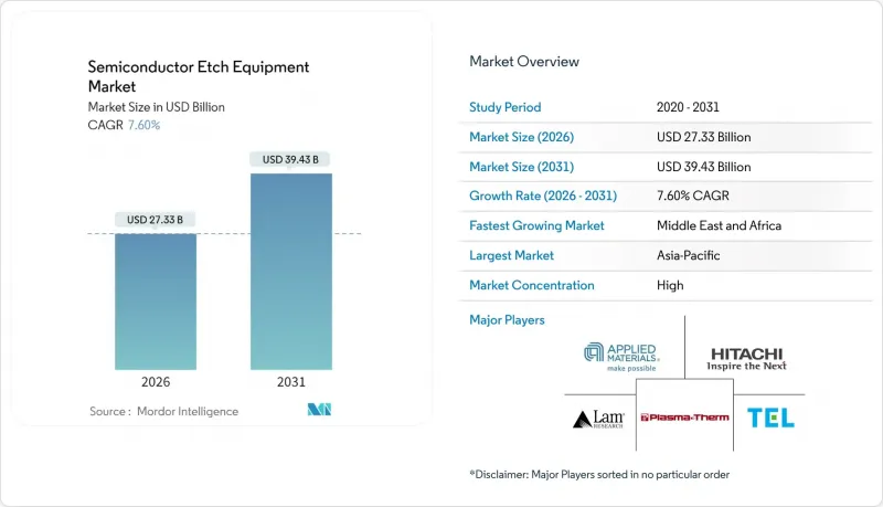
預計半導體蝕刻設備市場將從 2025 年的 254 億美元成長到 2026 年的 273.3 億美元,到 2031 年將達到 394.3 億美元,2026 年至 2031 年的複合年成長率為 7.60%。
這一成長反映了對先進製程節點的持續資本投資、環柵電晶體的加速普及以及異質整合技術的廣泛部署。人工智慧工作負載的不斷成長、電動車產量的擴大以及政府補貼計劃持續擴大已安裝設備的潛在市場規模,而持續的氦氣短缺和出口管制限制則影響著投資時機。儘管邏輯和微處理器代工廠仍然是設備需求量最大的客戶,佔據了最大的出貨量佔有率,但隨著資料中心營運商對更高頻寬和更高能源效率的需求,高頻寬記憶體和先進封裝生產線的出貨量成長最為迅速。雖然原子層蝕刻平台的收入成長最為顯著,但由於其高吞吐量和化學柔軟性,感應耦合電漿設備仍然是高產量生產線的基礎。從區域來看,亞太地區在裝置容量佔據主導地位,但受北美、歐洲和中東地區政府補貼支持的晶圓廠計劃的推動,半導體蝕刻設備市場的地理分佈正在穩步多元化。
全球半導體蝕刻設備市場趨勢及展望
元件小型化至3nm節點以下
隨著邏輯電路特徵尺寸的不斷縮小,晶圓廠越來越依賴能夠實現原子級尺寸控制並最大限度減少等離子體損傷的蝕刻系統。三星3nm環柵元件的量產和台積電N2製程的認證,正推動著對逐層去除材料的原子層蝕刻腔的即時需求。應用材料公司和Lam Research憑藉其專有的脈衝等離子體循環和不飽和技術,實現了亞奈米級的尺寸偏差控制,這增強了它們的競爭優勢,而小規模的供應商則難以獲得同等的研發資金。英特爾的18A藍圖對尺寸控制提出了更高的要求,這鞏固了未來幾年對支援這些節點的供應商的需求預測。隨著節點轉換導致薄膜堆疊層數增加,包括高介電常數材料和釕隔離層,差異化的化學處理技術進一步推高了晶圓廠的轉換成本,並增強了主要設備製造商的定價能力。
中國鑄造廠產能快速擴張
儘管整個產業成長放緩,但預計到2024年,中國邏輯晶片和特種晶圓代工廠每月仍將新增約20萬片晶圓,約佔全球新增產能的15%。政府注資和優惠的土地租賃條款正在加速新晶圓廠的建設,而出口許可證的不確定性則迫使營運商加快設備交付。雖然像Naura這樣的國內領先製造商正在提高其在中節點蝕刻設備領域的供應佔有率,但先進節點的大部分訂單仍然流向了國外頂級供應商。為因應監管變化而進行的庫存儲備,即使在整個行業增速放緩的情況下,也維持了較高的季度訂單量,從而減輕了半導體蝕刻設備市場在典型景氣衰退中受到的影響。
記憶體產業資本投資的週期性波動
為了應對產能過剩,記憶體製造商通常會削減資本支出預算。 SK海力士、美光和三星在2024年初削減了約25%的蝕刻設備採購,並減少了季度設備出貨量,以應對供應過剩。由於3D NAND堆疊需要超過200道蝕刻工序,因此支出暫停對蝕刻設備供應商的收入影響尤其顯著。儘管邏輯裝置產業的波動在一定程度上抵消了記憶體產業的影響,但記憶體週期的波動仍然會導致供應商生產計畫的波動。
細分市場分析
到2025年,邏輯和微處理器晶圓廠將佔據半導體蝕刻設備市場36.65%的佔有率,憑藉其向3奈米以下製程尺寸快速過渡的優勢,繼續保持領先地位。每個新的製程節點都需要更精確的輪廓控制,增加了每片晶圓的蝕刻成本。智慧型手機和資料中心的持續更新換代推動了晶圓生產,而用於自動駕駛的混合訊號晶片也貢獻了額外的產量。儘管記憶體容量的成長仍然不穩定,但超過230層的3D NAND快閃記憶體正在持續推動對深溝槽蝕刻的需求。預計到2031年,先進封裝和高頻寬記憶體生產線將以8.79%的複合年成長率成長,這得益於將邏輯晶粒與堆疊式DRAM相結合的AI加速器需求的成長。
隨著無晶圓廠半導體製造商尋求風險分擔模式,代工服務日益受到重視。台積電預計2025年底,其CoWoS月產能將擴大至6.5萬片晶圓。隨著碳化矽開關在電動車逆變器和快速充電器的應用日益廣泛,對功率元件和分立元件的需求也在加速成長,這需要專門的深反應離子刻蝕系統。微機電系統(MEMS)和感測器製造商正在利用低壓等離子體模組製造麥克風陣列和胎壓監測器。新興的光子裝置和量子裝置目前仍屬於小眾市場,但它們對原子級蝕刻選擇性的需求正在為供應商差異化開闢新的途徑。
2025年,感應耦合電漿)設備將佔總收入的33.25%,鞏固其作為大批量晶圓廠核心設備的地位。其廣泛的化學處理能力使得單一平台即可處理多晶矽、高介電常數材料和金屬閘極,簡化了生產線維護。反應離子蝕刻(RIE)設備在後續製程節點中持續被應用,這些節點對長寬比更為寬鬆。深RIE設備則憑藉其獨特的優勢,在微機電系統(MEMS)和矽通孔(TSV)等專業領域佔據主導地位,並維持著較高的利潤率。
隨著半導體蝕刻設備市場向埃級精度控制轉型,原子層蝕刻平台以9.01%的複合年成長率實現了最高成長。應用材料公司大力推廣一種脈衝射頻刻蝕工藝,該工藝每個循環可去除單分子層。高長寬比模組可解決縱橫比超過60:1的3D NAND溝槽問題,避免側壁彎曲導致的單元效率下降。濕式蝕刻系統仍用於等向性清洗和預鍵合表面處理,但隨著等離子體化學製程變得更加溫和、更具選擇性,其市佔率正在下降。
區域分析
到2025年,亞太地區將佔全球營收的70.85%,其中台灣、韓國和中國當地將繼續新增數十億美元的產能。台積電的CoWoS(CoWoS)產能擴張至每月6.5萬片,彰顯了該地區在先進封裝領域的主導;三星和SK海力士的DRAM和NAND閃存週期持續推動著大規模的蝕刻需求。中國本土廠商正快速提昇技術水平,NAURA 44%的利潤成長以及躋身全球前六強便是最好的證明。
北美地區的市佔率得益於《晶片技術創新法案》(CHIPS Act)提供的超過500億美元的激勵資金。英特爾在俄亥俄州投資200億美元的建設計劃以及台積電在亞利桑那州的工廠,正在推動大型多腔蝕刻設備的訂單成長,使供應商的訂單不再那麼依賴亞洲。歐洲的《晶片技術創新法案》資金則推動了德國、法國和愛爾蘭的計劃,使設備出貨前景得以延續至2020年代末期。
受各國政府追求戰略自主的推動,中東和非洲地區預計將實現最高的複合年成長率(CAGR),達到10.74%。沙烏地阿拉伯NEOM園區和阿拉伯聯合大公國的無塵室計畫建造試點生產線,以部署承包蝕刻模組。儘管基礎設施和人才短缺仍然是挑戰,但持續的公共資金投入正在吸引全球供應商,進一步擴大半導體蝕刻設備市場的地域覆蓋範圍。
其他福利:
- Excel格式的市場預測(ME)表
- 3個月的分析師支持
目錄
第1章 引言
- 研究假設和市場定義
- 調查範圍
第2章調查方法
第3章執行摘要
第4章 市場情勢
- 市場概覽
- 宏觀經濟因素的影響
- 產業供應鏈分析
- 市場促進因素
- 元件小型化至3nm節點以下
- 中國鑄造廠產能快速擴張
- 向全環柵極(GAA)電晶體過渡
- 功率元件領域對從 300 毫米到 200 毫米的改造需求
- 美國和歐盟晶圓廠補貼支出(晶片法案)
- 異質整合和先進封裝
- 市場限制
- 記憶體產業資本投資的週期性波動
- 氦氣和稀有氣體供應中斷
- 設備平均售價上漲與投資收益(ROI) 的關係
- 出口管制合規成本增加
- 監管環境
- 技術展望
- 波特五力分析
- 新進入者的威脅
- 買方和消費者的議價能力
- 供應商的議價能力
- 替代品的威脅
- 競爭對手之間的競爭
第5章 市場規模與成長預測
- 透過使用
- 邏輯/微處理器
- 記憶
- 鑄造服務
- 功率元件和分立元件
- 微機電系統和感測器
- 先進封裝/HBM
- 其他
- 透過裝置
- 反應離子蝕刻設備(RIE)
- 感應耦合電漿(ICP)蝕刻設備
- 深反應電離(DRIE)
- 濕蝕刻系統
- 高長寬比蝕刻(HARP)
- 原子層蝕刻(ALE)
- 透過蝕刻技術
- 乾蝕刻
- 濕蝕刻
- 透過流程
- 前端製程 (FEOL) 蝕刻
- 後端製程 (BEOL) 蝕刻
- 地區
- 北美洲
- 美國
- 加拿大
- 墨西哥
- 南美洲
- 巴西
- 阿根廷
- 南美洲其他地區
- 歐洲
- 德國
- 英國
- 法國
- 義大利
- 西班牙
- 俄羅斯
- 其他歐洲地區
- 亞太地區
- 中國
- 日本
- 印度
- 韓國
- 東南亞
- 亞太其他地區
- 中東和非洲
- 中東
- 沙烏地阿拉伯
- 阿拉伯聯合大公國
- 土耳其
- 其他中東地區
- 非洲
- 南非
- 奈及利亞
- 其他非洲地區
- 中東
- 北美洲
第6章 競爭情勢
- 市場集中度
- 策略趨勢
- 市佔率分析
- 公司簡介
- Applied Materials, Inc.
- Lam Research Corp.
- Tokyo Electron Ltd.
- Hitachi High-Tech Corp.
- Plasma-Therm LLC
- ASM International NV
- NAURA Technology Group Co., Ltd.
- Oxford Instruments Plasma Technology Ltd.
- SPTS Technologies Ltd.(KLA)
- ULVAC, Inc.
- Veeco Instruments Inc.
- SAMCO Inc.
- Advanced Micro-Fabrication Equipment Inc.(AMEC)
- Mattson Technology Inc.
- GlobalFoundries Inc.(In-house Tools)
- Suzhou Ruidow Technology Co., Ltd.
- PVA TePla AG
- CORIAL SAS
- Trion Technology Inc.
- Tescan Orsay Holding as
第7章 市場機會與未來展望
The semiconductor etch equipment market is expected to grow from USD 25.4 billion in 2025 to USD 27.33 billion in 2026 and is forecast to reach USD 39.43 billion by 2031 at 7.60% CAGR over 2026-2031.
This growth reflects sustained capital spending at advanced process nodes, accelerating adoption of gate-all-around transistors, and wider deployment of heterogeneous integration. Rising artificial-intelligence workloads, expanding electric-vehicle production, and national subsidy programs continue to enlarge the addressable base of installed tools, while persistent helium shortages and export-control rules shape investment timing. Logic and microprocessor fabs remain the most equipment-intensive customers, commanding the largest share of shipments, yet high-bandwidth-memory and advanced-packaging lines post the fastest unit growth as data-center operators require higher bandwidth and improved energy efficiency. Atomic-layer-etch platforms record the highest revenue momentum, but inductively coupled plasma tools still anchor high-volume manufacturing lines because of their throughput and chemistry flexibility. Regionally, Asia-Pacific dominates installed capacity, although subsidy-backed fab projects in North America, Europe, and the Middle East steadily diversify the geographic footprint of the semiconductor etch equipment market.
Global Semiconductor Etch Equipment Market Trends and Insights
Equipment miniaturization below 3 nm node
Shrinking logic geometries compel fabs to adopt etchers that deliver atomic-level dimensional control while limiting plasma-induced damage. Samsung's volume ramp of 3 nm gate-all-around devices and TSMC's N2 process qualification amplify immediate demand for atomic-layer-etch chambers that remove material one monolayer at a time. Applied Materials and Lam Research deploy proprietary pulsed-plasma cycles and in-situ metrology to meet sub-nanometer variability budgets, which strengthens their competitive moat as smaller vendors struggle to fund similar R&D. Intel's 18A roadmap extends the requirement for even tighter profile control, anchoring multi-year visibility for suppliers positioned on these nodes. As node migration pushes film stacks toward high-k dielectrics and ruthenium barriers, differentiated chemistries further raise switching costs for fabs and reinforce pricing power for leading toolmakers.
Rapid capacity build in Chinese foundries
Chinese logic and specialty foundries added roughly 200,000 wafer starts per month in 2024, equal to nearly 15% of global build-out, despite broader cyclical softness. Government equity injections and advantageous land leasing accelerate greenfield construction, while export-license uncertainty prompts operators to front-load equipment receipts. Domestic champions such as NAURA supply an expanding share of mid-node etchers, but tier-one foreign vendors still capture most advanced-node orders. Stockpiling ahead of anticipated rule changes keeps quarterly bookings elevated even during industry pauses, cushioning the semiconductor etch equipment market against typical downturns.
Cyclical cap-ex swings in memory sector
Memory producers periodically slash equipment budgets to correct overcapacity. SK Hynix, Micron, and Samsung cut etch purchases by nearly 25% in early 2024 following a supply glut, dampening quarterly tool shipments. Because 3D NAND stacks require more than 200 etch passes, each spending pause disproportionately weights the revenue of etch suppliers. Although the logic segment provides a partial offset, the amplitude of memory cycles injects volatility into production planning for equipment vendors.
Other drivers and restraints analyzed in the detailed report include:
- Transition to gate-all-around transistors
- 300 mm-to-200 mm retrofit demand in power devices
- Helium and rare-gas supply disruptions
For complete list of drivers and restraints, kindly check the Table Of Contents.
Segment Analysis
Logic and microprocessor fabs accounted for a 36.65% share of the semiconductor etch equipment market size in 2025, securing that primacy by migrating fastest toward sub-3 nm structures. Each new node requires tighter profile control, thereby boosting per-wafer etch spend. Continuous smartphone and data-center refresh cycles reinforce wafer starts, while mixed-signal chips for automotive autonomy add incremental volume. Memory capacity additions remain episodic, but 3D NAND layer counts above 230 sustain deep-trench etch demand. Advanced packaging and high-bandwidth-memory lines, projected to grow at an 8.79% CAGR through 2031, gain from AI accelerators that pair logic dies with stacked DRAM.
Foundry services attract fabless chipmakers seeking risk-sharing models, pushing TSMC to expand CoWoS packaging output to 65,000 wafers per month by late 2025. Power and discrete devices accelerate as electric-vehicle inverters and fast chargers embed more SiC switches, drawing specialized deep-reactive-ion systems. MEMS and sensor makers exploit low-pressure plasma modules for microphone arrays and tire-pressure monitors. Emerging photonic and quantum devices, though presently niche, demand atomic-level etch selectivity, offering new avenues for supplier differentiation.
Inductively coupled plasma tools delivered 33.25% of 2025 revenue, cementing their status as the backbone of high-volume fabs. Their broad chemistry range allows one platform to tackle polysilicon, high-k dielectrics, and metal gates, simplifying line maintenance. Reactive-ion systems retain service in trailing nodes where aspect-ratio constraints are modest. Deep-RIE tools capture specialty segments such as MEMS and through-silicon-vias, commanding premium margins for their niche capability.
Atomic-layer-etch platforms record the highest growth at a 9.01% CAGR as the semiconductor etch equipment market pivots toward angstrom-level control. Applied Materials advertises pulsed radio-frequency steps that remove a single monolayer per cycle. High-aspect-ratio modules tackle 3D NAND trenches exceeding 60:1, where sidewall bowing can cripple cell efficiency. Wet-bench systems persist for isotropic cleans and pre-bond surface prep, yet their total share erodes as plasma chemistries grow gentler and more selective.
The Semiconductor Etch Equipment Market Report is Segmented by Application (Logic/MPU, Memory, and More), Equipment Type (Reactive Ion Etcher, ICP Etcher, Deep RIE, Wet Etch Systems, High-Aspect-Ratio Etch, and Atomic Layer Etch), Etching Technology (Dry Etch and Wet Etch), Process Type (Front-End-Of-Line (FEOL) Etching and Back-End-Of-Line (BEOL) Etching), and Geography. The Market Forecasts are Provided in Terms of Value (USD).
Geography Analysis
Asia-Pacific generated 70.85% of 2025 revenue as Taiwan, South Korea, and mainland China sustained multi-billion-dollar capacity additions. TSMC's CoWoS expansion to 65,000 wafers per month illustrates regional leadership in advanced packaging, while Samsung and SK Hynix cycles in DRAM and NAND continue to command large etch volumes. Domestic Chinese vendors climb the learning curve rapidly; NAURA's 44% profit growth and move into the global top-six underlines this progress.
North America's share is buoyed by CHIPS Act incentives exceeding USD 50 billion. Intel's USD 20 billion Ohio build and TSMC's Arizona site pull large multi-chamber etch orders, diversifying supplier backlog away from sole reliance on Asia. European Chips Act funds steer projects in Germany, France, and Ireland, extending visibility for equipment shipments through decade-end.
The Middle East and Africa record the fastest projected CAGR at 10.74% as governments seek strategic autonomy. Saudi Arabia's NEOM campus and the United Arab Emirates' clean-room programs commit to pilot lines that import turnkey etch modules. Infrastructure gaps and talent shortages remain hurdles, yet sustained public funding attracts global suppliers, further widening the geographic base of the semiconductor etch equipment market.
- Applied Materials, Inc.
- Lam Research Corp.
- Tokyo Electron Ltd.
- Hitachi High-Tech Corp.
- Plasma-Therm LLC
- ASM International N.V.
- NAURA Technology Group Co., Ltd.
- Oxford Instruments Plasma Technology Ltd.
- SPTS Technologies Ltd. (KLA)
- ULVAC, Inc.
- Veeco Instruments Inc.
- SAMCO Inc.
- Advanced Micro-Fabrication Equipment Inc. (AMEC)
- Mattson Technology Inc.
- GlobalFoundries Inc. (In-house Tools)
- Suzhou Ruidow Technology Co., Ltd.
- PVA TePla AG
- CORIAL SAS
- Trion Technology Inc.
- Tescan Orsay Holding a.s.
Additional Benefits:
- The market estimate (ME) sheet in Excel format
- 3 months of analyst support
TABLE OF CONTENTS
1 INTRODUCTION
- 1.1 Study Assumptions and Market Definition
- 1.2 Scope of the Study
2 RESEARCH METHODOLOGY
3 EXECUTIVE SUMMARY
4 MARKET LANDSCAPE
- 4.1 Market Overview
- 4.2 Impact of Macroeconomic Factors
- 4.3 Industry Supply Chain Analysis
- 4.4 Market Drivers
- 4.4.1 Equipment miniaturization below 3 nm node
- 4.4.2 Rapid capacity-build in Chinese foundries
- 4.4.3 Transition to gate-all-around (GAA) transistors
- 4.4.4 300 mm-to-200 mm retrofit demand in power devices
- 4.4.5 U.S. and EU fab-subsidy outlays (CHIPS Acts)
- 4.4.6 Heterogeneous integration and advanced packaging
- 4.5 Market Restraints
- 4.5.1 Cyclical cap-ex swings in memory sector
- 4.5.2 Helium and rare-gas supply disruptions
- 4.5.3 Rising tool average selling prices vs ROI
- 4.5.4 Escalating export-control compliance costs
- 4.6 Regulatory Landscape
- 4.7 Technological Outlook
- 4.8 Porter's Five Forces Analysis
- 4.8.1 Threat of New Entrants
- 4.8.2 Bargaining Power of Buyers/Consumers
- 4.8.3 Bargaining Power of Suppliers
- 4.8.4 Threat of Substitute Products
- 4.8.5 Intensity of Competitive Rivalry
5 MARKET SIZE AND GROWTH FORECASTS (VALUE)
- 5.1 By Application
- 5.1.1 Logic / MPU
- 5.1.2 Memory
- 5.1.3 Foundry Services
- 5.1.4 Power and Discrete Devices
- 5.1.5 MEMS and Sensors
- 5.1.6 Advanced Packaging / HBM
- 5.1.7 Others
- 5.2 By Equipment Type
- 5.2.1 Reactive Ion Etcher (RIE)
- 5.2.2 Inductively Coupled Plasma (ICP) Etcher
- 5.2.3 Deep RIE (DRIE)
- 5.2.4 Wet Etch Systems
- 5.2.5 High-Aspect-Ratio Etch (HARP)
- 5.2.6 Atomic Layer Etch (ALE)
- 5.3 By Etching Technology
- 5.3.1 Dry Etch
- 5.3.2 Wet Etch
- 5.4 By Process Type
- 5.4.1 Front-End-of-Line (FEOL) Etching
- 5.4.2 Back-End-of-Line (BEOL) Etching
- 5.5 Geography
- 5.5.1 North America
- 5.5.1.1 United States
- 5.5.1.2 Canada
- 5.5.1.3 Mexico
- 5.5.2 South America
- 5.5.2.1 Brazil
- 5.5.2.2 Argentina
- 5.5.2.3 Rest of South America
- 5.5.3 Europe
- 5.5.3.1 Germany
- 5.5.3.2 United Kingdom
- 5.5.3.3 France
- 5.5.3.4 Italy
- 5.5.3.5 Spain
- 5.5.3.6 Russia
- 5.5.3.7 Rest of Europe
- 5.5.4 Asia-Pacific
- 5.5.4.1 China
- 5.5.4.2 Japan
- 5.5.4.3 India
- 5.5.4.4 South Korea
- 5.5.4.5 South-East Asia
- 5.5.4.6 Rest of Asia-Pacific
- 5.5.5 Middle East and Africa
- 5.5.5.1 Middle East
- 5.5.5.1.1 Saudi Arabia
- 5.5.5.1.2 United Arab Emirates
- 5.5.5.1.3 Turkey
- 5.5.5.1.4 Rest of Middle East
- 5.5.5.2 Africa
- 5.5.5.2.1 South Africa
- 5.5.5.2.2 Nigeria
- 5.5.5.2.3 Rest of Africa
- 5.5.5.1 Middle East
- 5.5.1 North America
6 COMPETITIVE LANDSCAPE
- 6.1 Market Concentration
- 6.2 Strategic Moves
- 6.3 Market Share Analysis
- 6.4 Company Profiles {(includes Global level Overview, Market level overview, Core Segments, Financials as available, Strategic Information, Market Rank/Share for key companies, Products and Services, and Recent Developments)}
- 6.4.1 Applied Materials, Inc.
- 6.4.2 Lam Research Corp.
- 6.4.3 Tokyo Electron Ltd.
- 6.4.4 Hitachi High-Tech Corp.
- 6.4.5 Plasma-Therm LLC
- 6.4.6 ASM International N.V.
- 6.4.7 NAURA Technology Group Co., Ltd.
- 6.4.8 Oxford Instruments Plasma Technology Ltd.
- 6.4.9 SPTS Technologies Ltd. (KLA)
- 6.4.10 ULVAC, Inc.
- 6.4.11 Veeco Instruments Inc.
- 6.4.12 SAMCO Inc.
- 6.4.13 Advanced Micro-Fabrication Equipment Inc. (AMEC)
- 6.4.14 Mattson Technology Inc.
- 6.4.15 GlobalFoundries Inc. (In-house Tools)
- 6.4.16 Suzhou Ruidow Technology Co., Ltd.
- 6.4.17 PVA TePla AG
- 6.4.18 CORIAL SAS
- 6.4.19 Trion Technology Inc.
- 6.4.20 Tescan Orsay Holding a.s.
7 MARKET OPPORTUNITIES AND FUTURE OUTLOOK
- 7.1 White-space and Unmet-Need Assessment
 半導體絕緣薄膜蝕刻設備市場報告:按類型、應用和地區分類 2026-2034 年
 介質蝕刻設備市場:依技術、設備類型、晶圓尺寸、最終用戶和應用分類-2026-2032年全球市場預測
 離子束蝕刻系統市場:策略性洞察與預測(2026-2031年)全球蝕刻用矽元件市場(依技術類型、應用、晶圓直徑、終端用戶產業及銷售管道)預測(2026-2032年)矽環和矽電極蝕刻市場:依產品類型、材料類型、應用、最終用途產業和銷售管道分類,全球預測,2026-2032年矽蝕刻組件市場(依產品類型、晶圓直徑、摻雜類型、晶體取向和應用分類),全球預測,2026-2032年
 氫基半導體蝕刻市場分析及預測(至2035年):依類型、產品類型、服務、技術、組件、應用、材料類型、製程、最終用戶、設備分類
 介質蝕刻機:市場佔有率分析、產業趨勢與統計、成長預測(2026-2031)
 2026年全球蝕刻機市場報告2026年全球半導體蝕刻設備市場報告